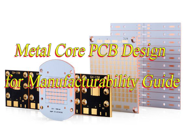
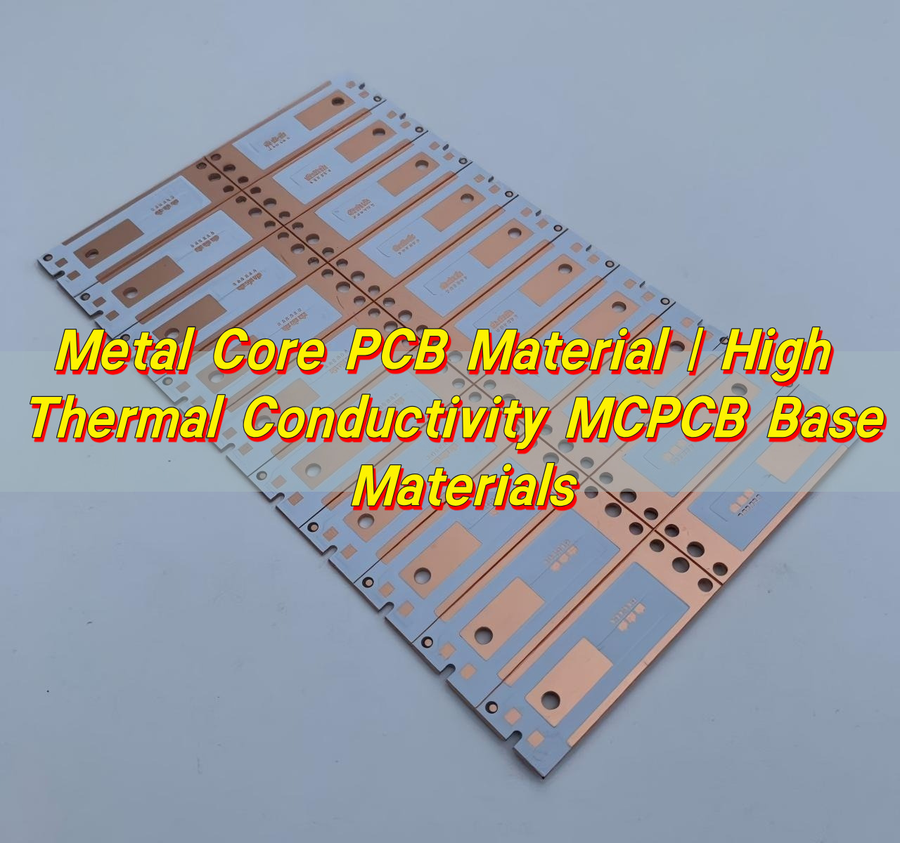
Electronic devices continue to shrink while power density keeps rising. Excess heat can shorten component life, reduce performance, and cause signal instability. Because of this, designers often select metal core PCB material instead of conventional laminates when thermal control becomes critical.
A metal core circuit board integrates a thermally conductive metal base beneath the dielectric and copper circuitry. This structure creates a direct path for heat to travel away from components. Compared with standard FR-4 boards, metal core PCBs can dissipate heat more efficiently and maintain better thermal balance during operation.
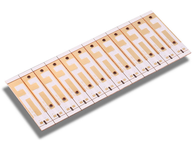
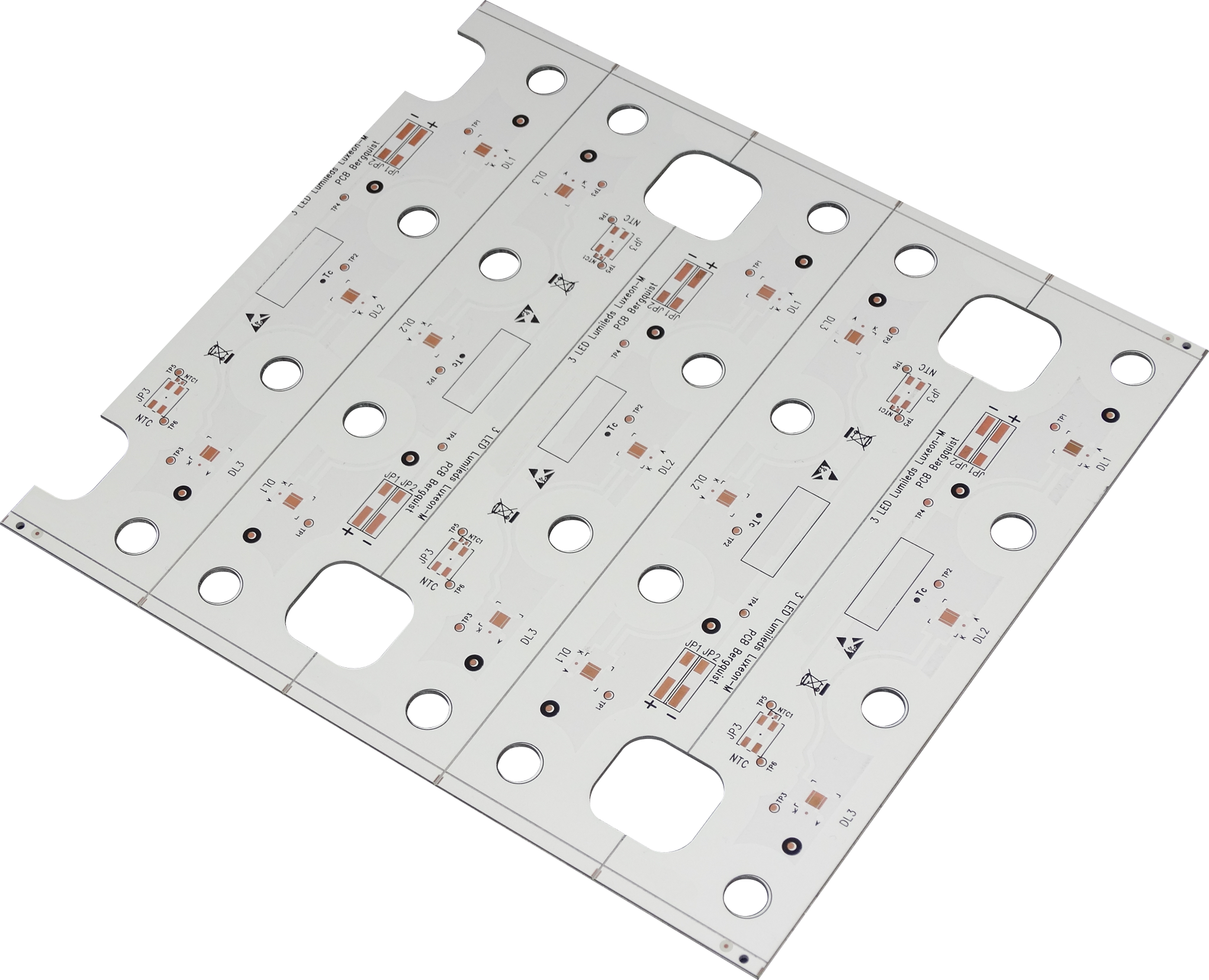
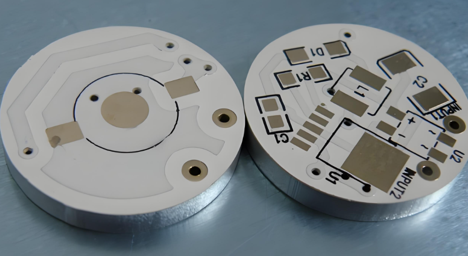
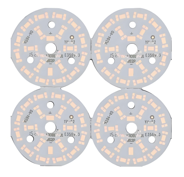
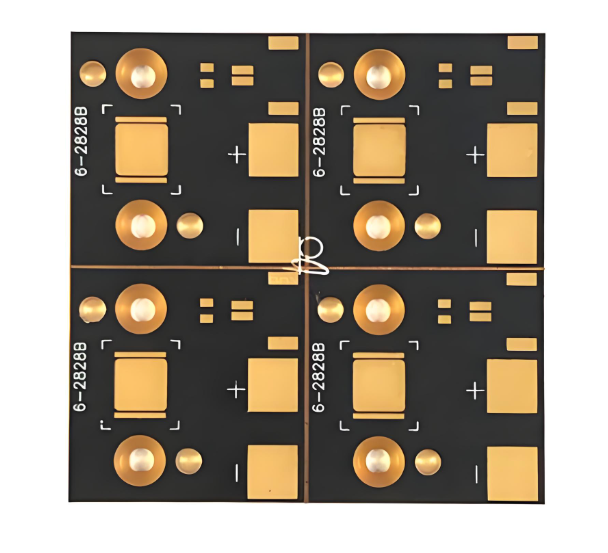
These boards are widely used in high-power LED lighting, automotive electronics, power converters, industrial control systems, and communication equipment. As power levels increase and device footprints shrink, engineers increasingly rely on aluminium core PCB, copper core PCB, and IMS PCB (Insulated Metal Substrate) technologies to stabilize thermal performance.
EBest Circuit (Best Technology)’s metal core PCB material provides excellent thermal conductivity, high stability and reliable performance for LED, power and high‑heat electronic applications.
What materials are used in metal core PCB?
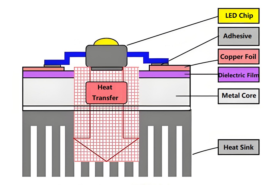
A typical metal core PCB material structure consists of three primary layers. These layers work together to transfer heat efficiently from components to the metal substrate. Each layer performs a specific thermal and electrical function that ensures stable circuit performance.
The typical MCPCB stack structure includes:
- Copper circuit layer
- Thermal dielectric layer
- Metal base layer
1. Copper Circuit Layer
The top layer contains copper traces that form the electrical circuit. This layer functions similarly to the copper layer in standard PCBs. Thicker copper improves current carrying capability and also spreads heat across the board surface. Copper thickness usually ranges from:
| Copper Thickness | Typical Use |
|---|---|
| 1 oz (35 μm) | Standard LED and low-power circuits |
| 2 oz (70 μm) | Power LED modules |
| 3 oz – 4 oz | High-current power electronics |
2. Thermal Dielectric Layer
The dielectric layer is a critical part of metal core PCB material. It electrically isolates the circuit from the metal base while still allowing heat to pass through. High thermal conductivity dielectric materials allow heat to move quickly from components into the metal base. Typical dielectric properties include:
| Property | Typical Range |
|---|---|
| Thermal conductivity | 1 W/mK – 10 W/mK |
| Thickness | 50 μm – 150 μm |
| Breakdown voltage | 2 kV – 6 kV |
Common dielectric fillers include:
- Ceramic particles
- Aluminum oxide
- Silicon compounds
These fillers increase thermal conductivity while maintaining insulation strength.
3. Metal Base Layer
The bottom layer of a pcb metal core acts as the primary heat sink. It spreads heat over a large surface area and transfers it to the external environment. Aluminum is widely used because it provides strong thermal performance at a reasonable cost. Copper offers the highest thermal conductivity but is heavier and more expensive. The most common base materials are:
| Metal Base Type | Thermal Conductivity |
|---|---|
| Aluminum | ~200 W/mK |
| Copper | ~385 W/mK |
| Steel | ~50 W/mK |
How to choose metal core PCB material?
Selecting the right metal core pcb material depends on several engineering factors. The design must balance thermal performance, mechanical strength, electrical insulation, and manufacturing cost.
1. Thermal conductivity requirement
Heat dissipation is the main reason for using IMS PCB technology. The thermal conductivity of the dielectric layer determines how quickly heat moves into the metal base. Higher conductivity improves cooling performance. Typical ranges include:
| Thermal Conductivity | Application |
|---|---|
| 1–2 W/mK | Standard LED lighting |
| 3–5 W/mK | Automotive lighting |
| 5–10 W/mK | High-power electronics |
2. Electrical insulation performance
Although the metal base conducts heat well, it must remain electrically isolated from the circuit layer. Reliable insulation prevents short circuits and protects sensitive components. Designers must verify:
- Dielectric breakdown voltage
- Insulation resistance
- Long-term reliability under temperature cycling
3. Mechanical stability
Mechanical strength is also important when selecting metal core PCB materials. Aluminum substrates provide good rigidity while keeping board weight low. Copper base boards offer superior strength but increase overall board mass.
4. Manufacturing compatibility
Manufacturers evaluate whether the material supports standard processes such as:
- SMT assembly
- reflow soldering
- drilling and routing
- surface finishing
A stable material simplifies production and improves yield.
What material is the MCPCB made of?
An MCPCB (Metal Core Printed Circuit Board) typically combines three major materials: copper circuitry, thermal dielectric, and a metal substrate. However, within this structure, several variants exist depending on the application.
Aluminum Core PCB
An aluminium core PCB is the most widely used type of MCPCB. Aluminum offers excellent thermal conductivity while remaining lightweight and cost-effective. Typical aluminum grades used include:
- 5052 aluminum
- 6061 aluminum
- 1060 aluminum
Advantages of aluminum core PCB include:
- Lightweight structure
- Good heat dissipation
- Low material cost
- Stable mechanical properties
Because of these benefits, aluminum core boards dominate LED lighting and power modules.
Copper Core PCB
A copper core PCB uses a solid copper substrate instead of aluminum. Copper has almost double the thermal conductivity of aluminum. This allows heat to move even faster away from components. However, copper boards are heavier and more expensive. Copper core PCBs are often used in:
- high-power LEDs
- RF power amplifiers
- motor drivers
- automotive electronics
IMS PCB (Insulated Metal Substrate)
An IMS PCB refers to a board where a dielectric layer isolates the circuit from the metal base. Most metal core PCBs fall into this category. The IMS structure allows designers to combine electrical insulation with thermal efficiency.
Typical IMS stack: Copper layer → thermal dielectric → aluminum base. This structure provides excellent heat dissipation while maintaining electrical isolation.
How thick is the metal core PCB?
The metal core pcb thickness varies depending on the design requirements. Engineers must consider both electrical performance and heat transfer efficiency. A typical MCPCB includes several thickness parameters.
Total board thickness. Thicker boards often improve mechanical strength. Common board thickness values include:
| Board Thickness | Application |
|---|---|
| 1.0 mm | Thin LED modules |
| 1.6 mm | Standard MCPCB |
| 2.0 mm | High-power lighting |
| 3.2 mm | Power electronics |
Metal core thickness. The metal base itself can vary significantly. A thicker metal base improves heat spreading capacity.
| Metal Core Thickness | Typical Range |
|---|---|
| Aluminum base | 0.8 mm – 3.0 mm |
| Copper base | 1.0 mm – 4.0 mm |
Dielectric thickness. The dielectric layer usually ranges between: 50 μm – 150 μm. A thinner dielectric improves thermal transfer but must still provide reliable electrical insulation.
Why is thermal conductivity important in metal core PCB material?
Thermal conductivity determines how quickly heat moves through a material. In electronic circuits, efficient heat removal protects components and stabilizes performance. High temperatures can reduce LED brightness, affect semiconductor switching speed, and shorten component lifespan.
A well-designed metal core PCB material structure solves this problem by creating a direct thermal path. Because the metal base spreads heat efficiently, the board avoids localized hot spots.
Heat flows through the following stages:
- Component generates heat
- Heat enters copper circuit layer
- Heat moves through dielectric layer
- Heat spreads across metal substrate
- Heat dissipates into air or heat sink
Typical thermal conductivity comparison:
| Material | Thermal Conductivity |
|---|---|
| FR-4 | 0.3 W/mK |
| Aluminum base | ~200 W/mK |
| Copper base | ~385 W/mK |
What are benefits of metal core PCB material?
The advantages of metal core pcb materials extend beyond thermal performance. Engineers often select them because they improve reliability and design flexibility. Several benefits stand out. These advantages make pcb metal core technology suitable for high-power electronics.
- 1. Excellent heat dissipation
Metal substrates rapidly transfer heat away from components. This reduces thermal stress and improves long-term reliability.
- 2. Improved circuit stability
Stable temperatures keep semiconductor devices operating within their optimal range.
- 3. High mechanical strength
Metal substrates increase board rigidity and durability.
- 4. Compact product design
Efficient heat transfer allows designers to place components closer together.
- 5. Longer product lifespan
Lower operating temperature helps protect LEDs, ICs, and power components.
- 6. Reduced external cooling requirements
Many MCPCB designs operate without large heat sinks.
What is the difference between metal core PCB and FR4?
A metal core PCB vs FR4 comparison highlights the fundamental differences between the two technologies.
FR-4 is a fiberglass epoxy laminate commonly used in conventional PCBs. While it offers good electrical insulation, it has limited thermal conductivity. Metal core boards replace the fiberglass base with a thermally conductive metal substrate. In applications with high power density, metal core circuit boards offer clear advantages.
Below is a comparison of the two materials.
| Feature | Metal Core PCB | FR-4 PCB |
|---|---|---|
| Base material | Aluminum or copper | Glass fiber epoxy |
| Thermal conductivity | High | Low |
| Heat dissipation | Excellent | Limited |
| Mechanical strength | Strong | Moderate |
| Weight | Heavier | Lightweight |
| Typical applications | LEDs, power electronics | Consumer electronics |
Where is metal core PCB material used?
Because of its thermal advantages, metal core PCB material appears in many modern electronic systems. Industries rely on MCPCBs to manage heat in compact designs. Common applications include:
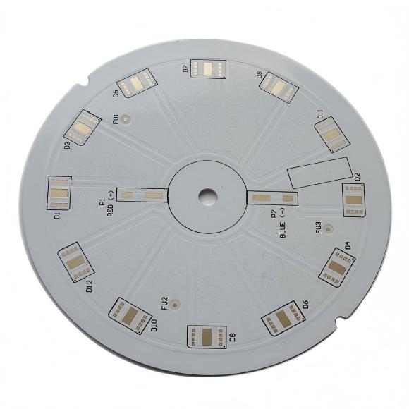
LED lighting, High-power LEDs generate substantial heat. MCPCBs help maintain consistent brightness and extend LED life.
Examples include:
- street lighting
- automotive headlights
- industrial lighting
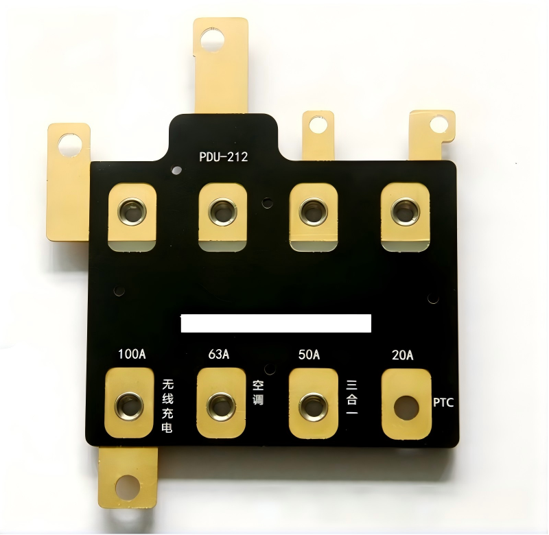
Automotive electronics, Vehicles require reliable thermal management for components such as:
- engine control modules
- power converters
- lighting systems
Power electronics, Power supplies and converters generate high heat density. Metal core boards stabilize thermal performance in:
- motor drives
- DC-DC converters
- industrial power modules
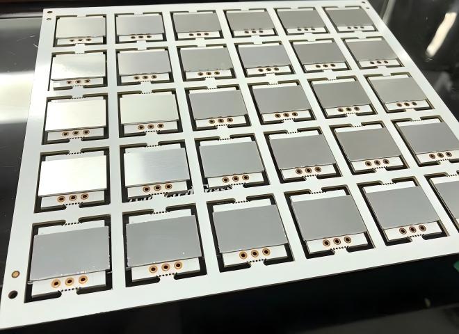
Communication systems, RF amplifiers and communication equipment often use copper core PCB structures to dissipate heat from power devices.
Consumer electronics, Compact devices such as projectors and audio equipment also benefit from MCPCB technology.
At EBest Circuit (Best Technology), we specialize in manufacturing high-quality metal core PCBs and thermal management circuit boards for demanding applications. Our engineering team supports customers from design review to production, ensuring each board meets strict performance standards.
If you are developing high-power electronic products and need reliable metal core PCB materials, feel free to contact our team. Email: sales@bestpcbs.com