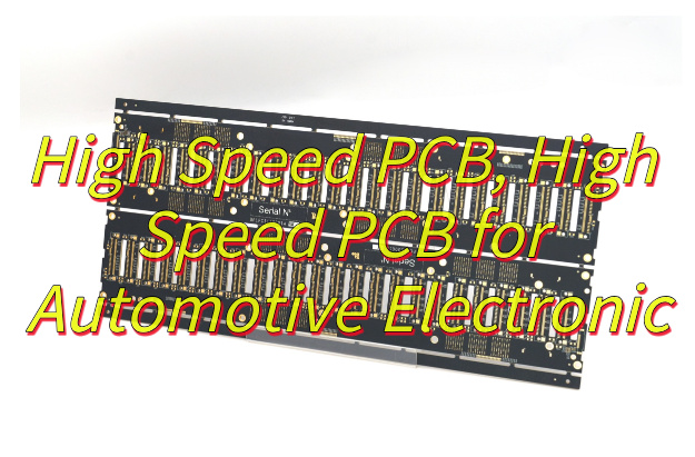
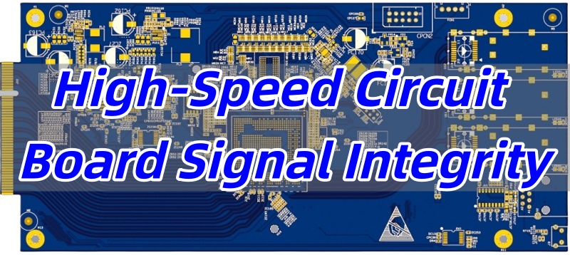
High-speed circuit board signal integrity is crucial for ensuring that modern electronic systems operate efficiently and reliably. The blog presents key strategies for enhancing signal integrity in high-speed circuit boards, covering fundamental aspects including PCB signal integrity, power integrity, rise time and bandwidth optimization, common design challenges, the critical role of interconnect design, effective design principles, and essential evaluation methods.
Have you encountered these operational challenges?
- Signal reflection/distortion caused by impedance mismatch?
- Crosstalk/noise-induced bit errors?
- Signal attenuation from dielectric loss/material inconsistency?
- Via/trace design issues degrading signal quality?
- Impedance drift due to temperature fluctuations?
EBest Circuit (Best Technology) tackles these obstacles with the following workable solutions.
- Impedance Control Technology
- Implement impedance-controlled layers during design
- Precise control of substrate thickness/trace width
- Ensures trace impedance matches characteristic impedance
- Significantly reduces signal reflection
- Low-Loss & Consistent Materials
- High-frequency substrates like Rogers 4350/5880 with stable Dk
- Strict batch parameter verification
- Minimizes dielectric loss and Dk mismatch
- Trace Layout & Differential Pair Optimization
- Optimal signal routing topology
- Sufficient spacing between high-speed/sensitive signals
- Equal-length differential pairs with termination resistors
- Suppresses crosstalk/common-mode noise
- Precision Via Processing
- Back-drilling/micro-vias for critical high-speed paths
- Via fencing and blind/buried hole techniques
- Reduces parasitic inductance/impedance discontinuities
- Full-Process Temperature Compensation
- Real-time monitoring of temperature/thickness/alignment
- Temperature-impedance compensation testing
- Material compatibility validation
- Ensures impedance stability across temperature ranges
In 5G, AI-IoT, and autonomous driving applications, signal integrity has emerged as the critical factor determining system reliability. EBest Circuit (Best Technology) addresses this challenge through advanced manufacturing and testing equipment, high-precision material selection, and a dedicated high-speed PCB design team, achieving over 30% improvement in signal integrity performance. With nearly 20 years of specialized experience in high-speed PCB manufacturing, we provide comprehensive solutions covering prototype development, high-volume production, and fully assembled boards. Our production processes strictly comply with ISO 9001, ISO 13485, IATF 16949, AS9100D, UL certification, and REACH, RoHS standards. For high-speed PCB requirements, contact our sales team at sales@bestpcbs.com for customized solutions tailored to your application needs.
What is signal integrity in PCB?
Signal Integrity (SI) refers to the ability of a signal to maintain its original electrical characteristics—such as waveform, timing, and amplitude—without distortion during transmission across a PCB. It examines the interaction between the electrical properties of interconnects (like traces and transmission lines) and the signal waveform to ensure high-quality signal delivery from the transmitter to the receiver.
Manifestations of SI Problems
- Timing Issues: Signal delay or clock skew causing timing violations.
- Waveform Distortion: Ringing, reflections, and non-monotonic behavior.
- Noise and Interference: Crosstalk, ground bounce, power noise, and electromagnetic interference (EMI).
- Other Issues: Switching noise, signal attenuation due to capacitive loads, and electromagnetic radiation.
Root Causes
Short rise times are a primary contributor. Even with an unchanged circuit topology, the use of ICs with very fast rise times can cause previously stable designs to fail. High-speed signals are more sensitive to the electrical characteristics of interconnects, including impedance and parasitic elements.
Impact and Importance
Poor signal integrity can lead to data errors, timing violations, reduced system performance, or even complete system failure. It is a critical challenge in high-speed PCB design and directly affects system reliability, power consumption, and electromagnetic compatibility (EMC).
Design Relevance
SI issues highlight that interconnects are not ideal conductors—their impedance, propagation delay, and parasitic capacitance/inductance interact with signals. Optimizing SI requires controlled impedance matching, termination strategies, layout rules, and stack-up design.
In summary, signal integrity in PCBs ensures that high-speed signals maintain waveform quality during transmission, preventing distortion caused by interconnect characteristics and ensuring stable system operation.
What is power integrity?
Power Integrity (PI) is the engineering discipline focused on ensuring a stable, clean, and adequate supply of current to all active devices on a board, enabling them to reliably switch between logic states (0s and 1s). Its primary goal is to minimize voltage fluctuations on the Power Delivery Network (PDN)—comprising voltage regulators, board planes, traces, decoupling capacitors, and vias—especially at the power pins of an integrated circuit (IC).
The fundamental distinction from Signal Integrity (SI) is one of focus:
- SI concerns the signal. It analyzes the quality, timing, and fidelity of the voltage waveform as it travels from a transmitter to a receiver on a dedicated path. The goal is to ensure a received ‘1’ looks like a ‘1’.
- PI concerns the energy. It analyzes the distribution network that supplies the current needed to create those signals. The goal is to ensure the voltage remains stable when the IC demands a sudden, large switching current.
Their relationship is symbiotic and inseparable:
- PI is the foundation for SI. A poor power supply (high PDN impedance) will manifest as signal-quality issues like jitter and noise.
- Conversely, signal switching activity (an SI concern) is the primary source of power noise (a PI problem), such as Simultaneous Switching Noise (SSN).
They converge physically at structures like vias, where the PDN acts as the return current path for signals.
In essence, Signal Integrity is about communication quality, while Power Integrity is about energy supply. You cannot have robust and reliable signal transmission without a first-class power delivery system.
How do rise time and bandwidth affect high-speed PCB design signal integrity?
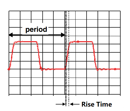
Rise time refers to the interval during which a signal transitions from 10% to 90% of its final value. In most high-speed systems, the allocated rise time is typically about 10% of the clock period (this is an empirical rule; for some FPGAs, it may be as short as 1% of the clock period).
Based on the above rule of thumb:
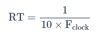
RT = Rise Time (in ns);
Fclock = Clock Frequency (in GHz)
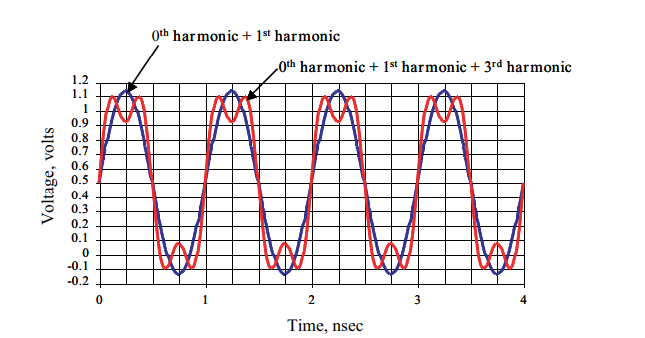
Bandwidth refers to the highest significant sinusoidal frequency component in a signal’s spectrum (note that the definition of bandwidth can vary across different fields). For example, using the 0th, 1st, and 3rd harmonics to construct a time-domain waveform, the highest significant sinusoidal component is 3 GHz, so the bandwidth is 3 GHz.
The empirical relationship between bandwidth and rise time (this estimate is generally slightly lower than the actual requirement; if the design meets this estimate, the actual requirement will also be satisfied) is: BW = 0.35 / RT
Where:
- BW = Bandwidth (GHz)
- RT = Rise time from 10% to 90% of the signal (ns)
Interconnect bandwidth refers to the highest sinusoidal frequency component that can be transmitted through the interconnect without significant loss (note the distinction from the signal bandwidth mentioned earlier, which refers to the signal itself; interconnect bandwidth refers to the PCB’s transmission capability). It is generally defined as the frequency at which the signal amplitude drops to 70% of the input amplitude, also known as the 3 dB bandwidth. In practice, when a signal propagates through the interconnect, its rise time will typically degrade.
Pls kindly note that rise time and bandwidth directly influence signal integrity in high-speed PCB designs. Faster rise times introduce higher frequency components, which interact more strongly with PCB traces, vias, and connectors. If these elements are not properly designed, the signal may experience reflections, ringing, overshoot, and crosstalk, leading to waveform distortion and timing errors.
Limited bandwidth in PCB interconnects can further degrade the signal’s high-frequency components, slowing down rise times and reducing the fidelity of waveform transmission. To preserve signal integrity, the PCB layout must ensure sufficient bandwidth, controlled impedance, and proper trace spacing. Effective management of rise time and bandwidth helps maintain clean transitions, minimize noise coupling, and ensure reliable high-speed data transfer.
What are the common types of signal integrity problems in high-speed boards?
High-speed boards often encounter six main SI issues:
- Single-network distortion: Signals within a single trace can deform due to impedance mismatch or dielectric inconsistencies.
- Frequency-dependent losses: High-frequency components degrade over long interconnects, slowing rise times.
- Crosstalk: Interference between neighboring traces can corrupt data signals.
- Ground and power bounce: Switching currents cause transient voltage variations that propagate to signals.
- Plane collapse: Weak power/ground planes can cause voltage dips affecting overall SI.
- Electromagnetic interference (EMI): External or internal sources induce unwanted signals in sensitive traces.
Recognizing these problems early allows designers to implement targeted solutions before production, reducing costly revisions.
How does interconnect design influence high-speed digital PCB signal integrity?
Interconnect design is critical for maintaining clean signals. Factors include:
- Trace impedance: Keeping consistent impedance reduces reflections and waveform distortions.
- Trace length matching: Equalizing path lengths prevents timing mismatches and skew in differential signals.
- Layer stacking: Proper placement of ground and power planes shields signals from noise.
- Trace routing: Avoiding 90° bends, reducing stubs, and maintaining clearance reduces crosstalk and EMI.
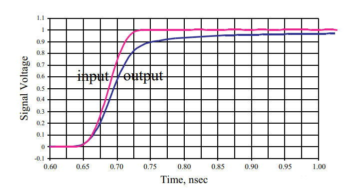
For example, a 4-inch 50Ω FR4 trace may show rise time degradation from 50ps to 67ps at the output, highlighting the importance of careful interconnect design for high-speed circuits.
What design principles can improve high-speed PCB signal integrity?
Improving signal integrity (SI) in high-speed digital PCBs requires a structured approach that integrates interconnect optimization, power distribution design, and electromagnetic compatibility control. Effective strategies span from layout planning and material selection to verification and failure analysis.
1. Interconnect and Transmission Path Optimization
Signal routing is the foundation of SI. Differential pairs must maintain strict symmetry, with spacing typically kept within twice the line width to avoid common-mode noise. Stripline structures generally outperform microstrips, as the dual reference planes provide a more stable impedance environment. Minimizing via usage is critical, since each via contributes approximately 0.5–1.0 nH of parasitic inductance, which at 10 GHz equates to 31–63 Ω of reactance. Back-drilling unused via stubs can reduce reflection coefficients by more than 40%. Length matching in high-speed buses, especially DDR or SerDes channels, must remain within ±5 ps to avoid skew-related timing failures.
2. Power Delivery Network (PDN) Design
Stable power is the prerequisite for clean signals. Decoupling capacitors should follow the “1–10–100” rule: place 0.1 µF ceramic capacitors within 1 mm of IC power pins, 10 µF tantalum capacitors within 10 mm, and 100 µF electrolytic capacitors within 100 mm. Local mounting inductance should be below 0.5 nH; using 0402 packages instead of 0603 reduces parasitics by ~30%. The 20H rule should guide power–ground spacing, where the edge clearance between planes is at least 20× the dielectric thickness, effectively suppressing fringing radiation.
3. Impedance Control and Signal Matching
Accurate impedance control prevents reflections and ringing. For microstrip lines, impedance can be estimated using:
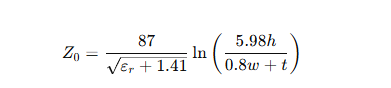
where h is dielectric thickness, w trace width, and t copper thickness. Differential impedance must account for coupling; when spacing S ≤ 3w, the coupling factor K ≥ 0.2, and the corrected formula becomes Zdiff = 2Z0 (1 – K). Test points should have pad diameters ≤0.4 mm and trace lengths ≤5 mm to minimize disturbance during impedance validation.
4. Electromagnetic Compatibility (EMC) Practices
Layer stacking and shielding are essential. Sensitive circuits should be routed in inner layers and enclosed between continuous ground planes. Critical clock traces should observe the 3W rule, where spacing is at least three times the trace width. Ground via fences placed at λ/10 spacing provide return paths and suppress EMI; at 10 GHz this corresponds to ~7.5 mm. Ferrite beads must be selected based on the noise spectrum, with DC resistance kept below 0.1 Ω and current ratings derated by 50%.
5. Thermal and Manufacturing Considerations
Signal quality is also tied to thermal stability. Copper trace current capacity follows IPC-2221 guidelines, where trace cross-section and temperature rise dictate maximum allowable current. Arrays of thermal vias should maintain a 3:1 aspect ratio with plating ≥25 µm. For high-power devices, component placement should align with airflow direction to improve cooling efficiency. Material choice is critical: FR4 (tanδ ≈ 0.02) is unsuitable beyond ~10 GHz, while Rogers RO4350B (tanδ ≈ 0.0037) supports operation above 28 GHz. Surface finishes such as ENIG (0.05–0.1 µm gold, 3–5 µm nickel) offer solder reliability for repeated thermal cycles.
6. Verification and Testing
SI must be validated in both time and frequency domains. Eye diagrams should maintain a vertical opening >200 mV and horizontal width >0.7 UI. S-parameter testing should confirm return loss S11 < –10 dB and insertion loss S21 variation within ±1 dB up to the third harmonic frequency. Near-field probes can measure PDN noise radiation, which should remain below 40 dBµV/m at 1 GHz. TDR (Time-Domain Reflectometry) with 5 ps resolution enables pinpointing impedance discontinuities to within 0.75 mm.
7. Adaptive and Advanced Methods
When board real estate is limited, embedded capacitance technology (<4 µm dielectric, 50 nF/cm²) can replace discrete decoupling capacitors. For ultra-high-speed SerDes (>56 Gbps), transmitter pre-emphasis (3–6 dB) and receiver equalization (CTLE + DFE) are mandatory to keep total jitter below 0.3 UI. In RF boards, cavity shielding and ground impedance <5 mΩ help isolate sensitive analog sections.
In summary, improving high-speed PCB signal integrity requires more than simple layout hygiene. It involves a holistic design methodology combining interconnect control, PDN optimization, EMC discipline, and rigorous validation. Applying these principles systematically enables robust, low-noise, and high-reliability digital systems capable of sustaining multi-gigabit signaling.
How can engineers evaluate and test high-speed circuit board signal integrity?
Ensuring high-speed circuit board signal integrity is critical for reliable PCB performance in high-speed digital systems. Engineers leverage a combination of theoretical analysis, simulation, and physical testing to detect and mitigate signal degradation, crosstalk, and reflection, ensuring that high-speed circuit designs meet rigorous performance standards.
1. Layout and Routing Rules for Signal Integrity
Proper PCB layout is the foundation for high-speed signal integrity. Engineers implement controlled impedance traces, maintain adequate spacing between signal lines, avoid crossings, and use multi-layer routing to reduce crosstalk and signal coupling. These design principles improve waveform fidelity and reduce the likelihood of SI issues when tested on real circuits.
2. Transmission Line Analysis for High-Speed Signals
Transmission line theory models signal propagation along PCB traces and interconnects. Engineers use these models to predict waveform behavior, propagation delays, and amplitude changes, preventing reflections, ringing, and overshoot. Transmission line modeling is essential for understanding high-speed signal behavior and is widely used in high-speed signal integrity analysis.
3. Electromagnetic Simulation
Electromagnetic simulation allows engineers to model the PCB’s electric and magnetic fields, analyzing signal paths, trace coupling, and potential interference. Tools such as HFSS and ADS help predict issues in signal integrity in PCB designs and evaluate how layout changes affect both signal and power integrity. EM simulation enables optimization before fabrication, reducing costly post-production fixes.
4. Time-Domain Analysis
Time-domain methods observe real signal waveforms over time. High-speed oscilloscopes and logic analyzers capture waveform quality, rise and fall times, and signal transitions. Engineers detect distortion, reflections, overshoot, and ringing. Time-domain analysis is a key step in both high-speed circuit board signal integrity testing and design verification.
5. Frequency-Domain Analysis
Frequency-domain analysis examines the spectral content of signals to identify bandwidth limitations, resonances, or uneven frequency responses. Using spectrum analyzers and network analyzers, engineers evaluate high-frequency behavior, EMI interactions, and crosstalk. This method is particularly useful for ensuring high-speed signal integrity simulation accurately reflects real-world operating conditions.
6. Timing Analysis and Clock Integrity
Timing analysis focuses on clock-related relationships and signal stability. Engineers use timing analyzers or clock extraction software to detect clock skew, jitter, and synchronization errors. Accurate timing analysis ensures reliable high-speed data transfer, supporting circuit integrity cables and overall system performance.
7. Comprehensive Signal Integrity Validation Workflow
A complete workflow combines multiple stages to verify high-speed PCB signal integrity:
- Design Rule Check (DRC): Ensures layout compliance and identifies potential SI issues.
- Electromagnetic Simulation: Predicts signal propagation and interconnect coupling effects before fabrication.
- Time-Domain Measurement: Observes waveform quality, rise/fall times, and detects reflection or overshoot.
- Frequency-Domain Measurement: Assesses bandwidth, resonance, and high-frequency signal loss.
- Timing Analysis: Confirms clock alignment and signal stability, ensuring synchronized high-speed operation.
Combining these methods provides a comprehensive approach to high-speed circuit board signal integrity testing, reduces costly design revisions, and guarantees stable performance in demanding high-speed digital applications.
Why choosing a reliable high-speed PCB supplier is essential for signal integrity?
Even the most meticulously designed high-speed PCBs can fail to achieve optimal signal integrity if the manufacturing process is inconsistent or poorly controlled. In high-frequency digital systems—especially those operating at multi-gigabit per second rates—minute variations in materials or fabrication can significantly degrade performance.
1. Material consistency and dielectric properties
High-speed signals are extremely sensitive to dielectric loss (Df) and dielectric constant (Dk) variation. Standard FR-4, with Df ≈ 0.02, may suffice for low-GHz applications but becomes unsuitable for digital circuits operating at 10 Gb/s or above, where higher harmonics carry critical high-frequency energy. Advanced PCB substrates, such as Rogers RO4003/4350B, Panasonic Megtron, Isola FR408HR, or TUC Tuc862/Tuc872SLK, offer ultra-low Df (down to 0.0015) and tightly controlled Dk, minimizing frequency-dependent signal attenuation. A reliable supplier ensures that these materials meet specifications consistently across the entire production batch, safeguarding the design’s intended high-speed performance.
2. Precision fabrication and layer alignment
High-speed designs demand precise control over copper thickness, trace width, and interlayer registration. Minor deviations can alter characteristic impedance, causing reflections, ringing, and crosstalk. For example, a slight variation in copper weight along a 50 Ω microstrip can increase insertion loss at high frequencies. Trusted suppliers employ rigorous process controls, including automated inspection and process monitoring, to guarantee accurate layer alignment and copper deposition.
3. Managing transmission loss and conductor effects
Transmission loss at high frequencies arises from dielectric absorption, conductor loss, and radiation. Conductor loss is frequency-dependent due to the skin effect, which forces current to the conductor surface at GHz frequencies, increasing effective resistance. Reliable manufacturers optimize trace surface finish, copper plating, and etching processes to minimize conductor loss and maintain uniform current distribution. This is essential for maintaining signal integrity in long traces or critical SerDes channels.
4. Thermal stability and reproducibility
High-speed circuits often operate under significant thermal load, and temperature-induced variations in material properties can impact impedance and timing. Quality PCB suppliers maintain tight control over material Tg (glass transition temperature), resin content, and lamination pressure, ensuring that the final board exhibits minimal warpage or thickness variation, even under thermal cycling.
5. Scaling from prototype to production
Maintaining signal integrity is not only critical during prototyping but across volume production. A reliable supplier provides consistent material batches, controlled processes, and reproducible trace parameters, reducing variation between prototypes and final products. This ensures that performance observed during design verification translates accurately to large-scale manufacturing.
6. Compliance and testing capabilities
High-end suppliers often integrate in-line testing, impedance verification, and high-frequency S-parameter validation to detect anomalies before boards leave production. These measures help identify deviations in Df, Dk, or copper thickness that could compromise SI, providing engineers with confidence that the manufactured boards will meet stringent high-speed requirements.
In a nutshell, choosing a reliable high-speed PCB supplier is essential because even minor material or fabrication inconsistencies can undermine signal integrity. Suppliers who provide tightly controlled substrate materials, precise layer alignment, optimized conductor processing, and thorough testing ensure that your high-speed designs perform as intended, from initial prototype to full-scale production. For critical digital systems—especially those operating at 10 Gb/s and beyond—partnering with a capable and experienced supplier is not just a convenience; it is a requirement for maintaining robust, low-loss, and reliable high-speed signal transmission.
How EBest Circuit (Best Technology) ensures superior high-speed PCB signal integrity?
EBest Circuit (Best Technology) addresses common customer pain points such as unexpected signal loss, EMI issues, and unreliable timelines. Our solutions include:
- ISO 9001, IATF 16949, and AS9100D certified manufacturing for precise tolerances.
- Advanced MES systems that track each component for full traceability.
- Professional engineering teams providing high-speed signal integrity simulations and layout guidance.
- Customized high-speed PCB designs to match specific performance requirements.
- Comprehensive supply chain, selecting suitable material according to your projects, such as Rogers RO4003、RO3003、RO4350、RO5880, Tuc862、872SLK、883、933, etc.
By combining rigorous quality control with engineering expertise, we ensure your high-speed PCB meets signal integrity standards while reducing risks and improving product reliability.
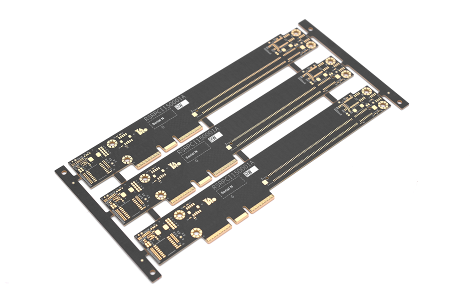
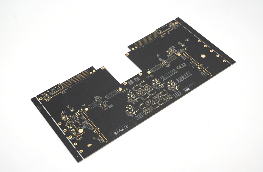
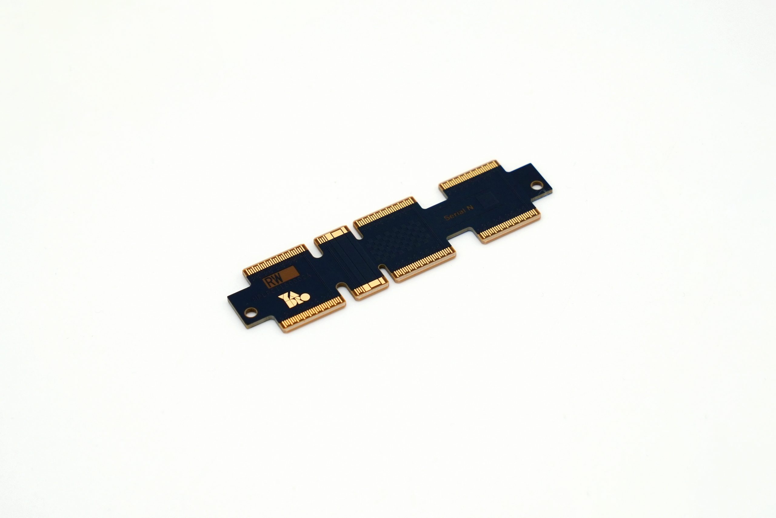
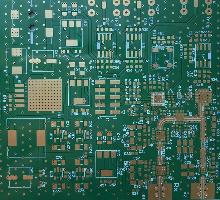
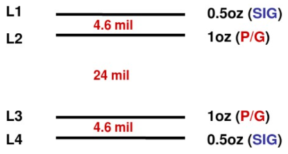
Case of high-speed circuit board signal integrity in EBest Circuit (Best Technology)
4-Layer Board
Template A:
■ Material: FR4
■ Impedance Type: Standard Characteristic Impedance
■ Board Thickness: 2.0mm ±0.2mm
■ Impedance Design Line Width: 9mil
■ Finished Impedance: 50Ω ±5Ω
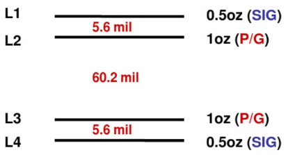
Template B:
■ Material: FR4
■ Impedance Type: Standard Characteristic Impedance
■ Board Thickness: 1.0mm ±0.2mm
■ Impedance Design Line Width: 6.5mil
■ Finished Impedance: 50Ω ±5Ω
In closing, high-speed circuit board signal integrity is vital for modern electronic systems. Understanding high-speed circuit board signal integrity, power integrity, rise time, bandwidth, interconnect design, technical design principles, and testing methods allows engineers to prevent distortions and timing errors.
EBest Circuit (Best Technology) provides a one-stop solution for your high-speed PCB signal-integrity challenges. We employ low-Dk, low-Df high-frequency substrate materials and tightly couple internal routing with reference planes to minimize crosstalk and EMI. You will benefit from our end-to-end service: requirement assessment → design simulation → prototype validation → volume production, with a dedicated project manager overseeing the entire process to ensure a 20% reduction in delivery time. By performing a single, comprehensive SI optimization, we eliminate rework and scrap, saving customers between 15% and 25% of manufacturing costs. Should you have a high-speed PCB project that demands superior signal integrity, please contact our sales team at sales@bestpcbs.com.