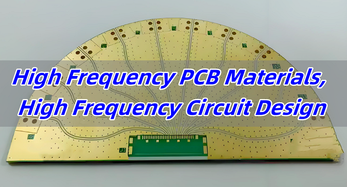
Have you ever wondered why engineers talk about high frequency PCB and high speed PCBs as if they’re completely different technologies—even though they both deal with signals in the GHz range? It’s a common point of confusion, and the truth is that these two types of circuit boards serve very different purposes, even if they sometimes overlap in the same system.
Whether you’re designing RF modules, 5G antennas, or high-speed digital hardware, this article gives you the clarity you need to make the right technical decisions.
What Is a High Frequency PCB?
A high frequency PCB is a printed circuit board designed to operate at frequencies above 500 MHz, and in RF/microwave applications typically from 1 GHz to 77 GHz (and beyond). These circuits carry analog RF signals where signal integrity depends heavily on dielectric behavior, phase stability, and transmission line accuracy.
Because electromagnetic waves at these frequencies are extremely sensitive to loss, materials and PCB structures must remain consistent across the entire board.
Key characteristics of high frequency PCBs include:
Very low dielectric loss (Df ≤ 0.005 in many RF materials)
Stable dielectric constant (Dk tolerance within ±0.03)
High dimensional and thermal stability
Precise impedance-controlled transmission lines
Use of specialized laminates like Rogers, Taconic, or PTFE-based materials
High frequency PCBs are essential in RF, 5G millimeter wave, radar, satellite systems, and microwave communications.
What Is a High Speed PCB?
A high speed PCB focuses on the integrity of digital signals with fast rise/fall times (not necessarily high analog frequency). In high-speed digital design, the primary goal is to ensure that the signal transitions propagate without distortion, crosstalk, jitter, or timing failures.
High speed PCBs usually operate in the hundreds of MHz to several GHz, but the defining parameter is edge rate, not the signal frequency.
Key characteristics of high-speed PCBs:
Strong emphasis on impedance control for DDR, USB, PCIe, HDMI, and SerDes
Controlled routing for skew, timing, return path, and crosstalk
Use of PCB materials with low loss (Df 0.008–0.02) for digital integrity
Multilayer stackups optimized for reference planes, differential pairs, and power integrity
High-speed PCBs are used in servers, automotive ADAS, AI hardware, IoT devices, consumer electronics, and cloud networking systems.
High Frequency PCB vs High Speed PCB: What Are the Key Differences?
Both board types deal with fast signals, yet they solve different engineering problems. A high frequency PCB focuses on electromagnetic behavior in continuous-wave or modulated analog systems. A high speed PCB focuses on digital edges and their timing.
Both require impedance control, but HF PCBs rely heavily on material performance, while HS PCBs depend on layout and timing engineering.
What is Best Material for High Frequency PCB Design?
Material selection is very important in a PCB manufacturing. A good laminate must hold a stable dielectric constant and maintain low loss across temperature, humidity, and frequency. These attributes reduce insertion loss and stabilize impedance.
Widely used for 24 GHz and 77 GHz radar, antennas, and precision RF paths
2. Rogers RO4350B laminate
A hydrocarbon ceramic material with stable electrical performance.
Dk ≈ 3.48
Very good loss performance for mid-GHz RF
Easier to fabricate compared with PTFE
3. PTFE-based laminates (RO5880, Taconic, etc.)
PTFE delivers ultra-low loss and excellent Dk stability.
Ideal for satellite work
Strong performance in microwave and millimeter-wave designs
4. Hybrid stackups
Some designs combine PTFE layers with FR4 or hydrocarbon layers to balance cost and RF stability. This approach reduces material expense while keeping critical layers low-loss.
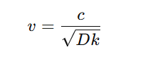
High frequency PCB materials must remain stable under frequency sweep. Even small Dk drift changes phase velocity and affects filter tuning, antenna gain, and RF link range. Material planning is one of the most important steps in high frequency PCB design.
High Frequency PCB Stackup and Impedance Control
High frequency stackups require precise control over dielectric thickness, copper profile, and trace geometry.
Key stackup considerations:
Dielectric thickness tolerance ±2–3%
Low-profile copper (VLP / RTF) to minimize conductor loss
Use of microstrip, stripline, and coplanar waveguides
Multiple ground layers for shielding
Tight impedance control (±5% or better)
Common impedance targets:
50Ω single-ended
75Ω for some RF systems
100Ω differential for high-speed digital + RF hybrids
High Frequency PCB Routing Rules for RF, 5G, and Microwave Designs
1. Use controlled-impedance transmission lines (microstrip/CPWG/stripline).
Wherever RF accuracy and low loss are critical, high frequency PCB materials dominate.
Why Choose EBest Circuit (Best Technology) as Your High Frequency PCB Supplier?
As a leading RF and microwave PCB manufacturer, EBest Circuit (Best Technology) provides stable production for demanding RF, 5G, and microwave applications. EBest Circuit (Best Technology) offers:
Over 17 years of RF PCB manufacturing experience
Support for Rogers, Taconic, PTFE, hydrocarbon, and hybrid stackups
High-precision impedance control ±5% or better
Ability to fabricate 1–40 layer HF multilayers
Low-profile copper and high-frequency plating capability
Advanced AOI, laser drilling, back-drill, and tight-tolerance machining
Full engineering DFM support for RF layouts
Proven reliability in defense, telecom, automotive radar, and aerospace projects
If you need RF or microwave PCB manufacturing with consistent performance, EBest Circuit (Best Technology) provides fast lead times, stable quality, and expert engineering support. Contact us get your PCB prototype right now!
FAQs
1. Is a high frequency PCB the same as an RF PCB?
Not exactly. RF PCBs are a subset of high frequency PCBs and usually refer to analog circuits under 6 GHz, while high frequency PCBs may go up to 100 GHz or more.
2. Can FR4 be used for high frequency PCB design?
FR4 can be used up to ~1 GHz, but losses become too large beyond that. Rogers or PTFE materials are recommended for low loss.
3. What is the typical impedance for RF PCBs?
50Ω single-ended and 100Ω differential are the most common.
4. What frequency is considered “high speed digital”?
Generally above 100 MHz clock, or any signal with rise times <1 ns.
5. Why is copper roughness important?
Rough copper increases conductor loss, especially above 10 GHz.
6. Can I combine FR4 and Rogers in the same PCB?
Yes, hybrid stackups reduce cost and are common in 5G and IoT RF modules.
7. What determines material selection for RF PCBs?
Loss tangent (Df), dielectric constant stability, thermal reliability, and manufacturing tolerance.
Not exactly. All RF PCBs fall under the high-frequency PCB category, but not all high-frequency PCBs qualify as RF PCBs.
RF PCB work sits at the center of many wireless systems, and an RF PCB often looks similar to a high frequency pcb. Many designers ask if they are the same board. They are related, yet each one handles different needs in signal flow, layout control, and material behavior.
As we move deeper into 5G, radar modules, and clean wireless designs, the differences become more visible. This article explains those differences in simple, clear language. More importantly, it guides engineers, buyers, and project teams on how to choose the right board for their next product.
What Is an RF PCB?
An RF PCB full name is Radio Frequency PCB, which is specifically handles signals in the radio frequency range: typically 300 MHz to 300 GHz, including microwave and millimeter-wave designs.
RF PCBs involve much stricter engineering constraints:
Tight impedance (<±5%) on microstrip, grounded CPW, stripline
Precise feature control (trace width tolerance around ±0.01–0.03 mm)
Stable dielectric properties across temperature
Very low-loss materials such as RO3003, RO4350B, RO5880, Taconic RF-35, PTFE woven/non-woven
Specialized stackups to avoid parasitic radiation
Careful via design to avoid stubs and resonance
Applications include:
Radar systems
Satellite communication
LNBs
RF front-end modules
Power amplifiers
Filters, couplers, antennas
RF PCB is wider use of 5G, IoT, and compact antennas has created strong demand for high-grade rf pcb builds. Because the signals travel along microstrip or CPW structures, the board behaves like part of the RF device, not only a carrier.
What Is a High-Frequency PCB?
A high-frequency PCB is any printed circuit board operating above roughly 500 MHz to 10 GHz+, depending on the design community.
Low dissipation factor (Df) for reduced signal loss
Good impedance control across long traces
Suitable materials like Rogers RO4003C, RO4350B, RO3003, PTFE, Isola I-Tera MT40, etc.
High-frequency PCBs serve applications such as:
5G modules
Wi-Fi devices
GPS receivers
High-speed digital layouts (DDR4/DDR5, SerDes)
High frequency boards focus on clean rise times, controlled impedance, and manageable dielectric loss. They support Wi-Fi, Bluetooth, high-speed digital lines, and mixed-signal designs. The design margin is wider than rf pcb work because the board deals with digital pulses, not pure RF energy.
High Frequency PCB
Key Differences Between RF PCB vs. High Frequency PCB
Aspect
High-Frequency PCB
RF PCB
Definition
Boards operating at high digital or analog frequencies
Boards designed specifically for RF signal transmission
The board contains microstrip, CPW, filters, or antennas
For example, a 2.4 GHz RF transceiver board using RO4350B is simultaneously:
a high-frequency PCB, because frequency is high
an RF PCB, because it processes RF signals
Thus, overlap exists, but they are not inherently identical.
Which One Should You Specify to Your PCB Supplier?
If your project handles RF transmission, always specify RF PCB so the manufacturer focuses on:
surface roughness control (Ra < 2 µm for low loss)
uniform dielectric thickness
controlled resin flow during lamination
tighter etching tolerance
Dk matching for microstrip/CPW accuracy
If it is only high-speed digital (e.g., PCIe, SerDes), then choose high-frequency PCB.
Why Do RF PCBs Need Special Materials Compared with High Frequency PCBs?
Material behavior influences both categories. Yet an rf pcb is more sensitive to the dielectric constant and copper profile.
RF units run energy through transmission lines. If the copper roughness increases loss, the system sees reduced range or gain shift. If the Dk drifts, the phase response moves. Because of this, the most common materials for rf pcb work include RO3003, RO4350B, RO5880, and PTFE blends.
In contrast, high frequency pcb materials can include Megtron series or Rogers 4000 series because the signal shape is less sensitive to phase stability. They still target low loss, but their working window is wider.
What Frequencies Define RF PCB Work vs High Frequency PCB Work?
Both ranges relate to how the signal behaves. RF work usually starts at 300 MHz and goes up to millimeter-wave. This includes radar, satellite, GPS, 24 GHz and 77 GHz systems, and many short-range radios.
High frequency ranges start from about 500 MHz to beyond 10 GHz. These support fast digital buses, Wi-Fi, and mixed-signal designs.
However, the frequency alone does not decide the board’s category. The final system function does.
Do RF PCBs Always Cost More Than High Frequency PCBs?
Actually yes when under the same design. RF boards use premium materials. These materials cost more because they hold stable Dk, low loss, and a smooth copper surface. They also require strict process control during drilling, plating, and lamination.
High frequency boards may use moderate-cost materials such as RO4003C or Megtron 4. They also need controlled lamination, yet the window for yield is wider.
Costs also rise when an rf pcb uses fine lines, tight impedance, or stacked microstrip structures. That said, skilled manufacturers can keep RF costs under control by optimizing stackup and process flow.
What Problems Occur When Designers Use the Wrong PCB Type?
If a design intended for RF is built on a standard high frequency pcb, several issues may appear:
Reduced communication range
Higher insertion loss
Unstable gain
Incorrect antenna tuning
Phase delay changes
EMC issues
Although not every situation is severe, these issues waste time in testing and rework.
When a high frequency digital board is produced using strict RF rules, the design remains stable. Yet the cost often rises without a visible performance gain.
What Tests Are Important for RF PCBs Compared with High Frequency PCBs?
RF boards often need tests beyond regular PCB checks. These include:
Dielectric thickness check
Dk variation review
Copper profile check
TDR impedance scan
S-parameter review after assembly
High frequency boards may also use TDR scans, yet the tolerance is wider. For RF, every shift affects the final device.
How Does EBest Circuit (Best Technology) Support RF PCB and High Frequency PCB Projects?
EBest Circuit (Best Technology) offers full material guidance, stackup review, transmission line advice, and strong quality assurance for both rf pcb and high frequency pcb builds. We handle small prototype lots and volume orders with the same care. Each rf pcb passes a detailed review, so the final product meets the performance target.
Our strengths include:
ISO9001, ISO13485, IATF16949, and AS9100D systems
Complete MES traceability
Tight impedance control
Fine etching for RF lines
Skilled process teams for PTFE and hybrid stackups
Smooth copper profile management
Fast prototype to mass build for global clients
We support antenna work, radar modules, filters, amplifiers, and mixed-signal boards. Our engineering team reviews each design before production to catch layout risks early to speed up product launches. For your next RF or high frequency project, our team stands ready to guide you from concept to delivery!
FAQs
1. Is an rf pcb the same as a high frequency pcb?
No. All RF boards are high frequency boards, but not all high frequency boards meet RF conditions.
2. Can I use RO4003C for both RF and high frequency PCB use?
Yes. However, many RF systems still need lower-loss materials such as RO3003 or RO5880.
3. Are RF boards harder to build?
Yes. They need tighter process control, smoother copper, and stable lamination.
4. How do I know if my design needs an rf pcb?
If your design uses antennas, filters, couplers, or PA modules, you need an RF board.
5. Does EBest Circuit (Best Technology) support RF and high frequency PCBA work?
Yes. We handle full assembly, tuning, connector installation, and testing.
High frequency laminate PCB board is the backbone of many modern communication, radar, and aerospace systems. This comprehensive guide covers points that include definition, material, features, layouts, costs, and applications of high-frequency PCBs. Besides, we have covered the insights about how to build a reliable PCB high frequency and where to get high frequency laminate PCB board.
Have you encountered these issues in your high frequency PCB communication circuits’ projects?
Greater design complexity and the relatively high requirement of designers?
Unstable operation due to the improper material selection or poor manufacturing process?
Full complexity of manufacturing, high requirements of equipment, and process control?
With these actionable solutions, even the toughest challenges can be overcome.
Optimize material selection: Balance performance and costs via selecting suitable materials of different application needs.
Boost design: Elevate layout and impedance control through innovative design tools and methods.
Adjust process control: Ensure the product performance and reliability by cutting-edge manufacturing process and strict quality control.
Get reliable cooperation and support: Get technical support and solution by collaborating with a professional high frequency PCB manufacturer and material suppliers.
As a high frequency PCB manufacturer, EBest Circuit (Best Technology) focuses on factory price PCB high frequency board prototyping, mass production, assembly with higher quality. Our product portfolio includes high frequency board PCB, high speed DAC board, high speed board, copper busbar PCB, HDI PCB, and others. We hold a competitive edge by improving product performance and effectively tackling customer pain points in high frequency PCB applications. We provide comprehensive technical support in material selection, design optimization, mass manufacturing, and quality control. If you have faced any PCB problems and want to get unique solutions for your projects, we would appreciate it if you could connect with us at sales@bestpcbs.com.
Generally, a circuit board with a frequency above 1 GHz can be considered a high frequency PCB.
With the advancement of technology, more designs are moving into:
The microwave range (>1 GHz)
The millimeter-wave range (>30 GHz)
Design Requirements High-frequency signals are extremely sensitive to the surrounding medium. Therefore, high frequency laminate PCB boards require:
Specialized laminate materials
Precise design and layout This ensures signal integrity, stability, and reliable performance.
Applications High frequency laminate PCB boards are widely used in advanced electronic systems where speed and low loss are critical, including:
High-frequency communication equipment
Radar and navigation systems
Automotive millimeter-wave radar
Satellite and aerospace electronics
In these fields, high-frequency PCB design is crucial to achieving reliable, stable, and efficient signal transmission.
Importance of Material The foundation of a high frequency PCB lies in its laminate material. Proper material selection directly determines how well the board performs in real applications. Key characteristics include:
Low dielectric constant (Dk): Maintains fast and stable signal transmission.
Low dissipation factor (Df): Reduces energy loss at high frequencies, improving transmission efficiency.
Excellent chemical stability: Ensures reliability in harsh conditions such as high temperature or humidity.
Additional Design Considerations Factors like PCB laminate thickness also influence impedance control and signal quality in high-frequency PCB design. Choosing the right high-frequency laminate PCB board material is therefore essential to achieving both reliability and performance in modern electronic devices.
Rigid PCB: High structural stability, suitable for precision circuits.
Flexible PCB: Bendable, ideal for space-constrained designs.
Rigid-Flex PCB: Combines rigidity and flexibility, perfect for complex layouts.
3. Structure Classification
Single-layer, double-layer, multi-layer boards.
High-frequency circuits typically use double-layer or multi-layer boards to ensure signal integrity and controlled impedance.
4. Common High-Frequency PCB Materials
PTFE (Polytetrafluoroethylene): Low signal loss, suitable for microwave frequency applications.
Ceramic-filled PTFE: Better heat dissipation and mechanical strength, suitable for high-power applications.
High-polymer Ceramic Materials: High thermal stability and stable dielectric constant, ideal for 5G and radar circuits.
RF Series High-Frequency Materials (e.g., ROGERS RO4000 series): Good processability, suitable for RF and microwave applications.
5. Leading Brands and Recommended Applications
Brand
Typical Models
Recommended Applications
ISOLA
Tachyon 100G
Antennas, RF modules
PANASONIC
R-5680 / R-5680N
High-frequency communication, microwave circuits
ROGERS
RO3003 / RO4350 / RO4730
Radar, 5G mainboards
TACONIC
RF35
High-speed signal transmission, RF boards
Shengyi
AW300
High-frequency communication boards, RF modules
6. Material Selection Tips
High-frequency signals or radar boards: Choose low-loss, thermally stable materials (ceramic-filled PTFE or ROGERS series).
Consumer electronics or general communication boards: Consider cost-effective organic materials with good processability.
High-power or high-heat applications: Opt for inorganic materials or thicker copper cores.
In summary, when selecting high-frequency PCB materials, it is essential to consider signal frequency, power, thermal management, and manufacturing complexity. By understanding the material properties and application requirements, engineers can choose the most suitable PCB material for optimal performance and reliability.
What is the Difference: High-Frequency PCB, High Speed PCB?
High-Frequency PCB
Definition: Designed to handle high-frequency signals, typically above 1 GHz.
Key Features: Signals are sensitive to materials and dielectric properties. Key factors include dielectric constant, loss factor, and thermal stability.
Design Focus:
Material selection: Low dielectric constant, low-loss materials such as PTFE, ROGERS, or ceramic-filled PTFE.
Impedance control: Critical for microwave and RF circuits.
Signal integrity: Minimizing signal attenuation and crosstalk.
Typical Applications: 5G communication modules, radar systems, antennas, RF equipment.
High-Speed PCB
Definition: Handles signals that change very quickly, focusing on fast rising and falling edges rather than just high frequency.
Key Features: Transmission line effects cannot be ignored due to rapid signal switching. Signal integrity, reflections, and crosstalk are the main design concerns.
Design Focus:
Trace length and routing: Careful layout to maintain signal integrity.
Impedance matching: Critical for high-speed data transfer.
Materials: Often improved FR4 or multi-layer boards, chosen to support high-speed digital signals.
Typical Applications: High-speed data buses, CPU interfaces, FPGA boards, high-speed memory interfaces.
High-Frequency PCB vs High-Speed PCB: Key Differences
Comparison Point
High-Frequency PCB
High-Speed PCB
Core Focus
Signal frequency (GHz and above)
Signal transition speed (fast rising/falling edges)
Material Requirements
Low dielectric constant, low loss
Signal integrity, impedance control
Common Materials
PTFE, ceramic, ROGERS series
Improved FR4, multi-layer boards
Typical Applications
Microwave, RF, radar, 5G
High-speed digital signals, CPU, FPGA, memory
Signal Characteristics
High-frequency, attenuation-sensitive
Fast-changing signals, reflection-sensitive
To conclude, high-frequency PCBs focus on handling high-frequency signals, where material choice is critical. While high-speed PCBs focus on fast signal transitions, emphasizing signal integrity and impedance control. In some cases, both aspects overlap—high-speed signals may also be high frequency, requiring attention to both material and design considerations.
What is High Frequency PCB Layout?
1. Keep RF Circuit Layout and Connections as Short as Possible
In high frequency circuits, impedance changes at transmission line corners can cause signal reflection. High-frequency signals may radiate as electromagnetic energy into the surrounding space. As a result, the signal level may drop after a “corner.”
Therefore, when designing high-frequency circuits, the RF layout must be carefully planned so that the corner angles of RF traces are minimized.
If there is enough space on the board, arrange RF components in as straight a line as possible. Straight-line placement and routing help prevent signal reflections and maintain signal levels to meet design requirements.
Key Point: In low-frequency circuits, right-angle traces can work normally. However, in high-frequency circuits, even minor variations in trace width affect the characteristic impedance, causing reflections and reducing signal levels.
2. Use Components or Rounded Corners at RF Trace Bends to Minimize Impedance Discontinuity
Following the principle of avoiding impedance discontinuities, if space allows, prioritize short and straight RF trace routing. If corners are unavoidable, avoid 90° or 45° angles. Use rounded traces instead. If a right-angle turn is necessary, place components strategically to create the turn through component positioning. This approach minimizes signal reflection caused by impedance changes.
Key Point: In high-frequency circuits, improving RF trace layout is crucial. Always follow the principle of avoiding characteristic impedance discontinuities.
3. Provide Separate Ground for Each Pad; Avoid Sharing Ground Vias
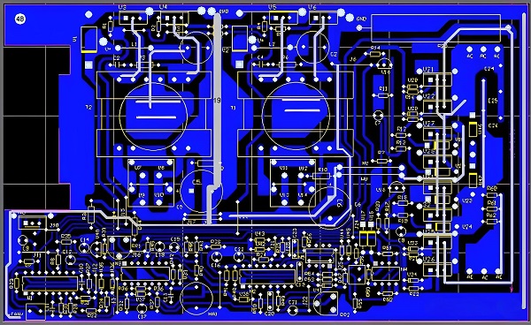
High-frequency PCB design requires careful management of RF trace-to-GND connections. In the picture above showing the incorrect design, multiple RF component ground pads share a single via to the GND plane.
In the picture below showing the optimized design, each ground pad is connected to the GND plane through its own nearby via. This minimizes the ground loop and reduces noise.
Key Point: Compared with conventional circuits, high-frequency circuits require strict control over GND connections. Each ground pad should have its own via to the GND plane for the shortest connection path.
4. Maintain Symmetry in RF Balun Differential Traces
When designing high-frequency circuits, special attention must be paid to routing within the same circuit section. For example, in the balun circuit shown above, the left and right traces are asymmetric.
In the improved balun circuit shown below, the RF trace length is shortened and the layout is kept symmetrical.
Key Point: Trace layout significantly affects performance in high-frequency circuits.
5. Widen Clearance in Reference Layers for 50Ω RF Traces
For PCBs combining RF and high-speed signals, RF traces require controlled 50Ω impedance, and high-speed lines also require impedance control. For example, a 50Ω single-ended or 100Ω differential line may use very narrow traces (e.g., 4mil for BGA areas) for high-speed routing. However, RF traces must minimize insertion loss, which includes dielectric loss, conductor loss, radiation loss, and leakage loss. Increasing RF trace width can reduce insertion loss, but width is not always better. For microwave and millimeter-wave applications, excessively wide traces can generate unwanted parasitic signals and affect transmission.
Typically, RF trace width is around 20mil (matching 0402 pads), but wider traces increase the distance to the reference plane. Impedance is mainly affected by dielectric thickness, dielectric constant, trace width, copper thickness, and solder mask thickness. Among these, dielectric thickness and trace width are most significant. Impedance is usually controlled by adjusting either the trace width or the dielectric thickness.
High-speed lines may use 4mil width, whereas RF lines require 20mil. If both reference the same plane with fixed dielectric thickness, achieving the same impedance is impossible. To address this, designers adjust the RF trace impedance by creating a “split reference layer”: place the RF trace on the top layer, clear the second layer underneath, and reference the third layer to increase dielectric thickness.
However, clearance areas require careful sizing. Simply copying top-layer RF traces onto the second layer as clearance is insufficient. The copper on the second layer can still affect impedance. The clearance should be at least three times the RF trace width.
How is High Frequency Laminate PCB Board Cost?
The cost of a high frequency laminate PCB board is influenced by multiple factors that go beyond just the raw materials. From a reader’s perspective, it’s important to understand not only why the cost is higher but also what value they gain from it.
1. Laminate Material Choice The type of laminate is the biggest driver of cost. PTFE-based laminates, for instance, are more expensive than standard FR-4 because they deliver low loss, stable dielectric constant, and reliable performance at gigahertz frequencies. Hydrocarbon or ceramic-filled materials may reduce cost slightly but still carry a premium compared with conventional boards.
2. Layer Count and Stack-Up A simple two-layer board is much more affordable than a 6- or 8-layer high frequency design. Each added layer increases not only material cost but also the complexity of lamination and drilling. Customers often need controlled impedance in multiple layers, which further adds to expense.
3. Processing Complexity Manufacturing high frequency boards demands precision. Things like tighter trace width control, plated through-holes with strict aspect ratios, and smooth copper foils increase production difficulty. These steps consume more time and raise yield risk, which reflects in pricing.
4. Additional Testing and Tolerances Controlled impedance testing, dielectric constant verification, and stricter quality checks are often mandatory in RF or microwave PCBs. These extra processes add cost, but they are necessary to guarantee stable signal transmission in critical systems.
5. Order Volume and Lead Time Prototypes or small-volume runs typically cost more per unit due to setup charges. Lead time also impacts pricing — urgent jobs require production line adjustments, which may add a premium.
6. The Value Perspective While customers sometimes worry about hidden charges or fluctuating costs, it’s worth seeing these expenses as an investment in reliability. A cheaper material or less accurate process could lead to signal loss, overheating, or premature failure. Paying more upfront often prevents higher costs from rework or product failure later.
7. How EBest Circuit (Best Technology) Helps At EBest Circuit (Best Technology), we provide transparent quotations that break down each cost factor clearly, so there are no surprises. Our MES system tracks every process step, offering full traceability and accurate lead time updates. Customers benefit not only from reliable products but also from feasible solutions, knowing there are no hidden costs or blind spots in communication.
How to Build a High Frequency Sound Emitter PCB?
1. Understanding the Core Function
A high frequency sound emitter PCB is essentially a simplified high frequency signal generator.
It works by combining two key parts: an audio oscillator and a high frequency oscillator.
The audio oscillator produces low-frequency signals, while the high frequency oscillator generates a carrier wave. Together, they create a modulated high frequency output that drives piezoelectric components.
2. Design Specifications to Consider
Operating frequency range: Multiple bands are often required, e.g. from hundreds of kHz up to tens of MHz.
Power supply voltage: Stable supply is crucial to avoid signal distortion.
Output power: Must be sufficient to drive the piezoelectric emitter effectively.
Modulation type: Basic amplitude modulation (AM) is commonly used.
Signal purity: The waveform should remain stable and low in distortion for consistent acoustic output.
3. Key Circuit Building Blocks
Audio Oscillator: Often an LC-based oscillator, designed to produce a 1kHz reference audio signal. Proper biasing and transistor selection help ensure stable oscillation.
High Frequency Oscillator: Typically a transformer-feedback or LC oscillator, generating tunable carrier waves. It must support multiple frequency bands with smooth adjustment.
Modulation Section: Combines the audio and high frequency signals, producing an amplitude-modulated output.
Output Stage: Provides sufficient energy and stability for driving the piezo element without waveform distortion.
4. Material and PCB Considerations
Laminate selection: High frequency laminates with stable dielectric constant (Dk) reduce signal loss and maintain frequency stability.
Copper thickness and PCB stack-up: Affect both impedance control and acoustic performance.
Grounding and shielding: Critical for reducing noise, especially in RF and audio combination circuits.
5. Challenges for Beginners
Poor material choice often leads to unstable oscillation.
Improper grounding can create unwanted noise in the output.
Incorrect component values or layout may cause difficulty in tuning frequency ranges.
6. Support from EBest Circuit (Best Technology)
Our engineering team assists customers from schematic design through PCB layout and assembly.
Guidance on material selection, oscillator tuning, and EMI control is provided.
With MES tracking, clients gain transparency across every production stage, saving both development time and cost.
What are the Uses of High Frequency PCB Communication Circuits?
1. Role in Telecommunication Networks
High frequency PCBs are essential in telecom infrastructure, especially in wireless base stations, antennas, and microwave equipment.
Their low-loss characteristics and strong anti-interference capability ensure higher transmission efficiency and stable connections.
With the rise of 5G and beyond, demand for high precision and reliable high frequency PCBs is growing rapidly.
2. Applications in Wireless Communication Devices
Widely used in smartphones, Wi-Fi routers, and wireless networking equipment.
Support higher transmission rates and extended communication ranges, meeting the increasing demands of modern users.
Their stable signal transmission reduces distortion and attenuation, improving user experience in daily wireless communication.
3. Use in Radar Systems
Radar applications rely on accurate high frequency signal processing for detection and tracking.
High frequency PCBs, with their low dielectric loss and high dimensional stability, enhance radar sensitivity and resolution.
Commonly integrated into radar antennas, signal processors, and control modules to ensure precise performance even in complex environments.
4. Importance in Satellite Communication
Satellite systems require long-distance, high-frequency data transmission.
High frequency PCBs offer low-loss transmission, heat resistance, and high reliability, critical for space-grade equipment.
Used in both transmitting and receiving modules, they help improve satellite communication quality, speed, and consistency.
5. Broad Impact Across Industries
Their reliability makes them valuable not only in commercial telecom but also in medical imaging, aerospace, and defense systems.
Certifications such as ISO 9001, ISO 13485, IATF 16949, and AS9100D ensure compliance with strict quality and safety standards. EBest Circuit (Best Technology) ensures quality through implementing these quality standards.
As communication technology evolves, future trends point toward higher frequencies, faster data rates, and lower signal loss, expanding their application prospects.
Where to Get Best High Frequency Laminate PCB Board?
Choosing the right supplier is as important as the board itself. EBest Circuit (Best Technology) provide you with best high frequency laminate PCB boards. The following points give us a competitive edge in world markets.
MES System: Our factory is equipped with a fully digitalized workshop and warehouse, enabling comprehensive product traceability. Every product can be traced back to the responsible personnel, equipment, and suppliers.
Strict Quality Control: We have professional quality supervisors, engineers, and complete testing equipment. Our bare board pass rate reaches 99%, while SMT quality pass rate is 98%. For special products, complex processes, or customer complaints, our QC team conducts real-time inspections and follow-ups to ensure products meet standards and are delivered smoothly.
Professional Technical Capability: Our engineers receive regular product knowledge training, and all operational procedures are standardized through SOPs to ensure consistent production quality.
Long-term and Stable Supply Chain: We establish strategic partnerships with key suppliers to guarantee stable material supply and consistent quality. Detailed supply chain plans are implemented to ensure production flexibility and the ability to respond to unexpected events.
To sum up, the demand for high frequency laminate PCB board continues to rise as industries shift toward faster and smarter systems. This blog explores high frequency laminate PCB boards: design tips, materials, costs, layouts, applications, and building high-frequency circuits. If you need high frequency design PCB manufacturing, just feel free to let us know at sales@bestpcbs.com.
FAQs
1. What is the 20H rule in PCB?
The 20H rule is a guideline used in PCB design to determine the threshold for considering a signal as high-frequency. It states that if the signal’s wavelength is less than 20 times the trace length (H = trace height), transmission line effects become significant, and high-frequency PCB design principles must be applied. This helps designers decide when to treat traces as transmission lines to avoid signal reflections and integrity issues.
2. How many Hz is considered high-frequency?
In PCB design, high-frequency signals are generally considered to be those above 1 GHz. However, some applications treat signals in the hundreds of MHz range as high-frequency, especially if precise impedance control and signal integrity are critical. Essentially, any frequency where PCB layout, material properties, and trace effects significantly impact signal quality qualifies as high-frequency.
3. What is the 3H rule in PCB?
The 3H rule is a practical guideline for determining when a PCB trace behaves as a transmission line. It states that if the trace length is longer than three times the height (H) of the dielectric between the trace and reference plane, transmission line effects such as reflections, impedance mismatch, and signal distortion should be considered in the design. This is especially important for high-speed or high-frequency circuits.
4. What is the 5W rule for PCB?
The 5W rule is a simplified guideline used for high-speed PCB layout. It suggests that if a trace length exceeds five times the trace width (W), signal integrity issues like reflections, ringing, or crosstalk may occur. Designers can use this rule to quickly assess whether transmission line effects need to be analyzed and controlled for critical signals.
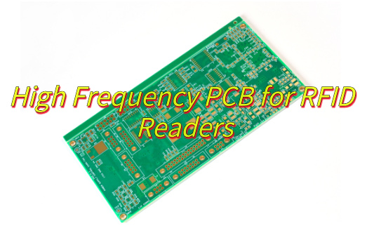
Why choose high frequency PCB for RFID readers? Let’s discover its benefits, applications, material selection, design technical parameter, design optimize solutions, recommended PCB manufacturer.
Are you worried about these problems?
How to select high frequency PCB board materials?
How to control high frequency PCB board processes?
How to balance cost vs lead time of high frequency PCB?
As a high frequency PCB manufacturer, EBest Circuit (Best Technology) can provide services and solutions:
Low-loss Material Supply: Stocked PTFE/Rogers laminates ensure stable dielectric constant (Dk≤3.0), reducing signal loss by 40%+.
Precision Impedance Control:±0.02mm trace width tolerance maintains ≤5% impedance variation for flawless signal transmission.
Rapid-response Flexible Production: Prototypes in 5-7 days, bulk order lead time shortened by 30% with 15%+ cost optimization.
Welcome to contact us if you have any inquiry for high-frequency PCB board: sales@bestpcbs.com.
Breakthrough in Reading Distance: Adopting low-loss substrates like Rogers RO4350B reduces signal transmission loss by 40%, enabling UHF-band reading distances exceeding 12 meters, ideal for large-scale logistics and warehouse scanning.
Enhanced Anti-Interference Capability: Optimized microstrip layout and multi-layer shielding grounding meet ETSI EN 302 208 standards, improving signal stability by 60% in industrial electromagnetic environments.
High-Speed Signal Integrity: Precise 50Ω impedance matching and decoupling capacitor configurations ensure data transmission rates up to 100Mbps, guaranteeing rapid tag response.
Precision Manufacturing Process: 0.1mm line/space blind-buried via technology with ±5% copper plating thickness tolerance minimizes signal loss and enhances system reliability.
TCO Optimization Proven: Case studies like DHL show 35% improvement in asset tracking efficiency, 99.2% inventory accuracy, 28% reduction in 5-year maintenance costs, and an 18-month payback period.
5G IoT Compatibility: Supports sub-6GHz bands and millimeter-wave integration, complying with 3GPP Release 17 specifications for future smart logistics and autonomous driving scenarios.
Global Standard Compliance: Passes GS1 certification, IEEE 802.11 compatibility tests, and RoHS material requirements, ensuring seamless global market access.
Supplier Evaluation Framework: Structured assessment model covering material certification, process capability, testing validation, and case references, providing quantifiable decision-making tools for commercial conversion.
Applications of High Frequency PCB in RFID Readers
NFC Payment Terminals
Smart Access Control Systems
Industrial Sensor Networks
Large-scale logistics and warehouse scanning
Smart retail shelf management
Real-time medical equipment tracking
Contactless vehicle passage in transportation
Industrial automation production line control
Smart city infrastructure monitoring
Cold chain logistics temperature tracking
How to Choose High Frequency PCB Material for RFID Readers?
1. Three Key Parameters
Low Dk (≤3.6, e.g., Rogers RO4350B Dk=3.48) reduces signal delay; PTFE (Dk=2.1) suits UHF/mmWave for faster transmission.
Low Df (≤0.004, e.g., RO4350B Df=0.0037) minimizes signal loss; PTFE (Df=0.001) ensures 5G/6G signal integrity.
High Tg (≥150°C, e.g., RO4350B Tg=280°C) resists heat; PTFE handles -260°C~260°C for extreme conditions.
2. Scenario-Specific Matching
UHF (900MHz) uses RO4000 series (low cost, easy processing); 5G/mmWave (24GHz+) selects PTFE (low loss) or ceramic-filled materials (high stability).
Humid environments choose PTFE (water absorption ≤0.02%); high-temperature scenarios use PI (Tg≥260°C); anti-metal interference requires multi-layer shielding grounding.
3. Cost-Process Balance
Mid-frequency (≤10GHz) prefers RO4000 series (40% cheaper than PTFE); high-frequency (≥10GHz) uses PTFE (superior performance but 3-5x costlier).
RO4000 works with FR4 processes (lower equipment investment); PTFE needs specialized tools for precision needs.
4. EMC Compliance Essentials
Optimized microstrip lines + multi-layer shielding (meets ETSI EN 302 208) suppress 900MHz interference; decoupling capacitors near chip pins ensure clean power.
Prioritize GS1/IEEE 802.11/RoHS-certified materials; suppliers must provide impedance matching and signal integrity reports.
5. Validation Loop
Test read distance/anti-interference in real scenarios such as logistics, medical to verify performance.
Evaluate suppliers’ material certifications (e.g., Rogers authorization), process capabilities (blind/buried via yield ≥98%), and case references for reliable supply chain.
High Frequency PCB Board Design Technical Parameter
How to Design High-Frequency PCBs to Optimize the Reading Distance of RFID Readers?
1. Antenna Size & Polarization Optimization
Size Scaling: 86×54mm large-size tags achieve 12m read range in industrial scenarios (260% improvement vs 35×35mm tags), suitable for large object identification like warehouse pallets.
Circular Polarization: Spiral/microstrip patch antennas support random tag orientation, improving detection rate from 75% to 98% in logistics sorting.
Metal Clearance: Maintain ≥10cm spacing between antenna and metal objects; optimized layout reduces read range attenuation by 40% in metal-adjacent scenarios.
2. Low-Loss Material Selection
Material Comparison: Rogers RO4350B (Dk=3.48/Df=0.0037) reduces signal attenuation by 40% vs FR4 for UHF; Taconic TLY-5 (Dk=2.2/Df=0.002) excels in millimeter-wave for 5G integration.
Moisture Management: PTFE substrates with ≤0.02% water absorption require waterproof coatings or low-absorption materials in humid environments.
3. Stack-Up & Impedance Control
6-Layer Structure: TOP (RF signal)-GND-Inner signal-Power-GND-BOTTOM (mmWave signal) ensures tight coupling between signal layers and ground planes, reducing crosstalk.
Smith Chart Matching: LC/π-networks achieve 50Ω matching, improving sensitivity by 2-3dB and restoring ≥3.2m read range in metal environments.
Calibration: S-parameter testing ensures tuning accuracy; dynamic tuning algorithms adapt to impedance fluctuations from tag position changes.
Anti-Metal Solutions: Ceramic substrates or absorptive adhesive tags with FHSS combat EM interference, maintaining 99% recognition rates on metal surfaces.
6. Environmental Robustness Enhancements
Liquid Compensation: Dielectric constant compensation reduces signal attenuation; phased-array antennas minimize 89% blind spots in liquid container detection.
Thermal Stability: Materials with Tg≥150℃ (e.g., RO4350B Tg=280℃) operate in -40℃~150℃ environments, preventing layer separation or performance degradation.
Mechanical Optimization: 2oz copper thickness and thermal vias enhance PCB durability against vibration/impact in logistics.
7. System-Level Dynamic Optimization
Power Adaptation: 0.5W-2W dynamic regulation increases tag recognition from 200 to 800 per read, optimizing multi-tag concurrency.
Q-Value Anti-Collision: Machine learning predicts optimal read windows, boosting dynamic scene recognition by 40% and reducing missed tags.
Thermal Management: High-thermal-conductivity materials (e.g., copper substrates) with thermal vias dissipate heat from high-frequency power loss, ensuring stable operation and extended lifespan.
Why Choose EBest Circuit (Best Technology) as High Frequency PCB Manufacturer?
19 Years of Expertise: 19-year focus on high-frequency PCBs with 5,000+ validated projects. Unique process knowledge base and failure analysis system reduce defect rates by 60% vs industry average.
Quality Certification: ISO9001/IATF16949/ISO13485 certified, make sure that every process passed ISO quality inspection system.
5-7 Days Rapid Prototyping: 5-7 Days prototype delivery for standard high-frequency PCBs; 3-5 Days turnaround for urgent orders. Supports 180+ global regions with 99.2% on-time delivery for urgent R&D needs.
Advanced Material: Uses low-loss materials like Rogers RO4350B and Taconic TLY-5 (Dk=2.2-3.48, Df=0.0004-0.0037) with dielectric constant tolerance ≤±0.02, reducing signal loss by 40% vs FR4.
Precision Process Control: High-precision CNC drilling, laser cutting, and automated lines ensure ±0.01mm line width/spacing and ±5% impedance matching accuracy for 50Ω/75Ω standards.
Cost Advantage: Eco-friendly high-frequency materials cut costs by 40%. Tiered pricing: double-layer boards as low as ¥0.8/piece; six-layer boards under ¥220/m², 30% cheaper than imports.
Reliability Testing: Endures -40°C to 125°C thermal cycling, humidity shock, and signal loss optimization. Maintains stability in extreme environments (such as space simulation, industrial radar) with <0.1% error rate.
Turnkey Solutions: Full-service support from circuit design and BOM sourcing to PCB assembly. Reduces overall cycle time by 50% with rapid customization response.
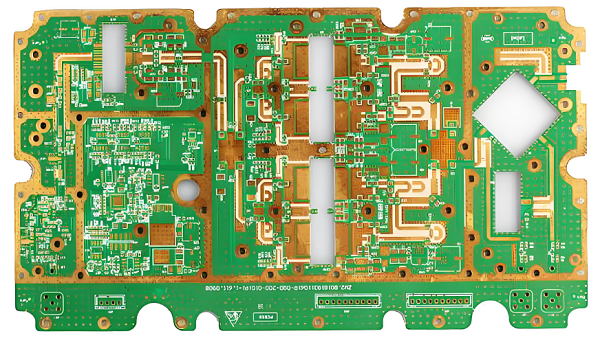
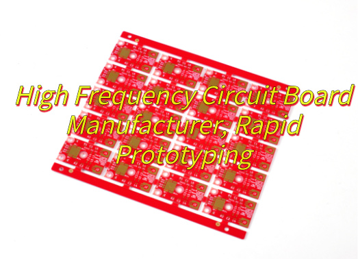
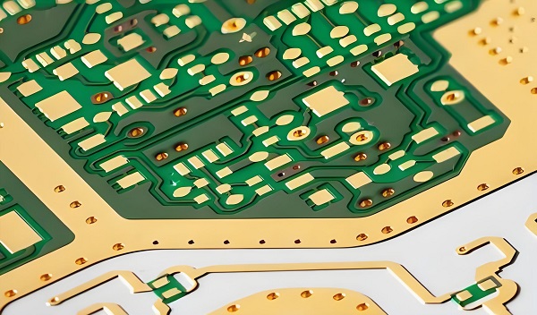
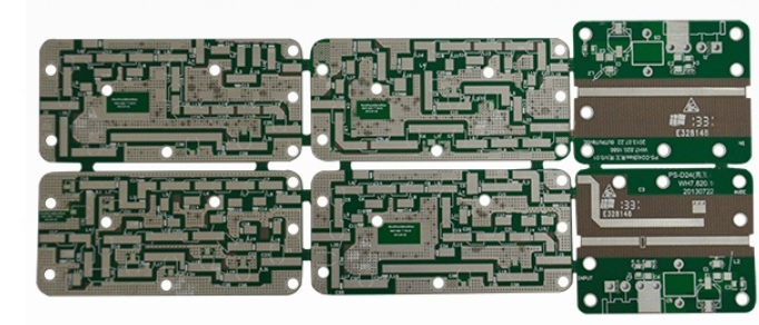
Here is a photo of high frequency PCB we did before:
What is high frequency circuit board? Let’s discover its material, technical parameter, design guideline, production processes and recommended manufacturer.
Are you troubled with these issues?
Is phase distortion caused by unstable Dk/Df in your high-frequency design?
How to reduce HF material costs without compromising performance?
How to ensure material consistency from prototype to mass production?
As a high frequency PCB manufacturer, EBest Circuit (Best Technology) can provide you service and solution:
Full-band Dk±0.02 Control: Phase error <1° across 24-77GHz, eliminating signal distortion.
High Frequency Circuit Board is a printed circuit board specifically designed to handle high-frequency signals (such as RF, microwave, and high-speed digital signals). Its core features include the use of low dielectric loss materials (e.g., PTFE, ceramic-filled substrates) and optimized layout design to achieve low signal attenuation, high signal integrity, and stable electromagnetic performance. This meets the stringent requirements of high-speed transmission and low noise in high-frequency scenarios such as 5G communications, radar systems, and satellite equipment.
What is the Best Material for High Frequency Circuit Board?
Frequency Range: 2.4GHz (Wi-Fi routers), 5GHz (5G base stations), millimeter wave (radar/satellite communications), different frequency bands correspond to different transmission characteristics;
Power Level: High-power scenarios (>10W PA modules) require enhanced thermal design using metal substrates or thermal via arrays;
Interface Standard: PCIe 4.0 (16GT/s data rate), HDMI 2.1 (48Gbps bandwidth), USB 3.2 (20Gbps rate), ensuring interface compatibility and signal integrity;
2. Material Selection & Stackup Design
Material Type: PTFE substrate (Dk≈2.2, Df≈0.002, suitable for high-frequency), ceramic-filled substrate (Dk≈3.0-10, Df≤0.001, high-power scenarios), high-speed FR4 (Dk≈3.66, Df≈0.008, cost-sensitive);
Stackup Design: Signal layer-ground layer-power layer alternating arrangement, high-frequency signal layers adjacent to ground layers to reduce crosstalk, ground layers must be continuous without splits;
Dielectric Thickness: Thin dielectrics (3-5mil) for high-frequency bands (>10GHz, e.g., RO4350B), 8-12mil for mid/low-frequency;
Copper Thickness: ≥1oz (35μm) for high-frequency signal layers to reduce loss, ≥2oz (70μm) for ground layers to enhance heat dissipation, power layers adjusted based on current requirements.
3. Layout Planning & Component Placement
Components: RF modules (e.g., LNA, PA) placed near antennas to minimize transmission loss, high-speed chips (e.g., FPGA, CPU) placed near connectors to shorten signal paths;
Signal Path: Minimize length of high-frequency signal lines, avoid 90-degree corners (use 135-degree or curved routing), serpentine routing compensates DDR clock line timing deviations (length matching error ≤5mil);
Thermal Management: Thermal vias (≥10mil diameter) under high-power components or metal substrates (e.g., Aluminum PCB) to prevent hotspots;
EMC: Sensitive components (e.g., crystals) kept away from noise sources (e.g., switching power supplies), high-frequency regions isolated with dedicated power supplies and filtering capacitors.
4. Routing Design & Impedance Control
Differential Pair: Impedance strictly controlled at 100Ω (e.g., USB 3.0/PCIe), trace width/spacing ratio 1:1 (e.g., 5mil/5mil), length matching error ≤5mil;
Microstrip/Stripline: 50Ω RF signal lines (trace width ≈8mil, dielectric thickness ≈5mil), 75Ω video signal lines (trace width ≈12mil), high-frequency lines avoid crossing split planes;
Minimum Trace Spacing: ≥3× trace width (e.g., 5mil trace width requires ≥15mil spacing) to suppress crosstalk, high-frequency line spacing ≥λ/10 (e.g., 5GHz signal λ=60mm, spacing ≥6mm);
Crossing Split Planes: High-frequency signal lines crossing split planes bridged via capacitors or vias to reduce reflections/radiation.
5. EMC Optimization
Ground Via: Array spacing ≤λ/10 (e.g., 5GHz signal λ=60mm, via spacing ≤6mm) for low-impedance ground paths;
Shielding Structure: Metal cavities (thickness ≥0.2mm) or shielding layers (copper foil + conductive adhesive) to suppress resonances and electromagnetic radiation, high-frequency regions shielded independently;
Decoupling Capacitor: 0.1μF (high-frequency) + 10μF (low-frequency) paralleled near power pins (≤5mm) to reduce power noise;
Filter: LC filters (e.g., π-network) suppress power noise, ferrite beads absorb high-frequency noise for signal purity.
6. Simulation Verification & Iteration
Frequency Domain Simulation: ADS/HFSS analyze S-parameters (return loss ≤-10dB, insertion loss ≤1dB), radiation patterns (antenna optimization);
Time Domain Simulation: SIwave/Altium verify signal integrity (eye diagram openness ≥80%, crosstalk ≤5%) for high-speed digital signals;
3D EM Simulation: CST Microwave Studio evaluates antenna performance, radiation leakage, and coupling effects to optimize layout/shielding;
Iteration: Adjust layout/routing (e.g., add shielding, optimize impedance) based on simulation results until performance metrics are met.
7. Manufacturing Process Control & Testing
Lamination Process: Precise control of dielectric thickness (tolerance ≤±5%) to avoid delamination and bubbles;
Drilling Process: Microvia (0.15mm) copper plating uniformity (thickness variation ≤10%) to prevent via wall fractures and conductivity issues;
Impedance Testing: TDR verifies impedance matching (error ≤±5%) for signal quality;
Eye Diagram Testing: High-speed digital signal eye diagram analysis (eye height ≥800mV, eye width ≥80%UI), radiation scanning (anechoic chamber) confirms EMI compliance to regulatory standards.
How to Make a High Frequency Circuit Board?
1. Material Cutting & Selection: Select low-loss substrates (e.g., PTFE, ceramic-filled substrates), cut panels to design specifications, ensure clean edges without burrs to prevent stress cracks or signal transmission loss in subsequent processes.
2. Inner Layer Pattern Transfer: Use high-precision exposure machine (resolution ≤5μm) for inner layer pattern transfer, precisely remove excess copper with alkaline etching solution, control line width/spacing tolerance within ±10μm to ensure high-frequency signal path accuracy.
3. Lamination & Stacking: Stack multilayer boards and perform vacuum lamination, strictly control temperature (180-200℃) and pressure (300-500PSI) profiles to avoid interlayer bubbles or uneven dielectric thickness, ensuring impedance stability for high-frequency signal transmission.
4. Drilling & Plating: Use precision drill bit (hole diameter tolerance ±2μm) for through-hole/blind via drilling, control copper plating uniformity (thickness variation ≤10%) to prevent via cracking or conductivity issues, ensuring high-quality vertical interconnection for high-frequency signals.
5. Outer Layer Pattern Transfer: After copper plating thickening, transfer outer layer patterns, optimize line width/spacing (e.g., 50Ω microstrip requires precise matching of dielectric thickness and copper thickness) using impedance calculation software to ensure consistent impedance for high-frequency signal transmission.
6. Solder Mask Application: Apply liquid photo-imageable solder mask ink, form protective layer through exposure/development, reduce signal transmission loss and surface contamination, avoid excessive solder mask thickness affecting high-frequency signal radiation efficiency.
7. Surface Finish: Apply ENIG (Electroless Nickel Immersion Gold) or OSP (Organic Solderability Preservative) surface finish to enhance solderability and long-term reliability, prevent oxidation affecting high-frequency signal conductivity, ensuring solder joint quality and product longevity.
8. Testing & Verification: Perform TDR (Time Domain Reflectometry) for impedance matching (error ≤±5%), eye diagram analysis (eye height/width meets standards), radiation scanning (anechoic chamber testing for EMI compliance) to ensure high-frequency signal integrity and regulatory adherence.
9. Packaging & Shipping: Vacuum-pack for moisture/dust protection, include quality inspection report and material certificate (e.g., Dk/Df test data), ensure safe transportation and traceability, maintaining high-frequency PCB performance stability in real-world applications.
Why Choose EBest Circuit (Best Technology) as High Frequency Circuit Board Manufacturer?
19-Year High Frequency PCB Manufacturing Expertise – Specialized in PTFE/hydrocarbon processing with core technologies (microvias, buried blind holes, hybrid pressing). Completed 5,000+ High Frequency PCBprojects across 5G/radar/satellite.
Certified Quality System – ISO 9001/14001/IATF 16949 certified, RoHS/REACH compliant. Regular customer/third-party audits maintain system effectiveness.
Transparent Pricing & Cost Optimization – Leverage bulk procurement for raw material savings and lean production to minimize waste. Tiered pricing ensures industry-leading competitiveness with no hidden fees.
48-72 Hours Rapid Prototyping – Mature production lines + smart scheduling enable 7-10 day standard delivery, with urgent orders achievable in 2-3 days. Optimized supply chain ensures project timelines.
Full-Cycle Technical Support – Free DFM analysis, in-process optimization, and post-sales troubleshooting. 24/7 engineer team resolves issues within 48 hours.
Strict Quality Control – Raw material inspection, in-process IPQC, final AOI, environmental testing, impedance microsection, and third-party audits. Defect rate <0.3% surpasses industry norms.
Customization Flexibility – Supports any-layer HDI design, custom impedance (50Ω±2%), finishes (ENIG/OSP), and thicknesses (0.1-3.0mm) for tailored solutions.
Experience-Driven Problem Solving – 19-year fault database enables rapid diagnosis of common issues (e.g., signal loss, layer misalignment) with solutions to accelerate time-to-market.
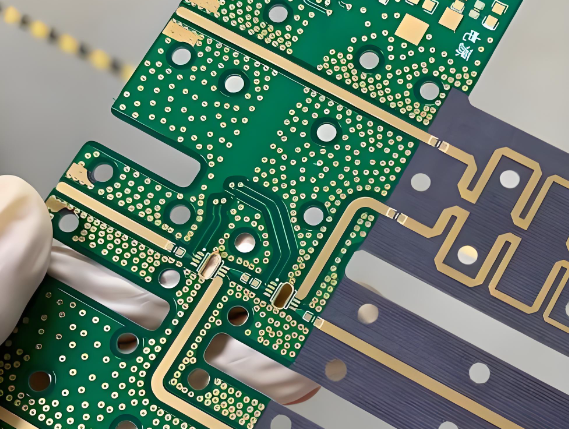
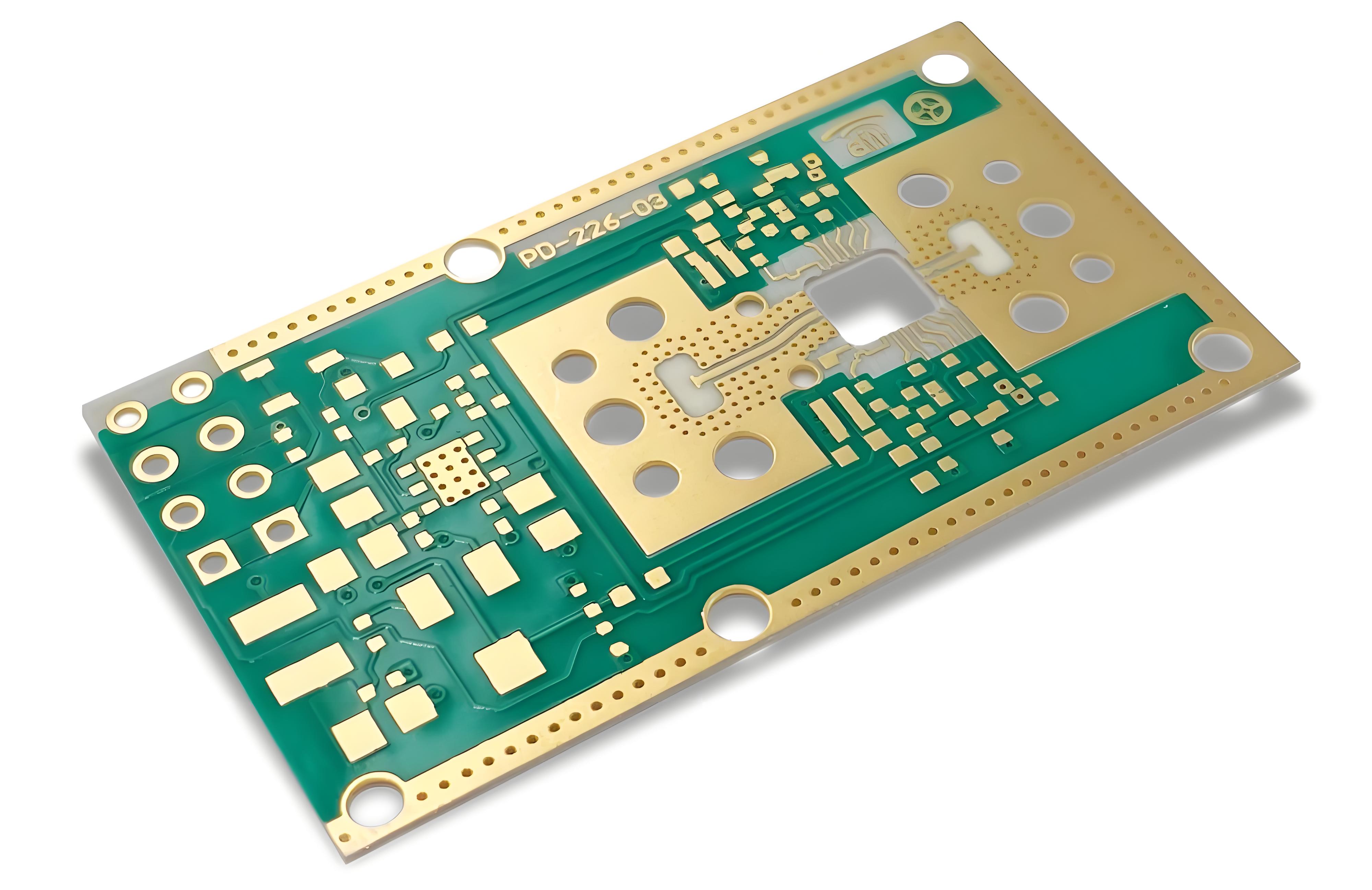
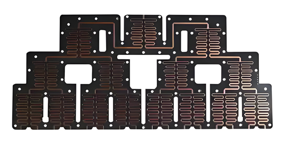
Below is a photo of high frequency high frequency circuit board we made before:
Our High Frequency PCB Capabilities
Base material:
Rogers/Telfon
Board Thickness:
0.5mm~3.0mm(0.02″~0.12″)
Copper thickness:
0.5 OZ, 1.0 OZ, 2.0 OZ, 3.0 OZ
Outline:
Routing, punching, V-Cut
Soldermask:
White/Black/Blue/Green/Red Oil
Legend/Silkscreen Color:
Black/White
Surface finishing:
Immersion Gold, HASL, OSP
Max Panel size:
600*500mm(23.62″*19.68″)
Packing:
Vacuum/Plastic bag
Samples L/T:
7~9 Days
MP L/T:
8~10 Days
How to Get a Quote for Your Project?
List of materials required for quotation:
Gerber files: Complete hierarchical data to ensure the design is complete.
Design files: Original files in Altium/OrCAD format, reproducing layout details.
BOM: Clearly specify component model, package, quantity, and supplier.
Technical parameters: Dimensions, number of layers, line width/space, aperture, and board thickness.
Material and process: Substrate type (e.g., PTFE), surface finish (ENIG), and copper thickness.
Impedance requirements: Target value (e.g., 50Ω) and signal integrity indicators.
Testing standards: Acceptance criteria such as impedance, eye diagrams, and radiation scans.
Quantity and delivery: Order size and expected delivery time.
PCB board with high frequency laminate is a specialized printed circuit board designed to handle signals in the GHz range with minimal loss. Unlike standard FR-4 boards, it uses advanced laminate materials such as PTFE, ceramic-filled PTFE, or hydrocarbon composites to ensure low dielectric constant and low dissipation factor.
These properties allow the board to deliver stable electrical performance, maintain signal integrity, and reduce electromagnetic interference. High-frequency PCBs are essential in applications like 5G networks, radar systems, satellite communication, and RF devices, where even small signal distortions can impact overall performance.
Are you curious about EBest Circuit (Best Technology)’s pcb board with high frequency laminate?
What is the maximum operating frequency and substrate type for high-frequency boards?
What substrate/copper foil thicknesses are supported?
What is the standard lead time?
EBest Circuit (Best Technology)’s pcb board with high frequency laminate can answer these questions.
High-frequency boards use Rogers or Telfon substrates, and their frequencies typically range from 300MHz to 3GHz.
Supported substrate thicknesses range from 0.5mm to 3.0mm (0.02″ to 0.12″), and copper foil thicknesses include 0.5oz, 1.0oz, 2.0oz, and 3.0oz.
Sample delivery time is 7-9 days, and mass production (MP) lead time is 8-10 days.
What is the best PCB material for high-frequency?
Selecting the right PCB material is critical for high-frequency performance. It determines signal integrity, stability, and overall reliability. High-frequency circuits demand materials with low dielectric loss, stable thermal behavior, and minimal signal distortion.
The most popular materials for high-frequency boards include:
PTFE (Polytetrafluoroethylene): Known for its low dielectric constant and excellent signal transmission.
Rogers Laminates: A trusted brand offering laminates like RO3000 and RO4000 series for RF and high-speed designs.
Ceramic-Filled PTFE: Provides improved mechanical strength and thermal performance compared to standard PTFE.
Hydrocarbon Laminates: Offer a balance of cost-effectiveness and electrical properties for mid-frequency designs.
Each option has its benefits. PTFE remains the top choice for the highest frequency designs due to its superior electrical characteristics.
Hydrocarbon laminates are often chosen when cost and performance need balance. They work well for mid-range frequency designs while keeping costs lower than pure PTFE boards. The best material depends on your application.
Which materials have the highest frequency?
For extreme frequency applications, materials must maintain stable electrical characteristics under high speed. The dielectric constant (Dk) and dissipation factor (Df) must be low and consistent across the operating range.
Rogers RO3003: Excellent for frequencies above 10 GHz.
Taconic RF Series: Offers stable electrical performance for RF applications.
Arlon Laminates: Known for thermal reliability and consistent performance.
These materials minimize signal degradation even at very high frequencies, making them essential for satellite, radar, and 5G applications.
Choosing these advanced laminates ensures your PCB can handle frequencies beyond 20 GHz without signal degradation.
What is considered high-frequency in PCB?
The term high-frequency refers to boards that handle signals above 300 MHz. However, in most cases, it applies to frequencies in the GHz range.
Digital systems often reach 50 MHz to 1 GHz. RF circuits start from 300MHz and go beyond 3 GHz. Microwave applications typically work between 20 GHz and 100 GHz.
As frequencies increase, material choice and design accuracy become more critical. Even minor variations in dielectric constant can cause signal delays or losses.
For designs above 1 GHz, standard FR-4 material is not suitable. High-frequency laminates are necessary to maintain performance and minimize interference.
What is the highest frequency PCB?
The highest frequency PCBs can support signals over 100 GHz. These boards are used in radar systems, satellite communication, and advanced wireless technologies.
Such boards require:
Ultra-low Dk and Df materials
Precise impedance control
Advanced fabrication processes
PTFE-based laminates combined with ceramic fillers remain the standard for these extreme-frequency applications. Manufacturing these boards demands strict process control. Small errors in thickness or copper roughness can affect performance significantly.
What is lamination in PCB?
Lamination is the process of bonding copper layers to dielectric materials under heat and pressure. It forms the multilayer structure of a PCB.
In high-frequency boards, lamination is even more critical. It must ensure consistent thickness, strong adhesion, and zero defects.
The process affects electrical performance, especially impedance control. Incorrect lamination can cause air gaps or uneven layers, which impact signal transmission.
High-quality lamination keeps your board reliable under high-speed operation. It ensures smooth copper surfaces, accurate layer alignment, and long-term durability.
How to design a high-frequency PCB?
Designing a PCB board with high frequency laminate requires attention to detail. Here are the core steps:
1. Choose the Right Laminate
Select a material with low Dk, low Df, and stable thermal properties.
2. Control Impedance
Use proper trace widths and spacing to maintain impedance.
3. Reduce Crosstalk
Keep high-speed signals away from each other. Add ground planes when possible.
4. Minimize Signal Loss
Avoid unnecessary vias. Use smooth copper to reduce attenuation.
5. Consider Stack-Up
A well-planned layer stack-up improves performance and reduces EMI issues.
How to reduce electromagnetic interference in PCB?
Electromagnetic interference (EMI) can degrade the performance of high-frequency circuits. Here’s how to reduce it:
Add Ground Planes: They provide a return path and reduce noise.
Use Shielding: Metal enclosures or conductive coatings can block external interference.
Shorten Signal Paths: Long traces act as antennas and increase EMI.
Filter Power Lines: Use decoupling capacitors to reduce noise on power rails.
Maintain Proper Spacing: Keep noisy and sensitive components apart.
Following these steps ensures a clean signal and improves board reliability. These techniques keep your board stable and interference-free.
What is the difference between high-speed and high-frequency PCB?
High-speed and high-frequency PCBs are different, though often confused.
High-Speed PCB: Refers to fast digital signals with sharp rise times, typically in MHz or low GHz.
High-Frequency PCB: Focuses on RF and microwave signals, often above 1 GHz.
The main difference lies in signal type and frequency range. High-speed boards emphasize signal integrity for digital data, while high-frequency boards handle analog signals like RF transmissions.
When should you use high-frequency?
You should choose a high-frequency PCB when your application works in the GHz range. These boards are essential for wireless communication, radar, and RF systems.
Use high-frequency PCBs for devices like smartphones, Wi-Fi routers, and 5G base stations. They are also required in satellite equipment, medical imaging systems, and automotive radar.
Any application needing low signal loss, stable impedance, and consistent performance at high speed requires these boards.
Standard FR-4 materials cannot provide the stability needed at these frequencies. High-frequency laminates are the only reliable choice.
If you need expert solutions for high-frequency PCBs, contact us at sales@bestpcbs.com. Our team is ready to provide professional support and the best quality boards for your application.
Have you ever faced such problems when design a PCB that used in high speed application?
Is your high-speed design bleeding signal strength?
How to solve poor thermal management in high-frequency systems to ensure stability and reliability?
How to effectively suppress severeEMI and meet EMC standards in high-frequency circuits?
At EBest Circuit (Best Technology), we fabricate high frequency PCB that can solve these problems. We use:
High quality materials with low loss and better shielding performance.
Utilize ground via array, densely arranging ground vias around radiation sources such as microstrip lines to form a “wall”.
Design multi-layer boards and adopt dedicated ground layers through reasonable stack-up design, provide a complete reference ground plane for high-frequency signals.
High frequency PCBs are essential in applications such as automotive radar, aerospace communication, medical imaging, 5G and satellite systems. These boards must handle signals above 100 MHz and, in many cases, well into the GHz range. At such speeds, signal losses, impedance mismatches, and electromagnetic interference (EMI) can cause severe degradation. EBest Circuit (Best Technology), a leading expertise in high frequency pcb manufacturing, can help to optimize your design and manufacture such board for you!
What is a High Frequency PCB?
A high frequency PCB is a printed circuit board designed to transmit signals above 500 MHz, often extending into 10 GHz, 30 GHz, or even higher depending on the application. Some applications, like automotive radar, require PCBs that perform stably at 77 GHz or more.
These boards are not limited to one sector. They are used in:
Wireless base stations and antennas
Radar for defense and vehicles
Satellite communication modules
High-speed computing and servers
Precision medical imaging devices
The key challenge is that as frequency rises, signals become more vulnerable to losses, reflections, and interference. A standard FR4 PCB cannot handle these issues beyond a certain point, which is why high frequency laminates and designs are essential.
High Frequency PCB Material
The choice of material determines how well a PCB will perform in high frequency environments. Engineers usually evaluate three main parameters:
Dielectric Constant (Dk): This defines how signals propagate through the material. A stable, low Dk improves signal speed and reduces delay.
Dissipation Factor (Df): Also called the loss tangent, this defines how much energy is lost as heat. Lower values are better for long-distance signal transmission.
Thermal Performance: Materials must handle fluctuating temperatures without expansion or deformation, especially in aerospace and automotive environments.
Common Materials Used in High Frequency PCB
PTFE (Teflon-based laminates): Offers extremely low loss and stable dielectric properties. Perfect for microwave and RF circuits, though harder to process during manufacturing.
Rogers laminates: Popular choices like RO4350B and RO3003 are widely used in communication devices due to their balance between cost and performance.
Arlon and Taconic: Trusted for aerospace and military-grade systems.
Ceramic-filled PTFE: Combines the benefits of PTFE with improved thermal stability, suitable for radar and satellite applications.
FR4: Economical, but only practical for low GHz applications, as losses rise sharply at higher frequencies.
When comparing FR4 to Rogers or PTFE, the difference is like comparing regular tires to high-performance racing tires. Both work, but only one is built for extreme conditions.
What is the Best PCB Material for High Frequency?
The “best” material depends on the actual use case. For example:
Up to 3 GHz: Rogers RO4350B provides stable performance at a manageable cost, widely used in RF applications.
Microwave range (10–30 GHz): PTFE laminates such as Taconic TLY or Rogers RO3003 give superior low-loss performance.
5G antennas: Low Dk and Df materials like Rogers RO4835 are chosen for consistent performance in outdoor environments.
Automotive radar (77 GHz): Ceramic-filled PTFE materials are the only reliable solution due to their high thermal and frequency stability.
Cost also matters. PTFE offers the lowest insertion loss but requires advanced processing, increasing manufacturing cost. Rogers materials are easier to fabricate and balance cost and performance, which is why they are widely used.
High Frequency PCB Characteristics
High frequency PCBs stand out due to specific characteristics:
Stable dielectric constant across wide frequencies
Low signal loss
Thermal durability
Controlled impedance
Dimensional stability
These boards are engineered not just to survive but to deliver reliable, repeatable performance in demanding environments.
High Frequency PCB Design Guidelines
Designing a high frequency PCB is a delicate balance of precision, material choice, and layout strategy. Even small mistakes in design can cause significant signal loss, reflection, or interference at gigahertz frequencies. Below are the key guidelines that engineers follow to ensure high performance.
1. Controlled Impedance Design
At high frequencies, the impedance of each trace must be carefully calculated and maintained. Variations in trace width, thickness, or dielectric spacing can cause reflections and signal degradation. Designers usually rely on simulation software to calculate controlled impedance for microstrip, stripline, or coplanar waveguide structures. The target impedance is often 50Ω for single-ended signals or 100Ω for differential pairs.
2. Minimize Trace Lengths
Signal paths should be as short as possible. Long traces increase insertion loss, cause delay, and may introduce unwanted reflections. In applications like RF communication or 5G antennas, even small increases in trace length can degrade signal integrity significantly.
3. Reduce the Number of Vias
Each via acts as a small inductance and capacitance, which can reflect high-frequency signals. Limiting via usage and optimizing via placement is essential. When vias are unavoidable, designers often use via stitching or back-drilling techniques to reduce parasitic effects.
4. Ground Planes and Reference Layers
A continuous, solid ground plane beneath signal traces improves return paths and minimizes electromagnetic interference (EMI). Multiple ground planes can be used in multilayer boards to enhance shielding and reduce noise coupling. Proper stacking ensures that signal layers are adjacent to reference planes, which stabilizes impedance and improves signal quality.
5. Differential Pair Routing
Differential pairs are widely used in high-speed digital and RF circuits. These pairs carry complementary signals, which improves noise immunity and reduces crosstalk. Designers maintain strict control over trace spacing, length matching, and symmetry to preserve signal integrity.
6. Stack-Up Optimization
The stack-up, or layer arrangement, determines how signal layers, power planes, and ground planes interact. Proper stack-up design can reduce cross-talk, improve thermal management, and control impedance. High frequency PCBs often use hybrid stack-ups with PTFE or ceramic layers to balance performance and manufacturability.
Every decision—from material choice to trace width, via placement to ground plane configuration—directly impacts signal integrity. A high frequency PCB is not just about connecting components; it is about managing signals, controlling impedance, and reducing loss to ensure reliable, precise performance in the gigahertz range.
High Frequency PCB Manufacturer – EBest Circuit (Best Technology)
Not all manufacturers are capable of producing high frequency PCBs. Handling PTFE and ceramic materials requires different lamination temperatures, drilling techniques, and plating processes compared with FR4.
At EBest Circuit (Best Technology), we bring specialized expertise in:
Fabricating Rogers, Taconic, PTFE, and hybrid PCB stack-ups.
Maintaining strict dimensional tolerances for impedance control.
Advanced inspection to measure dielectric thickness, copper roughness, and loss factors.
End-to-end MES traceability to ensure every board can be tracked back to its source materials and processes.
This combination of material knowledge, certified systems, and engineering support makes EBest Circuit (Best Technology) a trusted partner for customers who need more than just a standard PCB.
Insertion Loss Comparisons of Common High Frequency PCB Constructions
Material
Frequency (10GHz)
Insertion Loss (dB/inch)
Notes
FR4
~10GHz
0.7 – 1.0 dB
High loss, not recommended
Rogers RO4350B
~10GHz
0.2 – 0.3 dB
Cost-effective, reliable
Rogers RO3003
~10GHz
0.1 – 0.15 dB
Excellent for microwave use
PTFE Ceramic
~10GHz
0.05 – 0.1 dB
Premium choice for radar/5G
This table clearly shows why FR4 is avoided for RF designs. At high GHz levels, FR4 can lose more than three times the signal strength compared with PTFE laminates.
High Speed vs High Frequency PCB – What is the Difference?
The terms “high speed” and “high frequency” are often confused, but they describe different challenges:
High Speed PCB: Concerned with digital signals, rise times, and data rates. Examples: DDR memory boards, data centers, and Ethernet.
High Frequency PCB: Concerned with analog and RF signals in the GHz range. Examples: radar, antennas, and satellite communication.
In practice, many designs overlap. For instance, a 5G base station board must support high-speed data processing and high-frequency RF transmission simultaneously. This is why engineers often require both high-speed and high-frequency design expertise.
Why Do We Need High Frequency?
High frequency PCBs enable many of the technologies that define modern life:
5G base stations and smartphones: Delivering ultra-fast, low-latency communication.
Automotive radar: Assisting advanced driver-assistance systems and autonomous driving.
Satellite communication: Providing global coverage for navigation and broadcasting.
Defense and aerospace: Supporting secure, high-performance radar and communication systems.
Medical devices: Enabling accurate imaging through MRI, CT, and ultrasound.
Without these boards, the next generation of communication and smart systems would not be possible.
Who Should Not Get High Frequency?
Not every project needs high frequency PCBs. For example:
A consumer product with simple sensors may not justify the extra cost.
Low-speed devices below 500 MHz can rely on FR4.
Cost-sensitive projects without high bandwidth needs should avoid high frequency laminates.
Choosing the right PCB type should always balance performance needs vs. budget.
FAQs
1. What frequency is considered high frequency in PCBs?
Any PCB designed to work above 500 MHz is typically considered high frequency, with advanced boards operating up to 60 GHz or more.
2. How does dielectric constant affect PCB performance?
A stable dielectric constant ensures signals propagate at predictable speeds and maintain impedance control, crucial for RF circuits.
3. Can FR4 be used for high frequency PCB?
FR4 works only up to around 1 GHz. Beyond that, losses become too high for reliable performance.
4. What are the challenges in manufacturing high frequency PCB?
Processing PTFE materials, achieving impedance accuracy, reducing insertion loss, and handling copper roughness are common challenges.
5. How to reduce signal loss in high frequency PCB design?
Use low-loss laminates, design shorter traces, avoid unnecessary vias, and apply smooth copper surfaces to reduce resistance.
Are you often curious about these questions about high frequency PCB?
Have you ever wondered why some electronic systems lose performance at higher frequencies?
Why a well-designed PCB for low-speed circuits often fails when pushed into GHz ranges?
How can designers minimize losses above 1 GHz?
The answer lies in the design of high frequency PCBs. High frequency PCBs also known as RF PCB or radio frequency pcb. They are more important in applications such as 5G, automotive radar, aerospace communication, medical imaging, and satellite systems. These boards must handle signals above 100 MHz and, in many cases, well into the GHz range. At such speeds, signal losses, impedance mismatches, and electromagnetic interference (EMI) can cause severe degradation.
This blog provides detailed guidelines for designing high frequency PCBs. From material selection to signal routing, impedance control, thermal management, and testing, we will walk through the critical factors engineers must consider.
What Frequency Range is Considered High Frequency in PCB Design?
In PCB engineering, high frequency generally refers to signal frequencies above 500 MHz. For RF and microwave circuits, the range extends from 1 GHz up to 100 GHz. Typical applications include:
Wi-Fi (2.4 GHz / 5 GHz)
Bluetooth (2.4 GHz)
5G NR bands (3.5 GHz / 28 GHz / 39 GHz)
Automotive radar (24 GHz / 77 GHz)
Satellite communication (Ku-band 12–18 GHz, Ka-band 26–40 GHz)
The higher the frequency, the more sensitive the PCB becomes to signal loss, dielectric constant stability, and copper surface roughness. For instance, at 28 GHz (5G mmWave), even 0.1 dB/cm of insertion loss can cause serious degradation in system performance.
What PCB Materials are used for High Frequency Applications?
The dielectric substrate is the foundation of high frequency PCB design. Key material properties include:
Dielectric Constant (Dk): Should remain stable across frequency and temperature.
Dissipation Factor (Df): Lower values mean lower signal loss.
Thermal Conductivity: Crucial for high-power RF designs.
Common Materials for High Frequency PCBs
Material Type
Dielectric Constant (Dk)
Dissipation Factor (Df) @10GHz
Thermal Conductivity (W/m·K)
Typical Use Case
FR4 (High Tg)
4.2–4.7
0.020–0.025
0.3
<1 GHz, low-cost boards
Rogers RO4350B
3.48 ±0.05
0.0037
0.69
2–20 GHz, antennas
Rogers RO3003
3.00 ±0.04
0.0013
0.50
mmWave 5G (28 GHz, 39 GHz)
Taconic RF-35
3.50
0.0018
0.62
Microwave circuits
PTFE (Teflon)
2.1–2.6
0.0009–0.0015
0.25–0.30
Aerospace, radar
Ceramic-filled PTFE
3.0–10
0.001–0.005
0.7–1.2
High-power RF
Data comparison shows that Rogers RO3003 has one of the lowest Df values, making it widely used in 5G mmWave base stations. PTFE-based laminates dominate satellite and radar applications where extreme performance is required.
How Does Dielectric Constant Affect Signal Speed?
The dielectric constant (Dk) directly influences the propagation velocity of signals on PCB traces. The relation is:
Where c = 3 × 10^8 m/s (speed of light in vacuum).
For FR4 (Dk ≈ 4.5) → v ≈ 1.41 × 10^8 m/s
For Rogers RO4350B (Dk ≈ 3.48) → v ≈ 1.61 × 10^8 m/s
For PTFE (Dk ≈ 2.2) → v ≈ 2.02 × 10^8 m/s
This means PTFE substrates allow signals to travel ~43% faster than FR4. In high-speed digital systems (like SerDes 56G PAM4 links), such differences greatly influence timing margins.
What are the Key Design Rules for High Frequency PCB Layout?
Designing high frequency boards requires stricter rules compared to conventional PCBs:
1. Controlled Impedance Traces
Single-ended 50 Ω, differential 90–100 Ω are typical.
Impedance tolerance must be within ±5% for frequencies above 10 GHz.
2. Insertion Loss Minimization
Use smooth copper foils (Ra < 2 μm).
Keep transmission lines short.
Avoid unnecessary vias, which can introduce 0.1–0.2 dB loss per via at 10 GHz.
Maintain spacing ≥3× trace width between high frequency lines.
Place sensitive analog circuits far from digital noise sources.
5. Thermal Management
For power amplifiers, substrates with >0.8 W/m·K thermal conductivity are recommended.
Use thermal vias under RF components for efficient heat dissipation.
How Thick should a High Frequency PCB be?
The thickness of the PCB substrate directly impacts impedance and signal integrity. Typical stack-up configurations:
PCB Thickness
Layer Count
Dielectric Thickness
Frequency Application
0.2–0.4 mm
2–4L
0.1 mm core
High-speed connectors, 10–20 GHz
0.6–0.8 mm
4–6L
0.2 mm core
2.4/5 GHz Wi-Fi, Bluetooth
1.0–1.6 mm
6–10L
0.3–0.5 mm core
Automotive radar, 24 GHz
2.0+ mm
8–12L
>0.5 mm core
28 GHz 5G, satellite boards
For example, in 77 GHz automotive radar PCBs, manufacturers often use 0.254 mm or thinner substrates to reduce dielectric loss and keep microstrip lines narrow enough for impedance control.
How to Reduce Signal Loss in High Frequency PCB Design?
Signal loss (attenuation) is one of the biggest concerns in high frequency circuits. It is affected by:
Conductor Loss: Surface roughness increases resistance at high frequencies due to skin effect.
Radiation Loss: Poor layout or sharp bends radiate energy.
Example of Insertion Loss Data
Material
Frequency
Line Length
Insertion Loss
FR4 (Df 0.020)
10 GHz
10 cm
-1.2 dB
Rogers RO4350B
10 GHz
10 cm
-0.25 dB
PTFE (Df 0.001)
10 GHz
10 cm
-0.05 dB
This demonstrates why high frequency applications almost never rely on standard FR4.
In Conclusion
Designing a high frequency PCB requires more than standard PCB know-how. From material selection to impedance control, routing, thermal management, and advanced testing, every step must be carefully engineered.
EBest Circuit (Best Technology) is a trusted PCB manufacturer in China with expertise in high frequency PCB fabrication. We offer advanced laminates like Rogers, Taconic, and Isola, alongside ISO9001, ISO13485, IATF16949, and AS9100D certifications. Our team applies rigorous quality control, competitive pricing, professional engineering support, and MES-based traceability to deliver reliable high frequency PCBs for industries such as 5G, automotive radar, medical devices, and aerospace.
If your project requires precise high frequency PCB solutions, EBest Circuit (Best Technology) is ready to provide professional guidance and manufacturing excellence.
FAQs
1. Can FR4 be used for high frequency PCBs?
Yes, but only for frequencies below ~1 GHz. For anything higher, specialized laminates are required.
2. What is the most commonly used material for 5G PCBs?
Rogers RO4350B and RO3003 are widely adopted due to their low loss at mmWave bands.
3. How do vias affect high frequency performance?
Each via can add 0.1–0.2 dB loss at 10 GHz, so designers minimize via count in RF paths.
4. Why is surface roughness important?
At high frequencies, the skin effect confines current to the outer conductor surface. Rough copper increases resistance and loss.
Rogers RT Duroid 5880 is a high-frequency laminate specifically designed for applications where precision and low signal loss are critical. The substrate is a composite material known for its excellent performance in RF and microwave circuits. It uses a PTFE (polytetrafluoroethylene) base reinforced with glass microfibers.
The use of glass microfiber ensures the material is durable but lightweight, making it suitable for applications in which weight is a factor. Its composition is perfect for projects where high-frequency signals are involved. From defense systems to automotive radar, RT Duroid 5880 is a reliable choice. It has become the go-to substrate for engineers and designers looking for efficiency, precision, and durability.
Composition of Rogers RT/duroid 5880
RT Duroid 5880 is composed of PTFE (polytetrafluoroethylene) combined with glass microfiber. PTFE provides a low dissipation factor, which reduces signal loss. This is important for maintaining high performance in RF and microwave applications. Glass microfiber reinforces the material, make it stronger without adding unnecessary weight. The composition also includes copper cladding, which is typically laminated on both sides. The copper layer helps with conductivity, ensuring signals travel efficiently across the board.
The unique combination of PTFE and glass microfiber gives RT Duroid 5880 its excellent mechanical stability. It also minimizes the effect of temperature changes, which is critical for high-frequency circuits. As a result, the material can handle extreme temperatures without affecting the performance of the PCB.
RT/duroid 5880 Specifications
The following table highlights the important specifications of Rogers RT Duroid 5880. These specs reflect the high performance of RT Duroid 5880 for complex RF and microwave tasks.
Property
Value
Dielectric Constant (Dk)
2.20 (±0.02)
Dissipation Factor (Df)
0.0004 (measured at 10 GHz)
Thermal Conductivity
0.20 W/m/K
Operating Temperature Range
-55°C to +150°C
Water Absorption
0.02%
Volume Resistivity
1.7 x 10^9 MΩ·cm (minimum)
Surface Resistivity
1.4 x 10^8 MΩ (minimum)
Coefficient of Thermal Expansion (CTE)
46 ppm/°C (in X-Y axis)
Tensile Strength
10.3 MPa
Flammability
UL 94 V-0
Peel Strength
5.0 N/mm (after soldering)
RT/duroid 5880 Thickness
RT Duroid 5880 comes in various thicknesses. Engineers can choose the right thickness depending on their project’s needs. Rogers RT/duroid 5880 laminate is commercially available in sheet stock and roll stock forms in a range of thicknesses. Here’s a list of the standard thicknesses available:
Available sheet sizes:
304.8 x 457.2 mm
457.2 x 609.6 mm
609.6 x 914.4 mm
Standard thickness:
0.127 mm (5 mils)
0.254 mm (10 mils)
0.381 mm (15 mils)
0.508 mm (20 mils)
0.787 mm (31 mils)
1.524 mm (60 mils)
3.175 mm (125 mils)
Available roll widths:
304.8 mm
609.6 mm
1219.2 mm
Standard roll length: 76.2 meters
Thickness range: 0.127 mm to 1.575 mm
RO5880 RF PCB Advantages
Rogers RT Duroid 5880 has a lot of strengths when used in RF and microwave PCB projects:
Minimal Signal Loss
With a low dissipation factor of 0.0004, it reduces signal loss, which is very helpful for high-frequency systems like radar or satellite communications.
Strong Stability
It holds up well under temperature changes and in humid environments, keeping circuits running smoothly even in tough conditions.
Reliable Electrical Properties
The dielectric constant of 2.20 remains stable over a range of frequencies. This helps keep circuits working consistently without interference or signal issues.
Heat Tolerance
It withstands heat up to 150°C, making it a good choice for systems that need to handle higher temperatures.
Low Moisture Absorption
With only 0.02% water absorption, the material works well in damp environments. Outdoor systems like antennas benefit from this.
Ease of Manufacturing
The material is easy to work with during production, which keeps costs lower and speeds up manufacturing.
Chemical Resistance
The PTFE base resists damage from chemicals and solvents, making the material last longer in harsh environments like aerospace and industrial applications.
Typical Applications of High-Frequency PCB
High-frequency PCBs built with Rogers RT Duroid 5880 serve important roles across many industries:
Aerospace – used in radar, satellite, and navigation systems, RT Duroid 5880 supports reliable communication and tracking, even in high-pressure environments.
Telecommunications – in mobile networks, base stations, and antennas, high-frequency PCBs help maintain clear and fast data transmission, supporting the backbone of communication systems.
Medical Devices – MRI machines, wireless health monitors, and other equipment use high-frequency PCBs to keep medical data accurate and systems working seamlessly.
Defense – communication gear, and electronic warfare systems.
Automotive Systems – advanced driver assistance systems (ADAS) and vehicle radar depend on high-frequency PCBs for real-time data, making roads safer for everyone.
Satellite Communication – RT Duroid 5880 is frequently used in satellite systems where strong signal transmission over long distances is crucial for communication networks.
Common-Used High Frequency PCB Materials in EBest Circuit (Best Technology)
At EBest Circuit (Best Technology), we use a range of top-quality materials for high-frequency PCBs, depending on the project’s needs. Some of the most popular materials include:
Material
Dielectric Constant (Dk)
Loss Tangent (Df)
Key Features
Rogers RO4003C
3.38
0.0027
Low loss, excellent thermal stability, ideal for RF applications.
Rogers RO4350
3.48
0.0043
Low loss, high thermal conductivity, suitable for microwave applications.
RT/Duroid RO5880
2.94
0.0037
Very low loss, excellent performance at high frequencies, good for multilayer designs.
N4000-13
3.0
0.009
Good thermal stability, low moisture absorption, designed for high-frequency applications.
Taconic RF-60A
6.15
0.0027
High dielectric constant, low loss, suitable for low-loss RF and microwave applications.
Each material brings different strengths for specific applications, giving you the best options for your project.
Discuss Your High Frequency PCB Project with Us Today
If you have a high-frequency PCB project in mind, reach out to us. We’re experienced in creating high-quality PCBs that meet your exact specifications. Whether you need RF, microwave, or other types of high-frequency boards, we’ll make sure your project runs smoothly. Contact us at sales@www.bestpcbs.com today, and we’ll help you turn your plans into reality.
What is High-Frequency PCBs? High frequency PCBs are specifically designed to operate at frequencies typically above 1GHz. These circuit boards play a crucial role in modern communication systems like satellite communications, radar, and wireless networks. The materials used in high-frequency PCBs are different from those in standard PCBs. While standard PCBs use FR4 material, high-frequency PCBs often require specialized materials like PTFE (Teflon) or Rogers material to reduce signal loss and improve overall performance.
The growing need for faster and more reliable communication across industries makes high-frequency PCBs essential for creating cutting-edge devices.
FR4 is the most widely used material in standard PCBs due to its affordability and adequate performance for general applications. However, when it comes to high-frequency operations, FR4 has its limitations. The material can handle frequencies up to about 1GHz, but beyond this range, its performance starts to degrade significantly. High-frequency signals experience increased signal loss, dielectric losses, and electromagnetic interference (EMI) due to FR4’s higher dielectric constant (around 4.5) and poor thermal properties.
The limitations make FR4 unsuitable for more advanced applications like high-speed telecommunications, radar systems, and modern wireless technologies where signals operate in the gigahertz range. When designing PCBs that require frequencies beyond 1GHz, alternative materials like PTFE (Teflon) or Rogers laminates are recommended to maintain signal integrity and reduce losses.
How Do You Make High-Frequency PCB?
Creating a high-frequency PCB involves a few additional considerations compared to standard PCB designs. First, the choice of materials is critical. PTFE, Rogers, and other high-performance laminates are commonly used to ensure the PCB can handle high-frequency signals. Next, the board’s thickness, trace width, and layout need to be carefully calculated to avoid impedance issues. The key process including:
1. Material Selection
The first step is choosing materials that can handle high-frequency signals. Materials like PTFE, Rogers, or ceramic substrates are commonly used because they have lower dielectric constants, low dissipation factors, and better thermal stability. These materials ensure minimal signal degradation.
2. Controlled Impedance
High-frequency signals are sensitive to variations in impedance. Controlled impedance design ensures that the trace impedance matches the signal’s requirements, preventing reflection and signal distortion. This involves calculating the width and spacing of the traces and ensuring consistent dielectric properties across layers.
3. Multi-layer PCB
Multi-layer boards are often necessary for high-frequency applications to separate signals and reduce cross-talk. Ground planes are typically added to lower electromagnetic interference (EMI) and provide better signal grounding.
4. Short and Direct Signal Paths
Keeping signal paths as short as possible helps minimize signal loss and prevents unwanted interference. Traces that are too long or involve sharp bends can introduce delay and noise.
5. Shielding
In some cases, shielding techniques can be employed to prevent interference from other electronic components. This can include grounded planes, copper shields, or even encapsulating certain areas of the PCB.
High-frequency PCB design often requires sophisticated simulation tools. Software such as Ansys or Altium Designer helps predict how signals will behave on the board, allowing for adjustments to be made before fabrication.
What is the Highest RF Frequency?
In communication circuits, radio frequency (RF) bands cover a wide range of frequencies, typically starting from 20kHz up to 300GHz. The highest RF frequency currently used in commercial applications ranges from 100GHz to 300GHz, categorized as millimeter waves. These frequencies are essential for high-speed data transmission in technologies like 5G, radar systems, and advanced satellite communication. While developing PCBs that can efficiently handle such frequencies can be challenging, material innovations have made it possible.
What Are Some Important Considerations When Designing a PCB Layout for High-Frequency Circuits?
Designing a PCB for high-frequency circuits demands a careful approach to ensure signal integrity. The first thing to consider is the dielectric material. As previously mentioned, materials like Rogers or PTFE are preferred because they offer lower dielectric loss, which is crucial at higher frequencies. Trace layout is another critical factor. The length and width of the traces must be calculated to maintain impedance control, ensuring that signals don’t get distorted as they travel through the board.
1. Signal Integrity and Trace Layout
The layout of traces is a critical consideration in high-frequency PCB design. To maintain signal integrity, traces should be kept as short and straight as possible. Long traces can introduce delay, noise, and signal degradation. Additionally, sharp corners in trace routing should be avoided because they can lead to signal reflection and impedance discontinuities. Rounded or 45-degree bends are preferable to right-angle corners, which can cause unwanted signal interference.
2. Ground Planes and Layer Stack-Up
A solid, continuous ground plane is one of the most effective ways to reduce noise and EMI in high-frequency PCBs. Ground planes provide a low-impedance path for return currents and act as shields to prevent electromagnetic radiation from affecting other components. For multi-layer PCBs, having dedicated power and ground planes in the stack-up helps reduce noise and improves overall signal integrity.
3. Via Management
Vias introduce small inductances into the signal path, which can become problematic in high-frequency circuits. High-frequency signals are particularly sensitive to these inductances, and excessive use of vias can degrade signal quality. Designers should minimize the number of vias in high-frequency signal paths and use smaller, controlled-depth vias like microvias or buried vias to reduce parasitic effects.
4. Signal Isolation
High-frequency circuits often involve both analog and digital signals, and proper isolation between these signals is critical to prevent interference. Digital signals tend to generate high levels of noise, which can interfere with sensitive analog signals. To avoid this, analog and digital components should be physically separated on the PCB, with separate ground planes if possible.
5. Power Distribution and Decoupling
Stable power distribution is necessary to ensure that high-frequency components operate without interruptions. A decoupling capacitor should be placed near the power supply pins of each active component to filter out high-frequency noise and maintain a steady voltage. Multiple capacitors of different values (e.g., 0.1µF and 10µF) can be used in parallel to filter noise over a wide frequency range.
How Do You Avoid High-Frequency Interference in PCB?
Interference is a common issue in high-frequency PCBs, but it can be managed with the right design techniques. The most effective way to avoid high-frequency interference is by using a dedicated ground plane. This plane acts as a shield, helping to reduce EMI and cross-talk between different parts of the circuit. Shielding can also be applied to individual traces or components that are more susceptible to interference.
Ground Planes
A continuous ground plane is one of the most effective ways to reduce high-frequency interference. It acts as a shield and prevents unwanted noise from penetrating the circuit. The use of multiple ground planes in multi-layer PCBs can also provide better signal grounding.
Signal Layer Segregation
Isolating analog and digital signals helps to reduce interference between them. Analog signals are more susceptible to noise, so they should be kept separate from high-frequency digital signals.
Shorter Traces
Keeping traces short and direct minimizes the potential for signal loss or delay, and helps maintain signal integrity. The longer the trace, the more likely it is to pick up unwanted noise.
Minimize Via Usage
Excessive use of vias can create points of discontinuity in the signal path, leading to reflections and noise. If vias are necessary, they should be placed strategically and sparingly.
EMI Shielding
In some cases, it may be necessary to use EMI shields around particularly sensitive areas of the PCB.
Decoupling Capacitors
Adding decoupling capacitors between the power supply and ground helps to filter out high-frequency noise and maintain a clean signal.
What is the Difference Between High-Speed and High-Frequency PCB?
Though they may seem similar, high-speed and high-frequency PCBs serve different purposes. High-speed PCBs are designed to handle fast data transmission speeds, often used in applications like computing and networking. These PCBs focus on minimizing delay and ensuring signals reach their destination without distortion.
On the other hand, high-frequency PCBs are specifically optimized for circuits operating at high frequencies, often in communication systems. The emphasis here is on maintaining signal integrity across a wide frequency range. While both high-speed and high-frequency PCBs share common design principles, such as controlled impedance and signal integrity, the challenges they face differ. High-speed PCBs focus more on data transmission, while high-frequency PCBs deal with RF signals and the challenges of maintaining signal strength at higher frequencies.
How Do You Fix Frequency Interference?
If your PCB is experiencing frequency interference, there are several methods to fix the problem. One common approach is to improve grounding by using a continuous ground plane. This helps shield signals from external noise and interference. You can also add shielding to specific components or traces that are particularly susceptible to interference.
Adding filters at key points in your circuit can help block unwanted frequencies. For instance, a low-pass filter allows only low-frequency signals to pass through, blocking higher-frequency interference. You can also reduce trace lengths and maintain clean, direct paths for high-frequency signals. Finally, proper isolation of analog and digital circuits is crucial to prevent noise from leaking into sensitive areas.