AMB Ceramic PCB is a high-performance ceramic substrate designed for power electronics that demand strong copper-to-ceramic bonding, efficient heat dissipation, and long-term reliability. At Best Technology, we provide custom AMB ceramic PCB solutions using Al2O3, AlN, and Si3N4 ceramic materials for customers in automotive, industrial, energy, rail transit, and high-power semiconductor industries.
If your project requires a substrate that can handle high current, thermal cycling, and harsh operating conditions, AMB PCB is a dependable choice.
Why Choose Best Technology for AMB Ceramic PCB?
At Best Technology (EBest Circuit), we provide advanced ceramic PCB solutions tailored for high-performance applications.
Our Strengths
- 20+ years of PCB and PCBA experience
- Support for Al2O3, AlN, and Si3N4 substrates
- Copper thickness up to 800 µm
- Strong expertise in power modules and thermal design
- Full turnkey service from PCB to assembly
- Certified with ISO 9001, ISO 13485, and IATF 16949
We work closely with engineers to optimize designs for manufacturability, reliability, and cost efficiency.
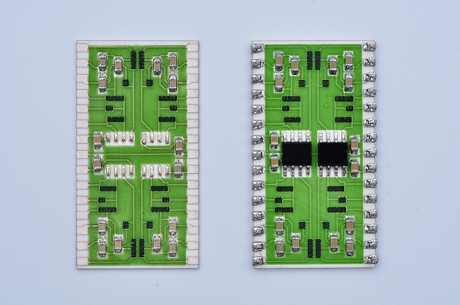
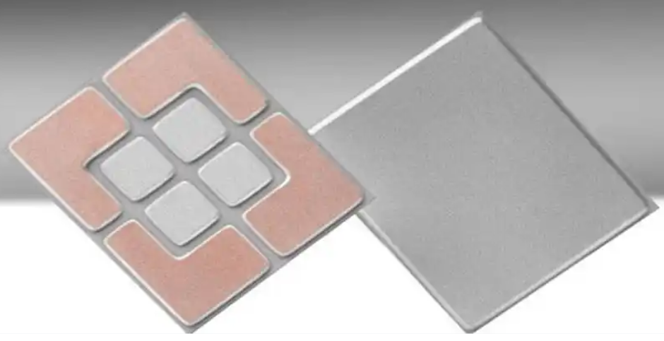
AMB Ceramic PCB
What Is AMB Ceramic PCB?
AMB stands for Active Metal Brazing. It is a ceramic substrate technology that bonds copper foil to ceramic by using active brazing materials containing metal elements such as titanium, silver, zirconium, or copper.
Unlike standard bonding methods, AMB creates a strong chemical bond between metal and ceramic at high temperature. This gives the finished substrate:
- Higher bonding strength
- Better resistance to thermal stress
- Excellent heat transfer performance
- Higher reliability in demanding environments
AMB ceramic PCB is widely used in power modules, IGBT modules, SiC packaging, EV systems, traction inverters, and renewable energy equipment.
Why Choose AMB Ceramic PCB?
For many power electronics projects, the substrate must do more than just carry traces. It must also help control heat, maintain insulation, and survive repeated thermal cycling. AMB ceramic PCB is chosen because it offers:
- Stronger Bonding Performance
The active metal brazing process creates a reliable bond between copper and ceramic, making the substrate more suitable for high-power module packaging.
- Better Reliability Under Thermal Stress
AMB substrates are designed for applications with frequent temperature changes and high operating loads. In advanced module structures, they can support very high thermal shock resistance.
- Excellent Heat Dissipation
With the right ceramic material, AMB PCB can provide strong thermal performance for power semiconductors, converters, and high-current designs.
- Good Match for Advanced Power Devices
AMB substrates are widely used with SiC chips, silver sintering processes, and thick copper designs, where both heat and reliability matter.
AMB Ceramic PCB vs DBC Ceramic PCB
Both AMB and DBC are used in ceramic substrate manufacturing, but they are not the same.
| Item | DBC Ceramic PCB | AMB Ceramic PCB |
| Bonding method | Direct bonding of copper to ceramic | Active metal brazing |
| Process structure | Simpler | More complex |
| Bonding strength | Good | Higher in many demanding applications |
| Thermal cycling reliability | Good | Excellent |
| Suitable for harsh environments | Yes | Better suited for severe conditions |
| Typical high-reliability use | Standard power modules | EV, traction, SiC, high-reliability power modules |
In short, DBC is a strong option for many standard power applications, while AMB is often preferred when stronger bonding and better long-term reliability are required.
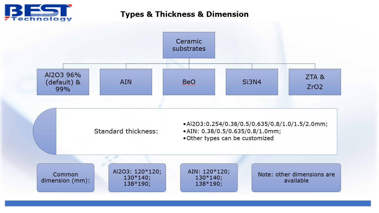
Ceramic Materials Available for AMB PCB
We provide AMB ceramic substrates based on different ceramic materials to match different power levels, cost targets, and reliability requirements.
1. Alumina AMB Ceramic PCB
Alumina is the most mature and cost-effective option.
Advantages:
- Lower material cost
- Stable supply
- Mature manufacturing route
- Good electrical insulation
Best for:
- Cost-sensitive projects
- Medium-power applications
- Products with moderate thermal requirements
2. Aluminum Nitride AMB Ceramic PCB
AlN offers very high thermal conductivity, making it ideal for fast heat transfer.
Advantages:
- High thermal conductivity
- Excellent heat spreading
- Suitable for high-power devices
Best for:
- High-current applications
- Power conversion systems
- Compact designs with high heat density
3. Silicon Nitride AMB Ceramic PCB
Si3N4 is the preferred material for projects that require both mechanical reliability and thermal performance.
Advantages:
- High bending strength
- Strong thermal shock resistance
- Thermal expansion closer to silicon
- Excellent reliability in demanding environments
Best for:
- Automotive power modules
- Traction systems
- Wind power converters
- High-reliability SiC and IGBT packaging
Material Property Comparison
| Item | Unit | Al2O3 | AlN | Si3N4 |
| Density | g/cm³ | 3.7 | 3.3 | 3.22 |
| Thermal conductivity | W/(m·K) | >20 | >170 | >80 |
| Coefficient of thermal expansion | ppm/°C | 6.9 | 4.7 | 2.5 |
| Bending strength | MPa | >350 | >350 | >700 |
| Dielectric constant | @1MHz | 9.8 | 9.0 | 8.0 |
| Breakdown strength | kV/mm | >15 | >20 | >20 |
Alumina AMB Ceramic PCB
Alumina ceramic PCB is the most mature and cost-effective option among AMB substrate materials.
Because alumina is widely available and easier to process, it is often used where budget control matters. The manufacturing base for alumina is also more established, which helps keep cost lower.
Advantages of Alumina AMB Substrates
- Mature production process
- Lower material cost
- Stable electrical insulation
- Good availability for volume production
Limitations of Alumina
The main limitation is its relatively low thermal conductivity. Compared with AlN and Si3N4, alumina transfers heat less efficiently. For that reason, it is more suitable for:
- Low to medium power applications
- Products with lower thermal load
- Systems with moderate reliability requirements
Aluminum Nitride AMB Ceramic PCB
Aluminum nitride ceramic PCB is known for its very high thermal conductivity. This makes it a strong option for electronic products that need fast heat removal. With thermal conductivity above 170 W/(m·K), AlN performs much better than alumina in heat dissipation. It is often selected for:
- High-power electronic devices
- High-current modules
- Power conversion systems
- Applications with limited space for heat spreading
Benefits of AlN AMB Substrates
- Excellent thermal conductivity
- Strong electrical insulation
- Good performance in high-power designs
- Better thermal management than alumina
Design Consideration
Although AlN performs very well thermally, its mechanical toughness is not as strong as silicon nitride. In repeated high and low temperature cycling, this can limit its service life in some harsh environments.
So while AlN is a very capable choice, it is usually best for applications where heat transfer is the top priority, but extreme mechanical shock resistance is not the main concern.
Silicon Nitride AMB Ceramic PCB
Silicon nitride ceramic PCB is often considered the premium choice for AMB applications that require both thermal performance and mechanical reliability.
Silicon nitride has a thermal conductivity above 90 W/(m·K) and a coefficient of thermal expansion very close to silicon. This helps reduce stress between the substrate and semiconductor chip during temperature changes.
It also offers very high bending strength, often above 700 MPa, which is much higher than alumina and AlN.
Why Si3N4 Stands Out
- High mechanical strength
- Good thermal conductivity
- Excellent thermal shock resistance
- Strong resistance to corrosion and oxidation
- Better long-term reliability in harsh environments
High thermal conductivity silicon nitride ceramics usually contain a large proportion of the stable β-Si3N4 phase, which contributes to stronger and more reliable performance.
Typical Applications of Si3N4 AMB PCB
- Automotive power modules
- Wind turbine converters
- Traction systems
- High-voltage DC transmission
- Power modules with partial discharge resistance requirements
In many advanced power systems, Si3N4 AMB substrates are selected when reliability matters just as much as heat dissipation.
Main Manufacturing Process of AMB Ceramic PCB
The manufacturing process of AMB ceramic PCB is more complex than standard PCB production because it combines ceramic processing, metal brazing, and precision patterning.
A typical AMB PCB production flow includes the following steps:
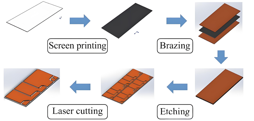
1. Ceramic substrate preparation
The ceramic sheet is cleaned and prepared for bonding.
2. Active metal brazing paste or filler application
A brazing material containing active metal elements is applied evenly to the ceramic surface.
3. Copper foil alignment
Copper foil is placed on the ceramic substrate.
4. High-temperature brazing
The assembly is heated under controlled conditions so the active metal reacts with the ceramic and forms a strong bond.
5. Cooling and bond stabilization
The bonded structure is cooled carefully to maintain flatness and bond quality.
6. Circuit pattern imaging
The copper layer is patterned according to the circuit design.
7. Etching
Copper is etched, and in AMB structures the extra solder layer may also need to be removed.
8. Surface finishing and inspection
The finished substrate goes through surface treatment, dimensional inspection, and reliability checks.
Because AMB products include an additional brazing layer, the production route is more demanding than DBC. However, this extra process is also what enables AMB to achieve stronger bonding and better reliability in many power module applications.
Main Features of AMB PCB
- High bonding strength between copper and ceramic
- Excellent thermal dissipation for high-power devices
- Strong thermal cycling reliability
- Good compatibility with SiC and other advanced semiconductors
- Stable electrical insulation under demanding conditions
- High mechanical durability, especially with silicon nitride
- Support for thick copper layers, in some cases up to 800 μm
- Suitable for high-voltage and high-current applications
Common Applications of AMB Ceramic PCB
- High-power semiconductor modules
- High-frequency switching devices
- Wind power systems
- Solar energy equipment
- Automotive electronics
- Locomotives and rail transportation
- Aerospace electronics
- IGBT modules
- 5G communication electronics
- Medical devices
- High-power LED lighting
- Industrial control equipment
- Defense and security systems
These applications often require a substrate that can operate under heat, vibration, current stress, and repeated thermal cycling without early failure.
Need a Reliable AMB Ceramic PCB Supplier?
If you are looking for an AMB ceramic PCB manufacturer for automotive, IGBT, SiC, renewable energy, or industrial power applications, Best Technology is ready to support your project.
Send us your design files or technical requirements, and our engineering team will review them and provide a suitable solution.
Email: sales@bestpcbs.com