High-quality PCB assembly Australia is pivotal for stable electronic product performance, blending precision manufacturing with adaptability to local industry needs. Professional PCB assembly Australia services adhere to regional regulatory standards and leverage stable local supply chains, streamlining production cycles and mitigating potential risks across projects of all sizes.

Why Choose PCB Assembly Australia?
- Compliance with local regulatory standards, ensuring products meet Australia’s electronic industry certifications and safety norms.
- Shorter supply chain distances, reducing shipping delays and logistics costs compared to offshore services.
- Real-time communication with manufacturers, facilitating quick adjustments to design or production requirements.
- Access to turnkey PCB assembly services Australia that cover design, prototyping, assembly and testing in one stop.
- Adherence to strict quality control protocols tailored to Australia’s industrial, medical and automotive sectors.
- Support for small-batch and prototype orders, meeting urgent project needs with fast turnaround.
- Local after-sales service, resolving assembly issues promptly without cross-border communication barriers.
- Alignment with environmental standards such as RoHS, ensuring eco-friendly production processes.
Top 10 PCB Assembly Manufacturer in Australia
| Company Name | Main Services | Core Strengths | PCBA Capabilities | Typical Lead Time |
| EBest Circuit Co., Limited | PCB design, prototyping, assembly, mass production | 20+ years of experience, free DFM review, global certification portfolio | SMT, through-hole assembly, IPC-A-610 Class 3 assembly, 98%+ yield rate | 24-hour prototyping, 7-14 days mass production |
| Hetech | Custom PCB design, prototyping, assembly, testing, turnkey solutions | Australian-based, 30+ years’ experience, automated SMT lines, AOI inspection, AS/NZS compliance | SMT/through-hole mixed assembly, high-reliability Class 3 assembly, defense/industrial compatibility | 2-4 days prototypes, 8-14 days mass production |
| QualiEco Circuits | PCB manufacturing, assembly, design support, mass production | Sydney-based factory, Electronex exhibition participant, strict quality control, RoHS compliance | Single/double/multi-layer PCB assembly, high-precision component placement, functional testing support | 3-6 days prototypes, 10-15 days mass production |
| GPC Electronics | PCB assembly, electronic contract manufacturing, testing/packaging | Australian registered, automated assembly equipment, multi-industry solutions | SMT assembly, high-density PCB processing, automotive/medical compatibility | 4-7 days prototypes, 9-16 days mass production |
| PCB Planet | PCB design, manufacturing, assembly, prototyping, technical support | Local professional service provider, high-quality solutions, real-time local communication | Single/double-panel assembly, small batch order compatibility, solder paste stencil support | 2-5 days prototypes, 7-12 days mass production |
| Emona Instruments Pty Ltd | PCB assembly, test equipment support, prototype validation | Australian Pty Ltd registered, Rigol equipment distributor, exhibition participant | SMT assembly, integrated testing services, education/industrial compatibility | 3-8 days prototypes, 11-18 days mass production |
| Altronic Distributors Pty Ltd | PCB assembly, component distribution, one-stop manufacturing | Leading Australian electronics service provider, stable local supply chain, ABN registered | Mixed technology assembly, component traceability, medium batch order compatibility | 4-6 days prototypes, 10-17 days mass production |
| Nordson DIMA Australia | PCB assembly, coating equipment support, precision assembly | Local equipment manufacturer, precision coating technology, comprehensive certifications | High-reliability PCB assembly, protective coating, automotive-grade compatibility | 5-7 days prototypes, 12-19 days mass production |
| Cirtech Australia | PCB manufacturing, assembly, prototyping, batch OEM | Established local manufacturer, Melbourne/Sydney dual bases, excellent reputation | Multi-layer PCB assembly, flexible circuit compatibility, harsh environment processing | 3-7 days prototypes, 8-15 days mass production |
| TechRentals Electronics | PCB assembly, test equipment rental, small batch services | Abundant local test resources, flexible small batch adaptation, rapid response | Prototype assembly, functional testing, small SMD component handling | 1-4 days urgent prototypes, 7-14 days small batch |
Quality Standards for PCB Assembly Australia
- ISO 9001:2015: Meet this quality management system standard to ensure consistent production quality and process control across all PCB assembly Australia projects.
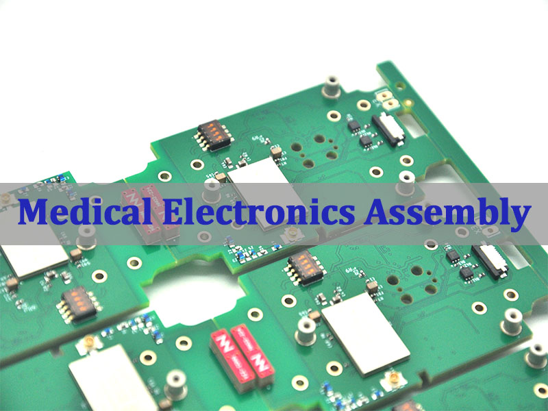
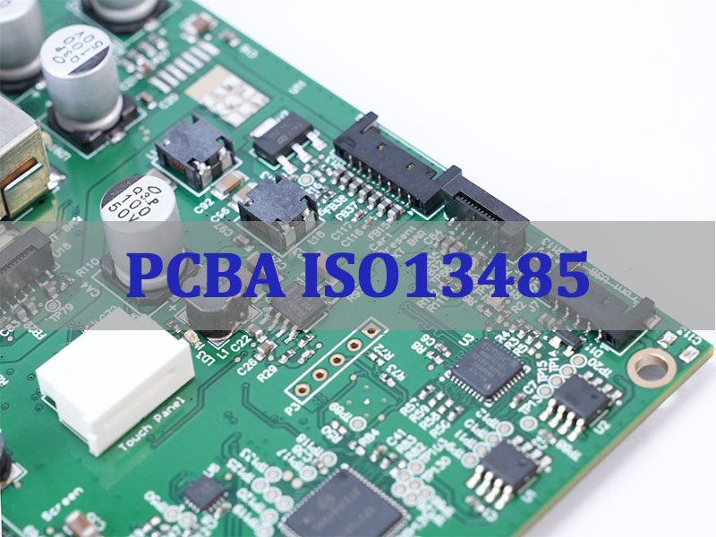
- ISO 13485:2016: Follow this standard for medical device-related PCB assembly Australia, ensuring compliance with healthcare industry quality and safety norms.
- IPC-A-610 Rev E Class 2/3: Comply with this electronic assembly acceptability standard, covering general and high-reliability applications like defense and aerospace.
- IPC-6012/IPC-6013: Adhere to IPC-6012 for rigid PCB manufacturing and IPC-6013 for flexible PCBs, ensuring structural and performance integrity.
- RoHS Directives: Comply with environmental regulations for eco-friendly component and material use, aligning with global and Australian sustainability requirements.
How to Choose the Best PCB Assembly Australia Service?
A Selection Guide to the Best PCB Assembly Manufacturer in Australia:
- Verify Target Certifications: Confirm whether the supplier holds ISO 9001 (quality management), ISO 13485 (medical), IATF 16949 (automotive), and IPC standard certifications. Prioritize suppliers compliant with Australian AS/NZS standards for better local market adaptation.
- Assess Technical Hardware and Precision: Inspect core equipment such as high-precision LDI exposure machines, automated SMT production lines, and AOI/X-ray inspection systems. Confirm their capability to handle fine-pitch components and multi-layer PCBs.
- Evaluate Industry Experience: Choose manufacturers with successful case studies in your specific field (defense, industrial, medical). Local PCB assembly companies with specialized expertise in Australia can mitigate adaptation risks.
- Verify Service Scope: Confirm they offer local Australian turnkey PCB assembly services, including component procurement, prototyping, testing, and packaging, to match your project scale.
- Review Supply Chain Stability: Inquire about component sourcing channels to ensure genuine parts. Local suppliers with redundant logistics plans are better equipped to handle delivery disruptions.
- Check Quality Control System: Ensure comprehensive IQC/IPQC/OQC inspections with a yield rate of over 98%. Request defect handling procedures to avoid rework delays.
- Confirm Pricing and Cost Transparency: Request a detailed quote including materials, assembly, testing, and logistics. Clearly define expedited service fees in advance to avoid hidden costs.
- Assess Technical Support: Prioritize suppliers offering free DFM review services and 24-hour technical support. Timely design adjustment support is crucial for prototype iterations.
- Review After-Sales Guarantee: Clarify warranty terms (at least 1-year warranty for bare boards) and efficiency in resolving quality issues. Local after-sales service avoids cross-border communication barriers.
- Check Delivery Reliability: Confirm written delivery time commitments and real-time production tracking. Choose suppliers who can flexibly accommodate urgent orders.
Types of PCB Assembly Services Australian PCBA Manufacturers Offered
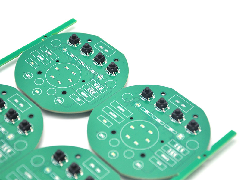
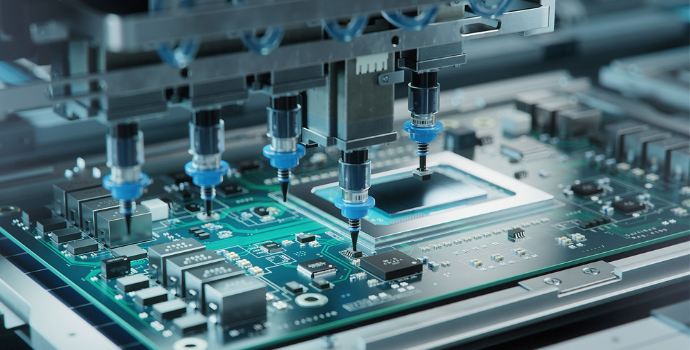
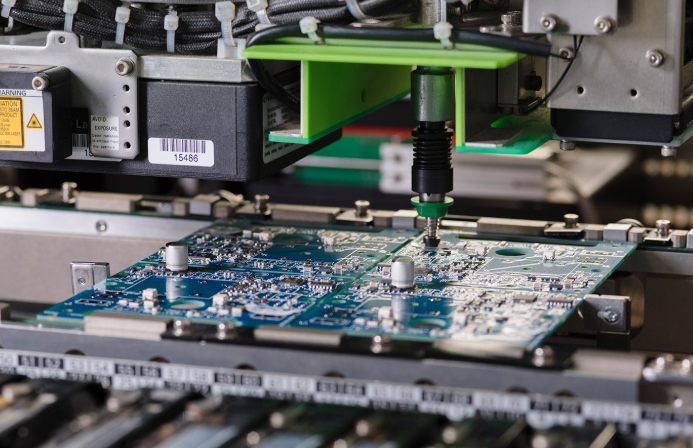
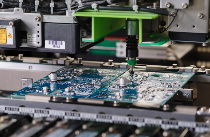
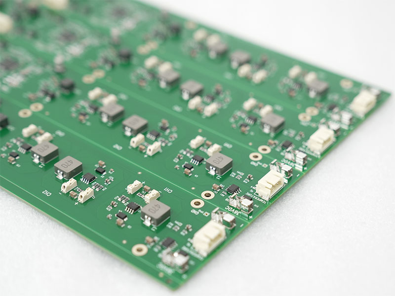
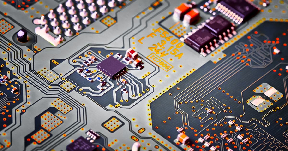
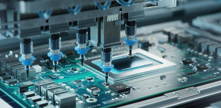
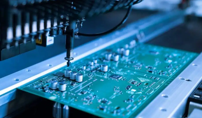
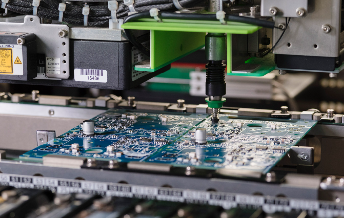
- SMT (Surface Mount Technology) Assembly: High-precision, high-density component placement for miniaturized products.
- Thru-Hole Assembly: Suitable for rugged components in industrial and automotive applications.
- Mixed Technology Assembly: Combined SMT and thru-hole processes for complex circuit requirements.
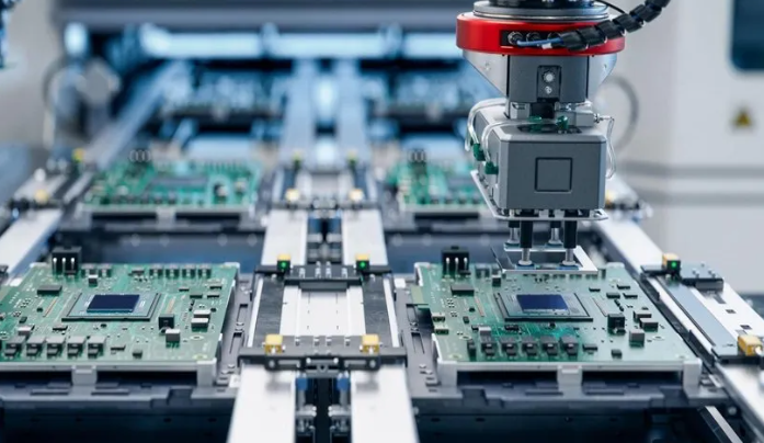
- Turnkey Assembly: End-to-end services from design, component sourcing to final testing and packaging.
- Prototype Assembly: Rapid small-batch production for design validation and testing.
How to Evaluate the Assembly Capability of PCB Assembly Companies in Australia?
Evaluation Guide to Assembly Capability of PCB Assembly Australia:
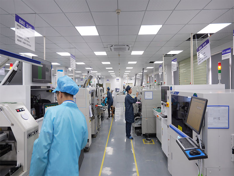
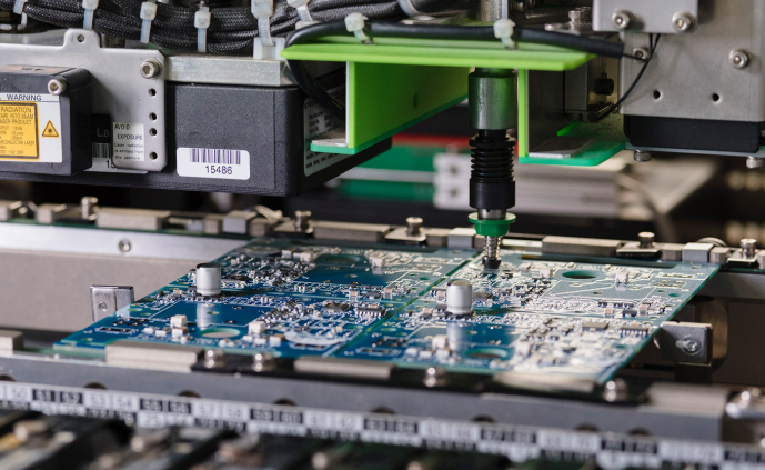
- Evaluate core equipment performance: Focus on automated pick-and-place machines (0.01mm+ positioning accuracy) and reflow ovens (±1℃ precision temperature control). These devices directly define the precision of PCB assembly service Australia and ensure stable component placement.
- Confirm process parameter limits: Inquire about key indicators like maximum PCB layer count (24+ layers preferred), minimum trace width (≤0.1mm) and hole diameter (≤0.2mm). These parameters determine if the manufacturer can handle your complex design requirements.
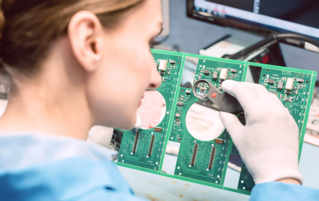
- Assess inspection system comprehensiveness: Ensure AOI inspection coverage hits 90%+ to minimize false positives. For BGA components, verify X-ray inspection capability; add functional testing to validate final product performance, forming a full-process quality barrier.
- Review mass production yield stability: Require a consistent 98%+ yield rate for batch orders. Ask for defect analysis reports, as they reflect the manufacturer’s mature quality control system for PCB assembly Australia.
- Verify component handling capacity: Confirm proficiency in processing tiny SMD parts (down to 01005 size) and specialized components (BGA, QFP, etc.). Anti-static measures for sensitive components are also a must to avoid damage during assembly.
- Conduct sample validation: Examine sample assemblies for solder joint integrity, component alignment and overall workmanship. Samples are the most intuitive way to verify the actual precision of a PCB assembly manufacturer in Australia.
- Check complex project experience: Inquire about past cases similar to your project (e.g., high-density boards, harsh environment applications). Request customer references to confirm the manufacturer’s practical capability in solving real-world problems.
How to Ensure the Lead Time of PCB Assembly Manufacturer in Australia?
Evaluation Guide to the Lead Time of PCB Assembly Manufacturer in Australia:
- Secure written lead time commitments: Clarify prototyping (2-7 days) and mass production (7-15 days) timelines in contracts, including milestone checkpoints (material arrival, assembly completion). Add penalty clauses for delays (e.g., 0.5% of order value per day) to bind PCB assembly manufacturer in Australia.
- Verify production scheduling flexibility: Inquire if urgent order adjustments (e.g., design tweaks, batch quantity changes) can be accommodated within 24 hours, and how scheduling adjustments affect the final delivery date without compromising quality.
- Audit supply chain stability: Prioritize manufacturers with ≥60% local component suppliers to avoid cross-border delays. Confirm key components (e.g., ICs, resistors) have 7-14 days of safety stock, reducing risks from supply disruptions.
- Clarify expedited service terms: Confirm availability of express services (e.g., 24-hour prototyping, 3-5 days mass production) with transparent pricing—typically a 20-50% premium. Ensure terms cover cost breakdown and service scope for time-sensitive PCB assembly Australia projects.
- Establish real-time tracking mechanisms: Require access to online systems that update production status (Preparation of materials, component placement, testing, and packaging) every 12 hours. Ask for daily progress reports for high-priority orders to monitor timelines proactively.
- Validate contingency plans: Inquire about backup measures for equipment failures (e.g., spare SMT lines with 4-hour activation time) and supply disruptions (e.g., alternative local suppliers with 48-hour delivery capability).
- Review historical delivery performance: Request data on on-time delivery rate (OTIF) over the past 6-12 months (target ≥98%). Check customer testimonials and 2-3 case studies to confirm how delays were handled in previous PCB assembly service Australia projects.
How to Estimate the Cost of PCB Assembly Australia?
- PCB Specifications: Layer count, size, material (FR-4 vs ceramic) and thickness impact base costs.
- Component Factors: Quantity, density, brand and rarity affect procurement and assembly costs.
- Assembly Complexity: SMT, thru-hole or mixed technology, and high-density placement increase costs.
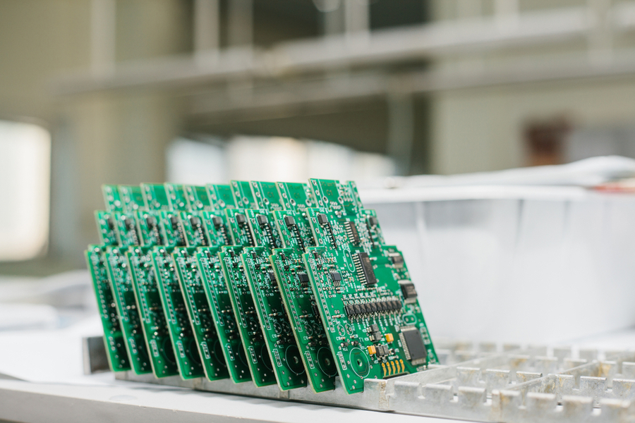
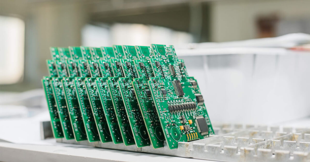
- Order Volume: Larger batches reduce unit costs, while small-batch/prototypes have higher per-unit rates.
- Surface Finish: HASL is cost-effective, while ENIG (gold plating) increases expenses for high-reliability needs.
- Testing Requirements: Additional tests (ICT, functional testing) add to overall costs.
- Lead Time: Expedited services typically incur 20-50% premium fees.
FAQs of PCB Manufacture and Assembly Australia
Q1: When ordering small-batch prototypes (20-50 units) from Australian manufacturers, the lead time is often longer than quoted. How to ensure on-time delivery of prototype PCBs?
A1: Prototype lead time delays often stem from unplanned production scheduling conflicts. Prioritize manufacturers that reserve dedicated prototype production lines, with a commitment to 2-4 day turnaround in writing. Confirm they maintain safety stock of common prototype materials (FR-4, standard solder paste) and offer real-time production tracking. This ensures timely delivery of PCB assembly Australia prototypes without compromising quality.
Q2: PCBs for industrial use in Australia fail EMC testing easily, leading to rework costs. What measures can prevent this during manufacturing?
A2: EMC failures are closely linked to design and process control. First, integrate DFM reviews focusing on EMC compliance, optimizing trace spacing (≥0.2mm) and ground plane design. Manufacture in line with AS/NZS CISPR standards, using low-noise materials and adding electromagnetic shielding layers if needed. Post-production EMC pre-testing is recommended to identify issues early, ensuring compliance for PCB manufacture and assembly Australia in industrial scenarios.
Q3: Solder joint oxidation frequently occurs on PCBs stored in Australia’s high-humidity environment. How to improve solder joint durability?
A3: Humidity-induced oxidation requires targeted material and process adjustments. Choose ENIG or immersion tin surface finishes instead of HASL, as they offer better corrosion resistance. During assembly, control workshop humidity (45-65%) and adopt nitrogen reflow soldering to reduce oxidation. Post-assembly, apply conformal coating (e.g., acrylic) to seal solder joints, enhancing durability for PCB assembly service Australia in humid conditions.
Q4: Australian manufacturers struggle to source rare components for custom PCB assembly, causing production delays. How to address this component shortage issue?
A4: Component shortages are mitigated by robust supply chain management. Select manufacturers with a local component database covering 60%+ common parts and a global backup network for rare components. Confirm they offer component substitution suggestions (with technical validation) and maintain 7-14 day safety stock for critical parts. This ensures uninterrupted PCB assembly manufacturer in Australia production for custom projects.
Q5: Multi-layer PCBs manufactured locally have inconsistent impedance, affecting signal transmission. How to ensure impedance control accuracy?
A5: Impedance inconsistency arises from material deviations and process errors. Use high-precision dielectric materials (FR-4 with stable Dk value) and strictly control copper thickness tolerance (±10%). Adopt LDI exposure technology for trace precision and conduct impedance testing on 5% of each batch (per IPC-6012 standards). Pre-production impedance simulation is also recommended to optimize design, ensuring signal integrity for high-reliability best PCB manufacture and assembly Australia.