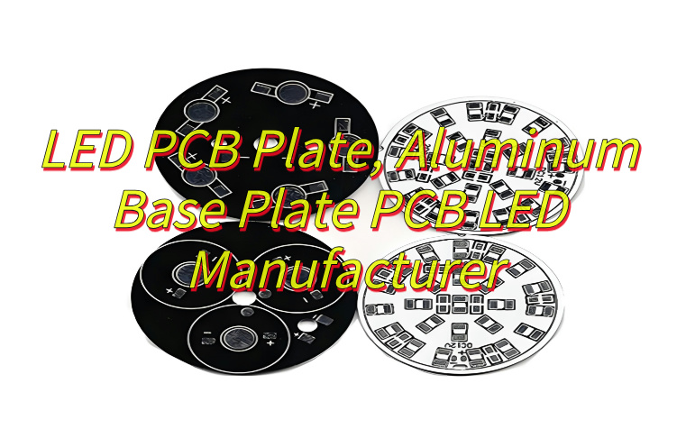
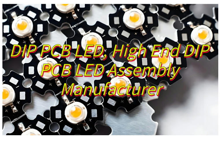
What is Sinkpad Copper Based PCB?
A sinkpad copper based PCB, also known as SinkPAD board or thermoelectric copper separation copper based PCB, is a specialized type of metal core printed circuit board. It mainly consists of two major parts: the top trace layer and the copper core/substrate. The top trace layer contains the electrical traces for the circuit, while the copper core serves as a heatsink.
A 1 – Layer SinkPAD board, a common type, consists of a copper circuit layer, a dielectric (non – conducting) layer, and a metal core/pedestal which is usually copper. It belongs to single – sided SinkPAD PCB and DTP (Direct Thermal Path) board, and is the most popular and cost – effective stack – up option with the fastest lead time.
Why Use Sinkpad Copper Based PCB?
Sinkpad copper based PCBs are used for several important reasons. After lamination, the electronics connection is on the trace layer, and the direct thermal conducting PAD comes from the copper core. The trace PAD on the trace layer is in the sink area of the copper core, which gives it the name “SinkPAD board”. This design allows for efficient thermoelectric separation.
These PCBs can reach a thermal conductivity of 400W/m.K. This high thermal conductivity is crucial in applications where heat dissipation is a major concern, such as in high – power LED lighting, power electronics, and other electronic devices that generate a significant amount of heat. By effectively dissipating heat, sinkpad copper based PCBs can improve the performance and reliability of electronic components and extend their lifespan.
Factors Affect the Price of Sinkpad MCPCB
- Material type (aluminum vs. copper)
The choice of material has a significant impact on the price of sinkpad MCPCB. Copper is generally more expensive than aluminum. Copper has excellent thermal conductivity, which is one of the key advantages for sinkpad PCBs as it helps in better heat dissipation. However, the higher cost of copper raw materials and the more complex processing requirements contribute to the increased price.
Aluminum, on the other hand, is a more cost – effective option. It has relatively good thermal conductivity and is lighter in weight. But its thermal performance is not as good as copper. When the application requires high – end thermal performance, copper is often the preferred choice, but it comes at a higher price.
- Board size and thickness
The size and thickness of the sinkpad copper based PCB also play a role in determining the price. Larger boards require more raw materials, such as copper and dielectric materials. Additionally, the manufacturing process for larger boards may be more complex, as it requires more precise alignment and processing steps.
Thicker boards also add to the cost. Thicker copper cores or additional layers of materials increase the material cost. Moreover, thicker boards may require more advanced manufacturing techniques to ensure proper electrical and thermal performance, which can drive up the production cost.
- Layer structure
The layer structure of the sinkpad PCB is another important factor. A more complex layer structure, such as multi – layer sinkpad PCBs, is more expensive than single – layer ones. Multi – layer PCBs require more manufacturing steps, including additional lamination processes, drilling for vias to connect different layers, and more precise alignment of the layers.
Each additional layer adds to the complexity and cost of the manufacturing process. For example, a 1 – Layer SinkPAD board is the simplest and most cost – effective option, while a PCB with multiple trace layers and copper core layers will be significantly more expensive.
- Order quantity
Order quantity has a direct impact on the price of sinkpad copper based PCBs. When the order quantity is large, the per – unit cost usually decreases. This is because manufacturers can take advantage of economies of scale. They can purchase raw materials in bulk at a lower cost, optimize their production processes, and reduce setup costs per unit.
For small – quantity orders, the fixed costs associated with setting up the production line, such as tooling costs and programming costs, are spread over a smaller number of units. As a result, the per – unit price is higher. So, customers who need a large number of sinkpad PCBs can often negotiate a better price per unit.
- Custom thermal pad design
Custom thermal pad designs can also increase the price of sinkpad copper based PCBs. Standard thermal pad designs are more cost – effective because they can be produced using existing manufacturing processes and tools. However, if a customer requires a custom thermal pad design, it may involve additional engineering work, such as designing new masks, adjusting the manufacturing process, and conducting additional testing.
Custom designs may also require special materials or manufacturing techniques to meet the specific thermal requirements. All these additional steps and requirements add to the overall cost of the PCB.
Sinkpad Copper Based PCB Applications
Sinkpad copper based PCBs have several common uses in the electronics industry:
- Thermoelectric separation applications:
Since the trace layer of SinkPAD boards is usually on the top side, they belong to single – sided SinkPAD PCBs and Direct Thermal Path (DTP) boards. This makes them suitable for applications where thermoelectric separation is required. For example, the SinkPad board provides excellent heat transfer from the LED to the base metal (copper) plate while maintaining excellent electrical isolation.
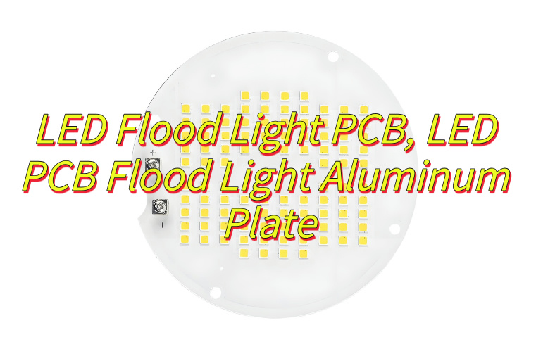
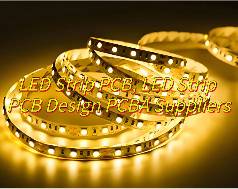
- High – power LED applications:
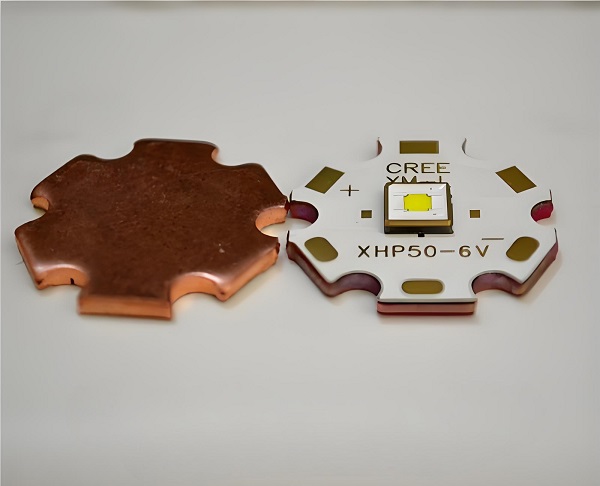
1 – Layer copper base SinkPad PCB: It can be used with surface mount and chip & wire components. The thermal PAD of the LED touches the convexity of the copper core/pedestal directly, achieving a thermal conductivity of 400W/m.K. The pad of the LED touches the copper base directly, allowing the heat generated by the LED to be dissipated quickly into the air or a heatsink, achieving the best heat dissipation and conduction.
2 – Layers copper base SinkPad PCB: It can also be used with surface mount and chip & wire components. Similar to the 1 – layer version, the thermal PAD of the LED touches the convexity of the copper core/pedestal directly, with a thermal conductivity of 400W/m.K.
In general, sinkpad copper based PCBs are used to provide superior thermal performance for medium – to high – power LEDs and other chips/components.
How Does A SinkPAD board Differ From A Traditional PCB?
A SinkPAD board is a special type of metal core PCB. In a SinkPAD board, the thermal conductive PAD is the convexity area of the copper core/pedestal, allowing the thermal PAD of the LED to touch the convexity area of the metal core directly. This enables the heat of the LED to be dissipated into the air much faster and more efficiently than a conventional PCB.
The SinkPad provides excellent heat transfer from the LED to the metal base plate/pedestal while maintaining excellent electrical isolation. The base copper base gives the board substrate mechanical integrity, distributes and transfers the heat to a heat sink, mounting surface, or directly to the ambient air.
In contrast, traditional PCBs do not have this direct thermal path feature. The heating of the LED in a SinkPAD board conducts directly into the copper core, which is different from the traditional thermal path. Due to this, a SinkPAD board can offer superior thermal performance for medium – to high – power LEDs or other chips/components.
How to Design a SinkPAD Board?
When designing a SinkPAD board, the following points need attention:
1. Panel layout design
If the board outline is not square or rectangle, the outline has to be made via CNC routing or Die – punching. While designing the panel layout, at least 2mm space between the edge of the SinkPAD board (SinkPAD PCB) should be kept in order for routing or Die – punching.
2. Routing and punching
Several layers of SinkPAD PCB will be routed together to save time. But for punching, there is only one layer of SinkPAD board (SinkPAD PCB) each time. Die – punching will be used only when there are big volume orders as the cost of die – punching tooling is higher compared with other ways.
Moreover, in the lamination process (laminate & align board before hot process lamination), after specific steps, the electronics connection will be on the trace layer and the direct thermal conducting PAD comes from the copper core. The trace PAD on the trace layer seems in the sink area of the copper core, which is how the SinkPAD board gets its name. And because the electronic – related function is on the trace layer and thermal conduction is on the copper core, they are separated from each other, so it is also named a Thermoelectric separation circuit board.
Your Trust Sinkpad PCB Supplier – EBest Circuit (Best Technology)
EBest Circuit (Best Technology) is a reliable supplier of sinkpad PCBs. We offer high – quality SinkPAD boards with excellent thermal performance. Our products are designed and manufactured using advanced techniques to ensure precise separation of the copper core and trace layers, resulting in efficient thermoelectric separation.
EBest Circuit (Best Technology) can provide various types of sinkpad PCBs, including 1 Layer SinkPAD boards, 2 layers sinkpad MCPCB and multi-layer sinkpad MCPCB, to meet different customer requirements. We also have the ability to handle custom designs, whether it’s a custom thermal pad design or a specific layer structure. With their expertise and experience in the field, customers can trust EBest Circuit (Best Technology) to deliver high – quality sinkpad copper based PCBs at a reasonable price.
Frequently Asked Questions
1. What is a double – sided SinkPAD board?
A double – sided SinkPAD board consists of at least one layer of circuit layer on both the top and bottom sides of the SinkPAD board, a dielectric (non – conducting) layer, and a metal core/pedestal which is normally copper. More components can be placed on this type of board, but engineers need to consider heat conduction.
2. What are the components of a 1 – layer SinkPAD board?
A 1 – layer SinkPAD board consists of a copper circuit layer, a dielectric (non – conducting) layer, and a metal core/pedestal which is usually copper. It belongs to single – sided SinkPAD PCB and DTP board and is the most popular and cost – effective option with the fastest lead time.
3. How is a 2 – layer SinkPAD board different from a 1 – layer one?
A 2 – layer SinkPAD board has two layers of circuit layer on the same side, along with a dielectric layer and a copper metal core/pedestal. It also belongs to single – sided SinkPAD PCB and DTP board. The main difference is that more traces can be placed on a 2 – layer SinkPAD board compared to a 1 – layer one.
4. What defines a multi – layer SinkPAD board?
Multi – layer SinkPAD refers to a metal core board that has more than 2 layers of trace circuits, either on the same side or on both the top and bottom sides, and has a direct thermal path (PAD). Examples include 4L SinkPAD board or 4L SinkPAD double – sided board.
5. What is the first step in the SinkPAD board manufacturing process?
The first step in the SinkPAD board manufacturing process is to prepare the manufacturing files. This involves separating the copper core and trace from one Gerber layer into two different layers. One layer will have only the trace without the center heatsink PAD of the LED (trace layer), and the other layer will have only the heatsink PAD (copper core layer).