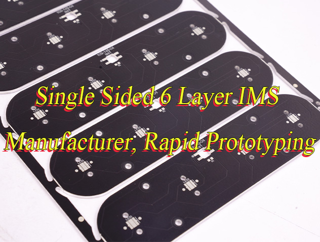
How to design a single sided 6 layer IMS? Let’s discover its benefits, applications, design spec and guideline, production process and manufacturer recommendation.
Are you troubled with these problems?
- Does significant crosstalk in 6-layer metal-based substrates due to electromagnetic shielding failure lead to yield decline in your products?
- Does uncontrolled thermal management in complex multi-layer IMS heat dissipation paths cause component performance degradation?
- Do frequent small-batch customization needs result in missed market opportunities due to lengthy traditional process cycles?
As a single sided 6 layer IMS Manufacturer, EBest Circuit (Best Technology) can provide you service and solution:
- Customized Metal-Based Material Formulation – Optimized dielectric constant for high-frequency scenarios, enhancing signal integrity tenfold to eliminate crosstalk.
- Micro-Via Array Thermal Management Matrix – Precision-etched 3D heat dissipation networks enable precise temperature control at component level, reducing thermal failure risk by 70%.
- Modular Rapid Response System – 72-hour rapid prototyping with end-to-end visual tracking, ensuring small-batch needs are met without delay.
Welcome to contact us if you have any request for single sided 6 layer IMS: sales@bestpcbs.com.
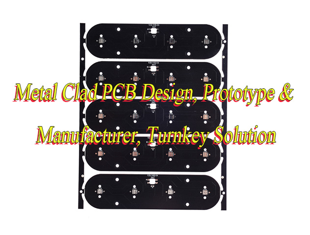
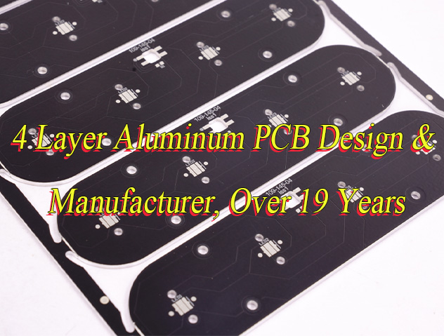
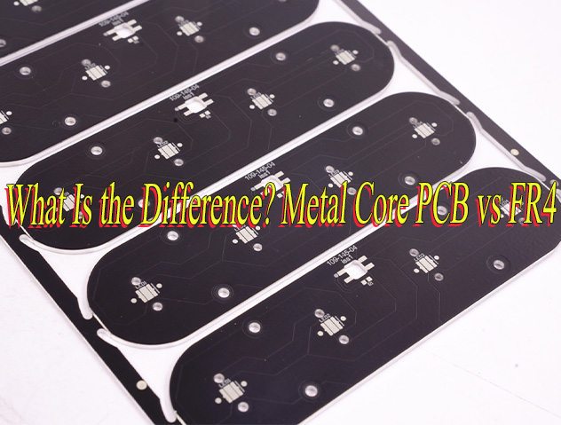
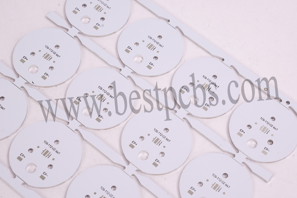
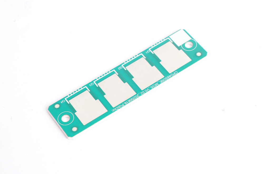
What Is A Single Sided 6 Layer IMS?
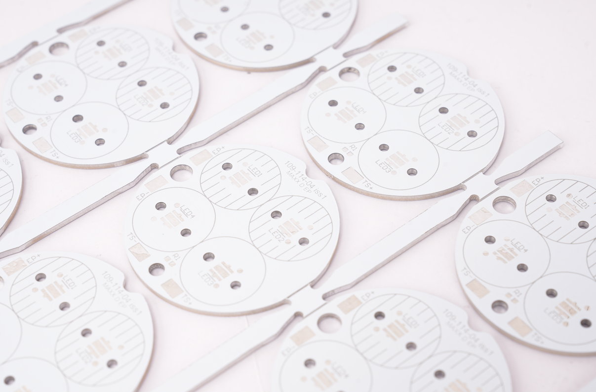
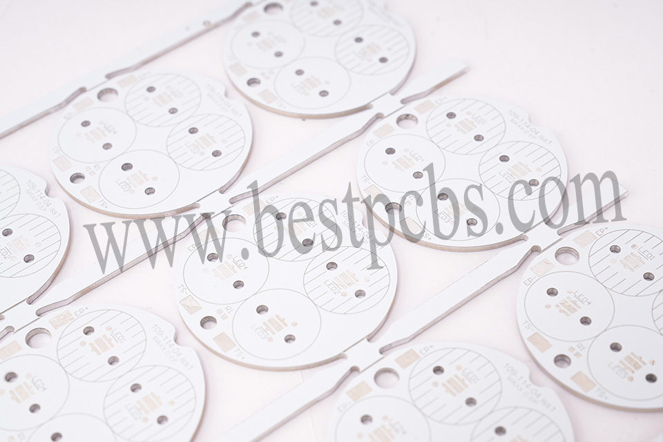
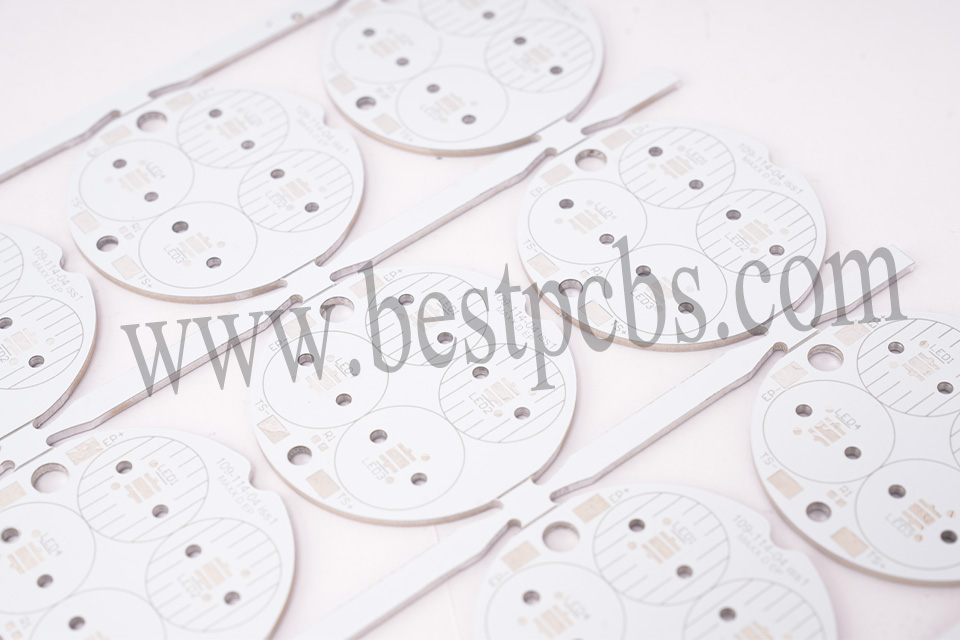
Single sided 6 layer IMS is a specially designed industrial metal substrate. Its core feature is the integration of an efficient metal (typically aluminum) heat dissipation layer with a multi-layer circuit structure.
Specifically, this substrate consists of six precisely laminated layers of distinct materials: at the base is a thick aluminum plate responsible for core heat dissipation; above the aluminum plate are multiple insulating dielectric layers and conductive layers (copper foil), designed such that all circuit traces are exclusively located on the top surface (single-sided) of the substrate, while the underlying aluminum plate remains intact for thermal conduction.
This structure retains the relative simplicity of traditional single-sided board wiring while significantly enhancing thermal dissipation capability and overall reliability through multi-layer insulating/conductive dielectrics and the underlying metal substrate. It is particularly suited for applications requiring rapid heat dissipation from high-power components with moderate circuit density requirements, such as high-power LED lighting, automotive electronics, and power modules.
What Are Benefits of Single Sided 6-Layer IMS?
- Enhanced Thermal Performance Extends Lifespan: Thermal prepreg materials achieve 8-12 times the conductivity of FR4, reducing thermal resistance to 1/100 of FR4. This minimizes component aging in high-power LED and automotive electronics, extending product lifespan by over 30% while lowering maintenance costs.
- Simplified Single-Layer Wiring Design: All circuit routing is concentrated on the top layer, with the bottom layer retaining a full aluminum heat sink. This avoids complex multi-layer wiring, cuts design cycles by 20%, reduces rework from wiring errors, and lowers costs for power modules with moderate circuit density.
- Multi-Layer Structure Boosts Reliability: Combining metal substrate with multi-layer insulation/conductive layers maintains single-layer wiring simplicity while improving insulation and thermal management. Automotive electronics show 40% lower failure rates with enhanced voltage fluctuation resistance for stable operation in harsh conditions.
- Full Lifecycle Cost Reduction: Improved heat dissipation reduces reliance on additional cooling components, cutting material costs by 15-20%. Efficient thermal management decreases maintenance frequency, lowering total operation/maintenance costs by over 25% for continuous-use scenarios like power modules.
- Broad Scenario Adaptability Enhances Competitiveness: Precisely matches high-heat-dissipation needs in high-power LED lighting, automotive electronics, and industrial power supplies. Rapid heat conduction ensures stable performance in high-temperature outdoor environments for smart grid devices, meeting demands for high reliability and long lifespan.
What Are Applications of Single Sided 6 Layer IMS?
- Aerospace: Satellite Communication Power Module, Spacecraft Thermal Control System Circuit Board.
- Defense Industry: Radar Transmitter Power Amplifier.
- New Energy Vehicles: Motor Controller Main Power Module, On-Board Charger (OBC) Core Circuit.
- High-End Medical: CT Machine X-ray Generator, High-Frequency Electrosurgical Equipment Power Supply.
- Industrial Control: High-Power Inverter Drive Board, Industrial Laser Pump Source Control.
- Semiconductor Manufacturing: Wafer Test Probe Card Interface Board, Chip Programming Equipment Power Module.
- Rail Transit: Train Traction Converter Control Board, Vehicle Auxiliary Power Module.
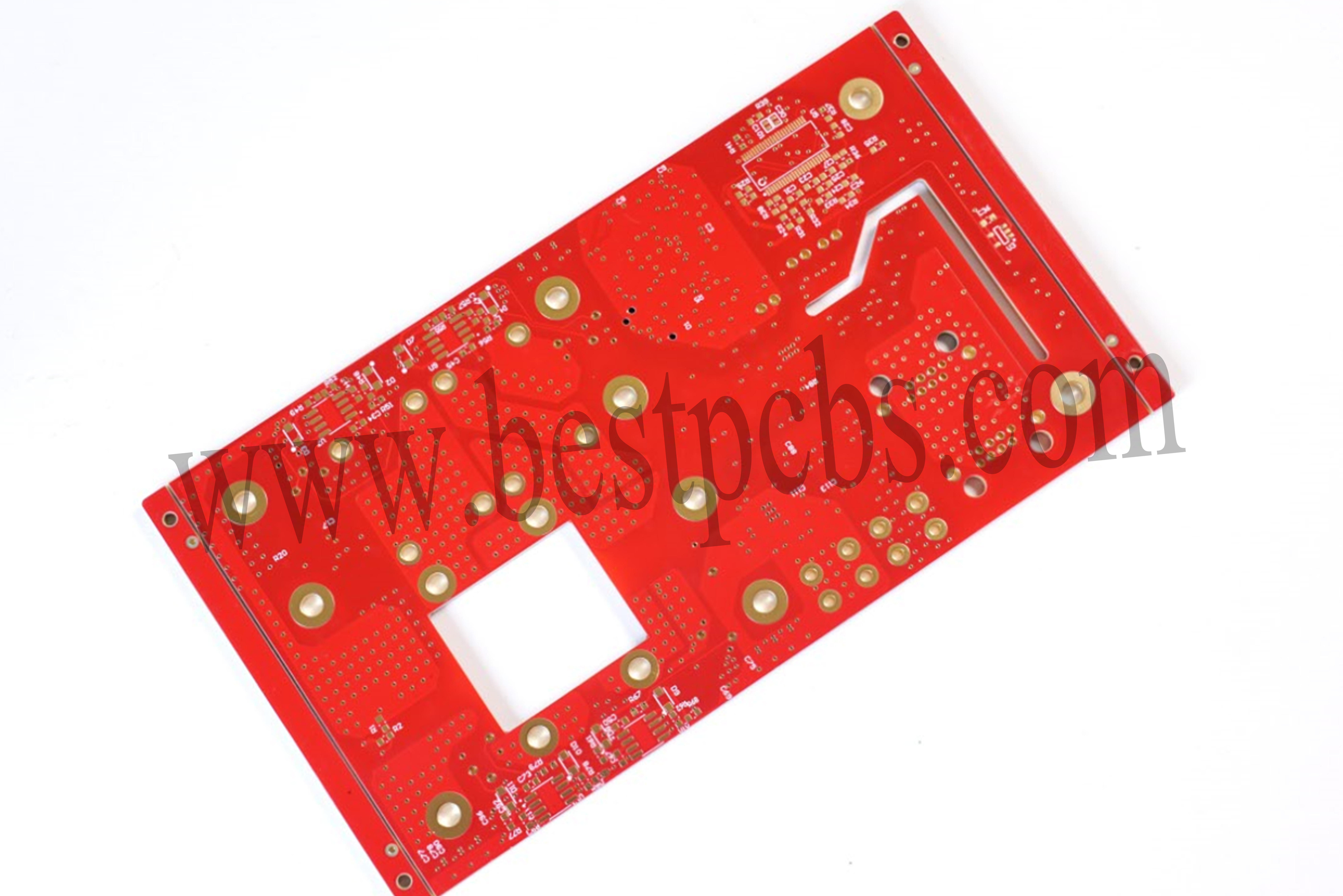
Single Sided 6 Layer IMS Board Design Requirements
| Parameter Category | Design Requirement Specifications |
| Substrate Structure | Single-sided routing (top layer only), 6-layer insulated metal substrate (aluminum or copper base), ensuring efficient heat dissipation path |
| Substrate Thickness | Metal substrate thickness: 1.0–3.0mm (recommended 1.5mm); total board thickness: 0.6–6.0mm (including dielectric layers and copper foil), adaptable to varying thermal management needs |
| Dielectric Layer Thermal Conductivity | Multiple tiers available: 0.5–8.0 W/m·K (standard options: 1.0/2.0/3.0/5.0/8.0 W/m·K), meeting high-power device thermal management requirements |
| Copper Foil Thickness | Range: 0.5–6.0 oz (commonly 1–4 oz), supporting different current carrying and signal transmission requirements |
| Minimum Line Width/Spacing | Standard process: 0.2mm line width / 0.225mm spacing; high-precision process: 0.075mm line width / 0.075mm spacing (requires special process support), enabling precise routing |
| Impedance Control | Single-ended impedance: 50Ω/55Ω (4–5mil line width); differential impedance: 90Ω/100Ω (4–5mil line width / 8–12mil spacing), ensuring signal integrity |
| Layer Stack-up | Recommended symmetric structure: Top-GND-PWR-SIG-GND-Bottom, reducing PCB warpage risk and enhancing mechanical stability |
| Surface Finish | Options: HASL, ENIG, OSP, immersion silver; solder mask colors: white/black/yellow selectable, accommodating diverse application scenarios |
| Voltage Withstand | Dielectric layer voltage resistance > 3kV (AC/DC), ensuring electrical safety in high-voltage environments |
| Drilling Accuracy | Standard mechanical drilling: minimum hole size 0.4mm; advanced process: minimum hole size 0.3mm, meeting high-density interconnection demands |
Single Sided 6 Layer IMS Design Guideline
A design guide about single sided 6 layer IMS:
1. Stackup Structure Design
- Standard Architecture: Utilize “Top Layer (Signal Layer) – GND02 (Ground Plane) – S03 (Signal Layer) – PWR04 (Power Plane) – GND05 (Ground Plane) – BOTTOM (Metal Substrate)” stackup to ensure tight coupling between signal layers and reference planes (spacing ≤0.1mm), reducing signal return path impedance. Metal substrate (e.g., aluminum/copper) serves as bottom thermal core, with dielectric layer (e.g., alumina/boron nitride filled) thickness controlled at 0.1-0.3mm and thermal conductivity 8-12 times higher than FR4. Electromagnetic simulation confirms this structure reduces high-frequency crosstalk below -30dB, meeting 5G RF module EMC requirements.
- Optimization Scheme: For high-density designs, adopt “Top-GND-S03-S04-PWR-BOTTOM” configuration while avoiding direct coupling between adjacent signal layers through ground plane isolation. Inserting 0.5mm FR4 isolation layers in high-speed digital circuits reduces inter-layer capacitance by 40% while maintaining impedance continuity.
2. Material Selection and Dielectric Properties
- Substrate Materials: Prioritize IPC-4101 compliant low-Dk (≤4.5) and low-Df (≤0.01) materials (e.g., Rogers 4350, Panasonic Megtron 6) for stable high-frequency signal transmission. Metal substrates undergo CTE matching tests to prevent delamination from soldering stress. Aluminum substrate CTE (22ppm/℃) maintains 30% compatibility with FR4 (14ppm/℃) to prevent solder joint fatigue.
- Dielectric Layer: Ceramic-filled prepregs (e.g., Bergquist Thermal Clad) withstand ≥260℃ for lead-free soldering. Thermal conductivity ≥2W/m·K ensures efficient heat transfer to metal substrate. In LED applications, this material reduces thermal resistance to 0.8℃/W, tripling heat dissipation efficiency versus FR4.
3. Thermal Management Optimization
- Thermal Strategies: Deploy thermal vias (diameter ≥0.3mm, pitch ≤1.5mm) beneath power devices to form heat channels to metal substrate. Top/bottom copper pour coverage ≥70% with 1oz copper thickness for enhanced thermal conductivity. Bare copper design (no solder mask) in high-power areas reduces thermal resistance to 0.5℃/W. Thermocouple measurements show 20% improvement in IGBT temperature uniformity.
- Thermal Simulation: ANSYS Icepak/Flotherm simulations ensure junction temperature ≤105℃. Case studies show IMS reduces temperatures by 50-70℃ versus FR4 (e.g., LED module from 129℃ to 62℃). Electric vehicle controllers achieve >100k-hour power module lifespan, meeting automotive reliability standards.
4. Signal Integrity and EMI Control
- Impedance Control: High-speed differential pairs (USB3.0, PCIe) require 100Ω±10% impedance matched via Polar SI9000 calculations. Single-ended traces maintain 50Ω impedance to minimize reflections. At 10GHz, this matching limits insertion loss to <2dB and improves eye diagram opening by 15%.
- Routing Rules: Critical signals (e.g., clocks) route in inner layers away from power planes. Adjacent layers use perpendicular routing directions with ≥3x line width spacing. 45° via transitions reduce signal reflections. DDR4 routing follows 3W rule (spacing ≥3x line width) to limit crosstalk noise <5% per JEDEC standards.
- EMI Mitigation: Ground fences surround sensitive signals with via spacing ≤λ/20 (λ = operating wavelength). Stitching vias connect power and ground planes to form low-impedance return paths. RF modules achieve FCC Class B radiation compliance through CISPR 32 certification.
5. Design for Manufacturing (DFM)
- Manufacturing Specs: IPC-6012 Class 3 compliant with minimum trace/space ≥3mil (0.076mm) and via diameter ≥0.2mm. BGA pads use non-SMD design with 0.1mm solder mask expansion. 01005 component placement achieves 99.9% yield via AOI inspection.
- Component Placement: Polarized components align uniformly to prevent automated assembly errors. SMD components avoid board edges (5mm clearance) to prevent splitting damage. Power components (inductors) use thermal pads with ≥4 thermal vias to ground plane. Server motherboard layouts reduce thermal gradients to 5℃/cm.
- Testing Validation: Gerber files include stackup details, impedance profiles, and drill charts. AOI/flying probe tests ensure <100ppm defect rates. X-ray inspection confirms >95% via fill per IPC-A-610 standards.
6. Advanced Processes and Surface Finishes
- Surface Treatments: ENIG or OSP finishes comply with RoHS/REACH. Metal substrates receive anodization for corrosion resistance. Marine applications achieve >1000-hour salt spray resistance per MIL-STD-883.
- HDI Technologies: Blind/buried vias (e.g., 1-3 layers) via HDI processes reduce inter-layer signal loss. Backdrilling removes via stubs to improve signal integrity. Millimeter-wave radar modules achieve 3dB loss reduction, meeting 802.11ad requirements.
7. Industry Standards and Certifications
- Standard Adherence: IPC-2221 (design), IPC-A-600 (appearance), IPC-4101 (materials) compliance. Automotive/medical applications require AEC-Q200 or IEC 60601-1 certification. Medical implants follow ISO 13485 for FDA 21 CFR Part 820 compliance.
- Certification Process: ISO 9001/ISO 14001 certifications ensure process control and environmental compliance. Critical products obtain UL V-0 flammability and TÜV safety certifications. Consumer electronics certifications accelerate market entry and reduce time-to-market.
8. Reliability Testing and Validation
- Thermal Cycling: -40℃~125℃ cycling for 1000 cycles validates solder joint reliability. CAF testing confirms dielectric moisture resistance. Aerospace modules simulate extreme thermal environments for vacuum reliability validation.
- Signal Testing: TDR verifies impedance matching, oscilloscopes measure eye diagrams, and S-parameters confirm <2dB insertion loss at 10GHz. 5G base stations achieve >20dB SNR per 3GPP standards.
How to Make A Single Sided 6 Layer IMS?
Below are production process for single sided 6 Layer IMS board:
1. Base Material Preparation and Pretreatment
- Select high-thermal-conductivity metal substrates (e.g., aluminum or copper) with thickness typically 1.5–3mm. Surface treatment includes polishing and cleaning to remove oil and oxide layers, ensuring strong adhesion to the insulating layer.
- The insulating layer uses high-thermal-conductivity materials (e.g., polyimide, epoxy resin filled with ceramic powder or alumina) with thickness controlled at 50–200μm based on thermal design requirements. Copper foil thickness (e.g., 35–70μm) is chosen according to circuit needs and pre-laminated to the insulating layer.
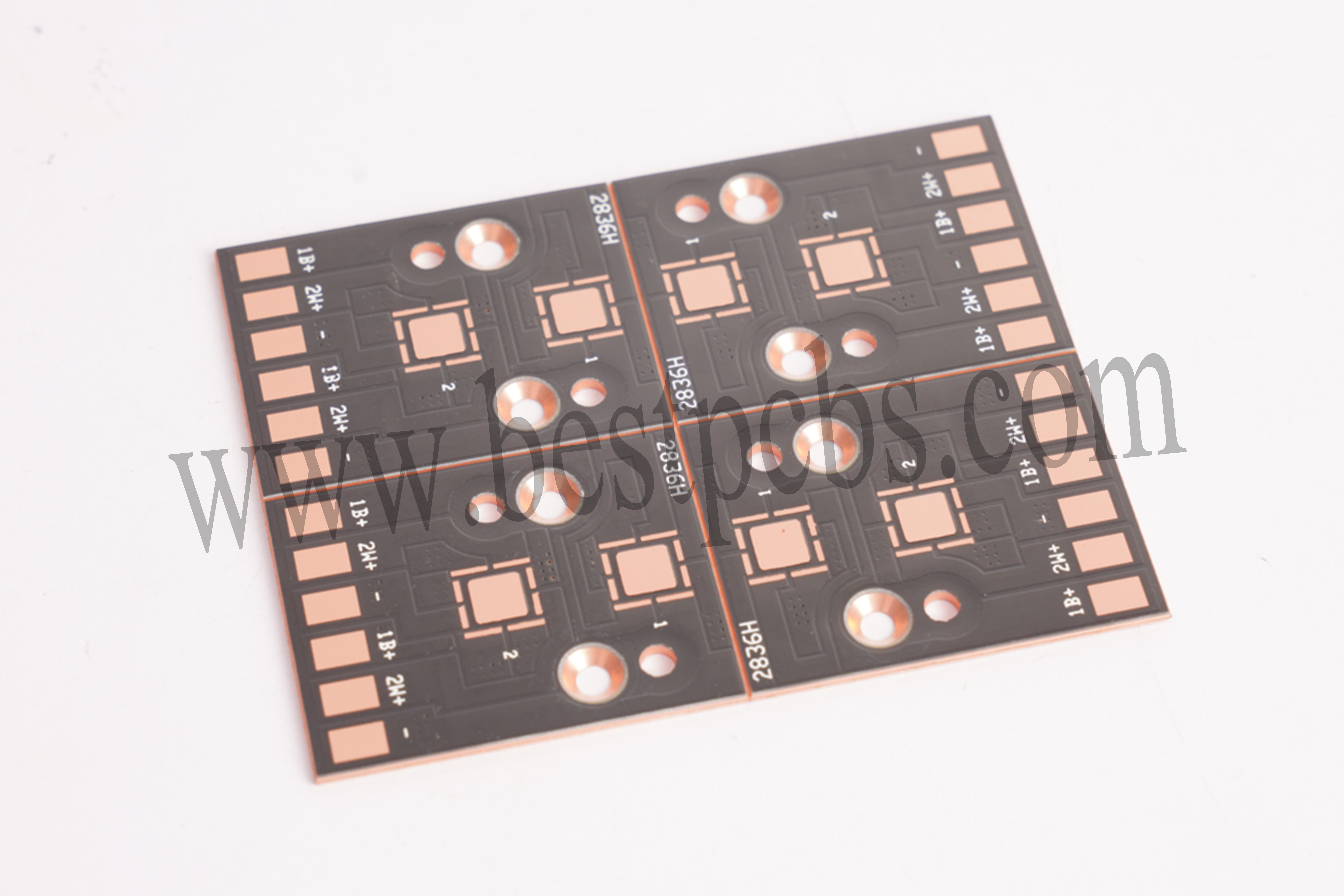
2. Inner Layer Circuit Pattern Transfer
- For inner layers (L2–L5): After substrate cutting, perform cleaning (alkaline degreaser at 40°C ultrasonic cleaning for 5 minutes), dry film application (35μm thickness), UV exposure (80–100mJ/cm²), development (1% sodium carbonate solution at 30°C), and etching (acidic copper chloride etching solution with Cu²⁺ concentration 180–220g/L) to form circuit patterns.
- Each layer undergoes AOI inspection to ensure line width deviation ≤±0.02mm and no short/open circuit defects.
3. Lamination and Structural Forming
- Use a stack-up configuration of “outer layer substrates (L1, L6) – prepreg (PP) – inner layer substrates (L2–L5) – PP”. PP thickness is 0.1–0.2mm (e.g., 2116/7628 type). Alignment is ensured via positioning pins with deviation ≤±0.05mm.
- Lamination controls heating rate (2°C/min to 120°C, then 1°C/min to 180°C), pressure (5–30kg/cm²), and curing time (60 minutes at 180°C) to achieve interlayer bonding strength ≥1.0N/mm and warpage ≤0.1%.
4. Drilling and Hole Metallization
- Drilling employs CCD visual positioning (accuracy ±0.01mm) with carbide drill bits (for hole diameters 0.3–0.6mm) or diamond-coated bits (for diameters ≤0.2mm).
- Post-drilling desmearing uses alkaline potassium permanganate solution (70°C for 10–15 minutes), followed by chemical copper plating (0.5–1μm thickness) and electroplating (acidic sulfate copper plating, current density 1–1.2A/dm² for 35μm copper thickness in 30 minutes). Ensure hole wall copper thickness uniformity deviation ≤±10% and void rate ≤1%.
5. Outer Layer Circuit and Solder Mask Application
- Outer layer circuit pattern transfer follows similar steps to inner layers but includes solder mask coverage areas. Solder mask is applied via screen printing (15–20μm thickness) or spraying, followed by UV exposure (100–120mJ/cm²) and development.
- Window size deviation ≤±0.03mm. Post-curing, solder mask adhesion passes 3M tape test (≥0.8N/mm) and withstands soldering temperature of 260°C for 10 seconds without peeling.
6. Surface Finish and Final Inspection
- Surface finishes include ENIG (0.1μm gold over 2–3μm nickel), HASL (lead-free solder thickness 5–10μm), or immersion silver/tin.
- Final inspection includes full electrical testing (100% continuity coverage, impedance deviation ≤±5%), visual inspection (solder mask defects, silkscreen errors), and reliability testing (thermal cycling -40°C to 125°C for 100 cycles, vibration test 10–2000Hz/20g/100 hours).
7. Quality Control and Traceability
- Critical processes (lamination, drilling, plating) are monitored in real-time for parameters (temperature ±2°C, pressure ±1kg/cm²) with hourly data recording.
- First-article inspection for each batch passes full testing (thickness, impedance, electrical performance) before mass production. Finished products are assigned unique traceability codes, recording substrate batch, process parameters, and test data, stored for ≥3 years for fault traceability.
Why Choose EBest Circuit (Best Technology) as Single Sided 6 Layer IMS Manufacturer?
Reasons why choose us as single sided 6 layer IMS manufacturer:
19 Years of Dedicated Expertise in Metal Substrate Manufacturing:
- Since 2006, we have specialized in metal substrate and IMS circuit board production for 19 years, serving over 5,000 global clients and completing 20,000+ successful projects. Our mastery of 6-layer IMS technologies including lamination processes, blind/buried via techniques, and surface treatments enables precise solutions to common industry challenges like warpage and signal interference, earning international recognition for technical maturity.
Complimentary DFM Design Optimization to Minimize Development Risks
- We offer end-to-end free DFM (Design for Manufacturability) services, intervening early in the design phase to analyze circuit layout, impedance matching, and thermal design using professional simulation tools. This proactive approach reduces production risks, with clients achieving 40% shorter development cycles and 30% lower trial costs on average over the past three years.
Stringent Quality Control System with Full Traceability
- Adhering to ISO 9001 standards, our 18-step inspection process employs AOI optical detection and X-RAY scanning to ensure full compliance with IPC-6012 requirements. With a yield rate exceeding 99.2% and a repeat customer rate of 85% in recent years, our quality reliability is backed by measurable performance data.
Transparent Pricing with Competitive Cost-Performance Ratio
- Leveraging in-house manufacturing and scale advantages, we eliminate middleman markups to offer prices 10-15% below industry averages. Our tiered pricing model ensures cost efficiency for high-volume orders without compromising quality, delivering premium 6-layer IMS products at fair and transparent rates.
24-Hour Rapid Prototyping for Market Advantage
- Our automated prototyping line supports 24-hour turnaround for 6-layer IMS samples. Digital process management enables full traceability from design confirmation to sample dispatch, ensuring swift responses for urgent projects and accelerating time-to-market for competitive edge.
Flexible Small-Batch Customization for Diverse Needs
- We accommodate small-batch orders starting from 50 pieces, ideal for startups and R&D validation. Through modular production lines and flexible processes, we maintain efficiency from single-unit prototypes to mass production, supporting full lifecycle needs from prototyping to volume manufacturing.
Fast and Reliable Delivery with Guaranteed Timeliness
- Standard orders ship within 7-10 working days, with expedited options available in 3-5 days. Our end-to-end process control achieves a 98% on-time delivery rate surpassing industry benchmarks bto eliminate concerns over lead times and ensure smooth project progression.
One-Stop Service for Integration
- From design consultation and material selection to manufacturing and logistics, our professional team provides comprehensive one-stop solutions. This streamlines technical, cost, and scheduling challenges, allowing clients to focus on core innovations while we handle the rest with precision.
Global Client Success Stories and Proven Performance
- Our portfolio includes collaborations with leading global firms across 5G communications, industrial control, and automotive sectors. Client feedback consistently highlights exceptional performance in thermal management, reliability, and cost-effectiveness, with growing repeat business and referral rates underscoring the tangible value of our solutions.
Our Copper IMS PCB Manufacturing Capabilities
| Base material: | Copper/Aluminum Alloy |
| Thermal Conductivity (dielectric layer): | 0.8, 1.0, 1.5, 2.0, 3.0 W/m.K. |
| Board Thickness: | 0.5mm~3.0mm(0.02″~0.12″) |
| Copper thickness: | 0.5 OZ, 1.0 OZ, 2.0 OZ, 3.0 OZ, up to 10 OZ |
| Outline: | Routing, punching, V-Cut |
| Soldermask: | White/Black/Blue/Green/Red Oil |
| Legend/Silkscreen Color: | Black/White |
| Surface finishing: | Immersion Gold, HASL, OSP |
| Max Panel size: | 600*500mm (23.62″*19.68″) |
| Packing: | Vacuum/Plastic bag |
| Samples L/T: | 4~6 Days |
| MP L/T: | 5~7 Days |
How to Get A Quote For Your IMS PCB Project?
Below is a Material List for IMS Project Quotation:
Technical Documents:
- Gerber files, drilling files, PCB engineering drawings, circuit design (including 6-layer structure, substrate material such as FR4, surface finish such as ENIG, impedance control requirements).
- Bill of Materials (BOM) listing component names, models, quantities, suppliers, and specifications.
Process Parameters:
- Minimum trace width/spacing, special processes (e.g., blind/buried vias), surface finish methods, solder mask color.
- Stack-up diagram, board thickness (0.6-3.0mm), ink color.
Quantity and Delivery
- Production quantity, delivery date, packaging requirements.
- Testing standards (e.g., RoHS certification, environmental compliance).
Corporate Qualifications
- Business license, industry certifications (e.g., ISO), past project references.
- Legal representative authorization letter, credit report (no discreditable records).
Quotation Details
- Unit price, total price, taxes, payment terms.
- Special interface/software configurations (e.g., IMS system integration needs).
Additional Documents
- Sample test reports, third-party audit reports (cost verification).
- Draft contract, after-sales service clauses.
Welcome to contact us if you have any request for IMS PCB: sales@bestpcbs.com.