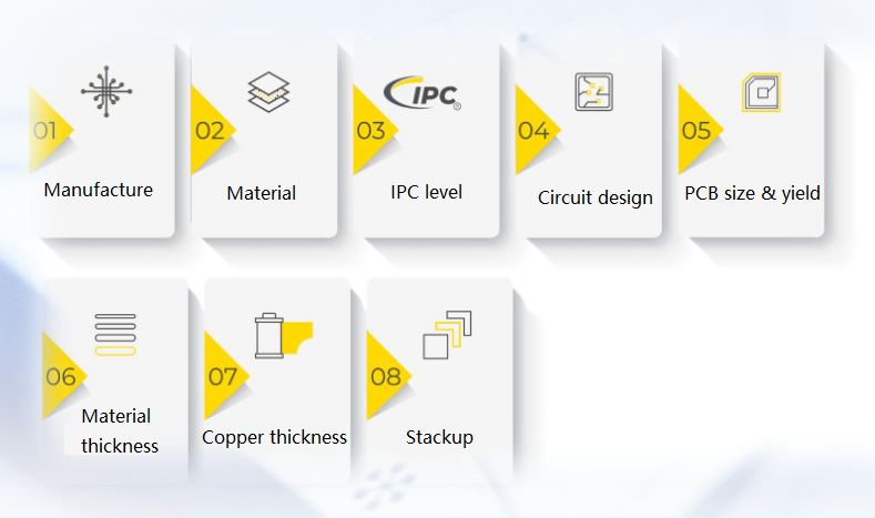
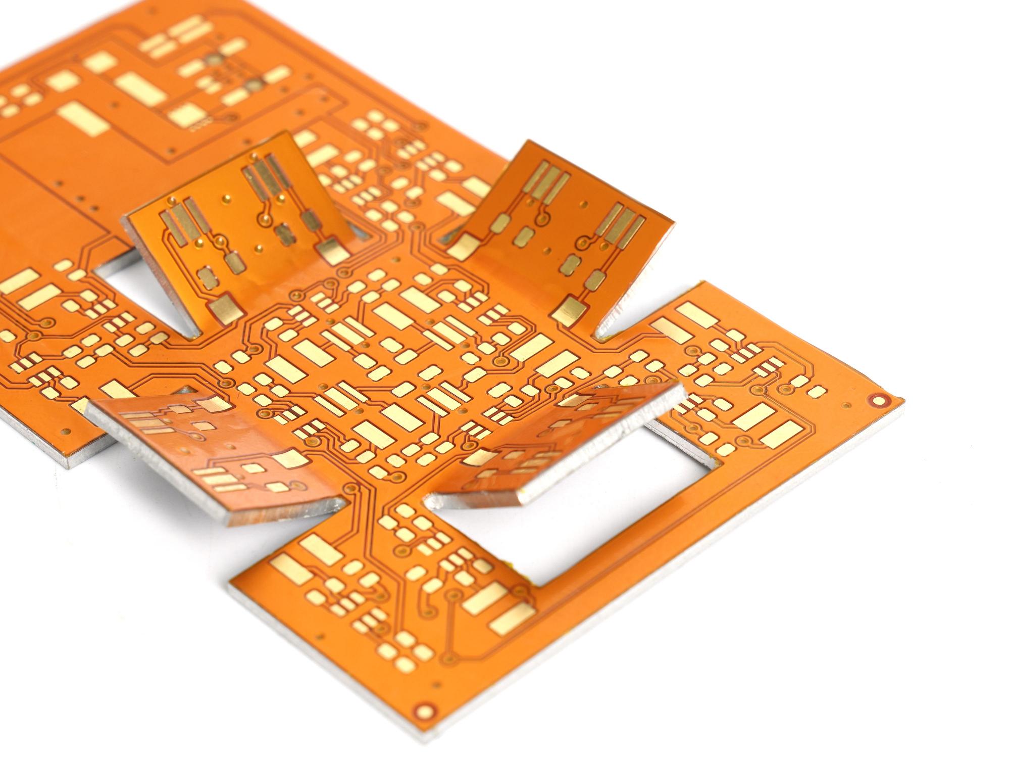
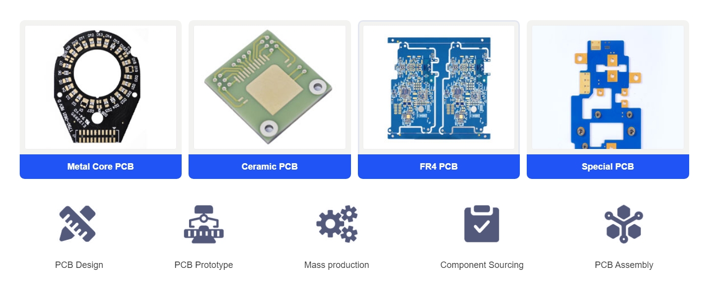
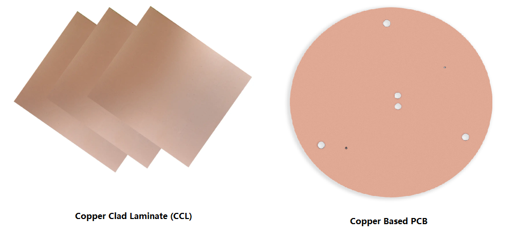
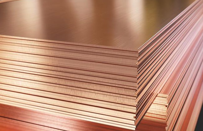
What is Copper Clad Laminate?
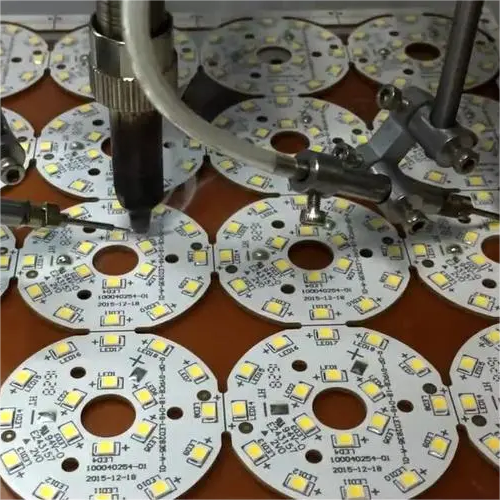
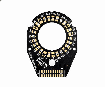
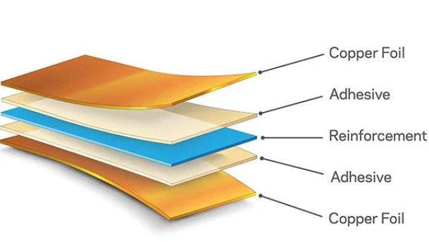
Copper clad laminate short for CCL, it is a foundational material in the electronics industry. It consists of a thin copper foil bonded to one or both sides of a non-conductive substrate like fiberglass or resin. This combination creates a durable and conductive material that serves as the base for creating printed circuit boards (PCBs). The copper layer facilitates the transmission of electrical signals, while the insulating substrate supports the board’s structural integrity.
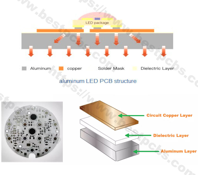
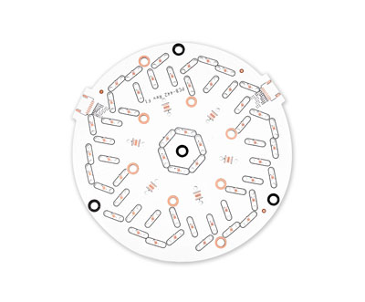
CCL comes in various thicknesses and types, depending on the application. It’s a critical part of most electronic devices, from smartphones to industrial machines. Its main role is to support the etching of circuit patterns, where unnecessary copper is removed, leaving conductive paths that enable electrical connections. Below is a structure of a double sided copper clad laminate:
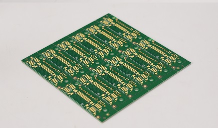
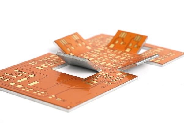
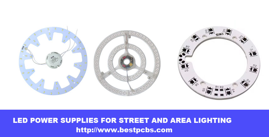
What is Copper Clad Board Used For?
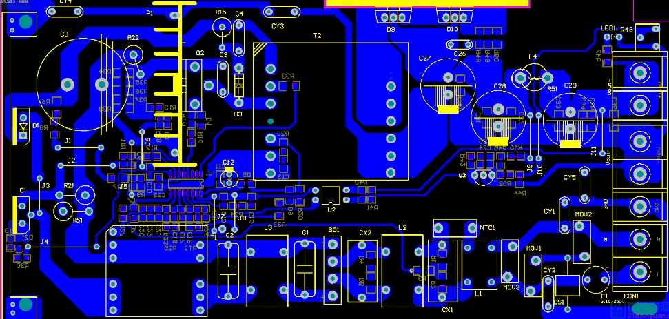
Copper clad boards are widely used in PCB manufacturing. Their role is to provide a surface for electrical components to connect through conductive copper traces. CCLs are widely used in applications including, but not limited to:
- Electronic products: Copper clad board is the basic material of electronic products, used to manufacture various electronic equipment circuit board, such as TV, radio, computer, computer and so on.
- Communication equipment: Mobile phones, tablet computers, routers and other communication equipment a large number of copper clad laminate.
- Computers and peripherals: Computer motherboards, graphics cards, hard disks, etc., need a large number of copper-clad boards.
- Automotive electronics: Electronic equipment in modern automobiles, such as ABS, air conditioning, navigation, etc., need to use copper clad board.
- Military: Electronic components in military equipment also need to use a large number of copper-clad boards.
In addition, copper clad boards are also used in industrial control, medical instruments, national defense, aerospace and other fields. With the development of technology and the increase of application demand, the use of copper clad plate in electronic products is more and more extensive, which plays an important role in promoting the renewal of social production and living tools. For example, the development of the Internet of Things and artificial intelligence, as well as the application of 5G communication technology, have greatly increased the demand for copper clad sheets.
What is the Market Report for Copper Clad Laminate?
The market for copper clad laminate has grown steadily due to the increasing demand for consumer electronics, automotive advancements, and telecommunication developments. The global CCL market is expected to expand significantly over the next few years, driven by technological advancements in 5G, renewable energy systems, and electric vehicles.
Key players in this market are working to develop lighter, thinner, and more efficient CCLs to keep pace with the growing need for high-performance electronics. Manufacturers exploring new materials and production methods to reduce costs while enhancing performance. The future looks promising, with a forecast of rapid growth driven by the electronics industry’s evolution.
Is Copper Clad Better Than Copper?
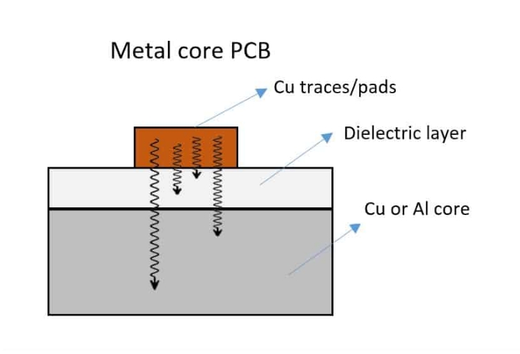
Copper clad laminate is a more practical option for PCBs than solid copper because it provides the required conductive properties at a lower cost. While copper is an excellent conductor, using copper as metal core PCBs would be expensive and impractical. CCL offers the same conductivity benefits but adds a lightweight, non-conductive layer that provides structural support.
Electrical Conductivity and Cost Efficiency
While pure copper has excellent electrical conductivity, copper clad laminates (CCLs) provide a balance between cost and performance. In a copper clad board, only a thin copper layer is used, which significantly reduces the amount of copper needed compared to using solid copper. For applications like PCBs, where large surfaces need copper conductivity but do not require the full thickness of copper, copper clad is more efficient and economical.
Thermal Management
Copper clad materials often have better thermal management properties due to the substrate’s ability to dissipate heat while maintaining the copper layer’s high conductivity. Pure copper, while an excellent heat conductor, may not offer the same level of thermal dissipation when used alone in complex electronic assemblies. For instance, in multi-layer PCBs, copper clad boards help balance the need for heat management and conductivity by using the copper layer efficiently while the base material manages thermal stress.
Structural Support and Durability
Copper clad laminates provide added structural support compared to pure copper sheets. The non-conductive substrate, often made of fiberglass, resin, or other materials, adds durability and rigidity to the thin copper layer. By contrast, is soft and flexible, making it unsuitable for structural applications without some form of backing material.
Corrosion Resistance
Copper, though highly conductive, is prone to oxidation and corrosion over time, which can affect its performance in certain environments. Copper clad laminates, however, are often treated with protective coatings or layered with other materials to enhance their resistance to corrosion.
Weight Considerations
Another important factor is weight. Copper is a dense metal, and using thick copper layers can significantly increase the weight of a product. In contrast, copper clad laminates achieve high conductivity with only a fraction of the copper’s weight.
How Thick is Copper Clad Board?
The thickness of a copper clad board depends on its intended application. Standard copper thicknesses for CCL are measured in ounces per square foot, typically ranging from 0.5 oz to 2 oz per square foot. This translates to about 17 to 70 microns. For high-power applications, thicker copper, such as 3 oz or more, may be used.
On the other hand, the thickness of the laminate itself can also vary, depending on whether it’s a single-layer, double-layer, or multilayer board. The insulating substrate can range from 0.2 mm to several millimeters, depending on the application. The total thickness of the copper clad board is a combination of the copper foil and the insulating material.
How Much Does Copper Cladding Weigh?
The weight of copper cladding is typically expressed in ounces per square foot. A common weight is 1 oz of copper, which means that a square foot of copper clad board has a 1-ounce copper layer. This is approximately 35 microns thick. Heavier copper cladding, such as 2 oz or 3 oz, is also used for applications that require higher current-carrying capacity or greater durability.
It’s important to balance the weight with the application needs. Higher copper weight provides better conductivity and durability but adds cost and weight to the final product. Therefore, the choice of copper weight in CCL depends largely on the required performance and cost considerations.
Copper Clad Laminate Price
The price of copper clad laminate varies based on several factors such as copper thickness, substrate material, board size, and production volume. Standard-grade CCL is more affordable, while high-end options with specialty substrates like Teflon or ceramic tend to be more expensive.
On average, copper clad laminate costs range from $5 to $15 per square meter for common types. However, high-performance laminates designed for demanding environments, such as those used in aerospace or military applications, can be significantly more expensive.
Global market trends, material shortages, and the demand for electronics heavily influence pricing. Recently, fluctuations in copper prices and supply chain disruptions have impacted the cost of CCL. Still, bulk orders or long-term contracts with suppliers can help reduce costs for large manufacturers.
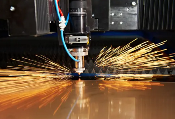
How to Cut Copper Clad Laminate?
CCL requires careful handling to ensure precise cuts without damaging the copper layer or the substrate. The cutting method will vary depending on the thickness and material, but overall, clean and accurate techniques are key.
1. Choose the Right Tools
The tools you use depend on the thickness of the copper clad laminate. Thin CCL can be cut with a utility knife, while thicker boards require specialized tools like a PCB shear or laser cutter.
2. Prepare the Work Area
Before cutting, ensure that your workspace is clean and stable. Use a flat surface to keep the laminate steady during cutting. For larger boards, use clamps to secure them in place. Always wear protective gear like goggles and a mask, especially when working with power tools to avoid dust and debris.
3. Measure and Mark the Cutting Line
Accurate measurements are crucial for a clean cut. Use a ruler or measuring tape to mark the cutting line and draw it clearly with a permanent marker. Double-check your measurements to avoid mistakes before cutting.
4. Score the Copper Clad Laminate
For thin laminates, use a utility knife to score along the marked line. Score the copper side first, then flip it over and score the substrate. Once both sides are scored, gently bend the laminate along the line until it snaps cleanly.
5. Cut Thick Copper Clad Laminate
For thicker CCL, use a guillotine PCB shear or a Dremel tool. A PCB shear provides a clean, straight cut, while a Dremel is useful for cutting complex shapes. For high precision, a laser cutter is the best choice, especially for intricate designs.
6. Deburr and Smooth the Edges
After cutting, the edges may be rough. Use a file to smooth out any jagged areas, then finish with fine-grit sandpaper.
Safety is important when cutting CCL. Fiberglass and other substrate materials can produce harmful dust. Always wear a dust mask and safety goggles, and work in a well-ventilated area to minimize exposure to particles. In addition to this, avoid over-scoring the laminate, which can damage the substrate or cause copper peeling. Make sure to apply consistent pressure while cutting to prevent uneven edges. Always prioritize safety by using proper protective gear to avoid injuries.
Copper Clad Laminate Suppliers
Numerous suppliers provide copper clad laminate globally. The selection of a supplier depends on factors like the type of laminate, application requirements, and volume needed. Some well-known suppliers include:
- Kingboard Laminates
- Panasonic
- Isola Group
- Nan Ya Plastics
- Shengyi Technology
- Rogers Corporation
- Ventec International Group
- Doosan Corporation
- Iteq Corporation
- Mitsubishi Gas Chemical
With over a decade of effort and experience, EBest Circuit (Best Technology) has been actively contributing to the growth of this business. Certified with ISO9001, ISO13485, IATF16949, UL, and RoHS, the company is fully capable of delivering high-quality, eco-friendly PCBs and various types of copper clad laminates at competitive prices.