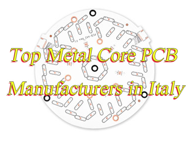
Looking for Australia PCB manufacturer? This blog is mainly about list and selection guide, evaluation methods of production capability, lead time for Australia PCB manufacturer.
For PCB designers perfecting new circuit diagrams, engineers resolving production bottlenecks, or procurement teams ensuring a stable supply, finding a trustworthy global PCB manufacturer is not just a choice, but a crucial decision for the success of their projects.
This is why a reliable global PCB manufacturer is so important. As a leader in global PCB solutions, EBest Circuit (Best Technology) has specialized in PCB prototyping, custom PCB design, and mass production for 19 years. Our experienced team of engineers provides free engineering services and DFM (Design for Manufacturability) checks to ensure the smooth production of your PCB projects. Whether you are manufacturing medical devices or industrial control systems, we can transform your excellent designs into high-quality PCB products. Contact us now if you need any help for PCB design, prototyping, mass production or PCBA service: sales@bestpcbs.com.
Are You Facing These Challenges?
- You’re waiting 4+ weeks for overseas PCB prototypes, pushing your product launch past deadlines.
- Your PCB design works on paper but fails in production—no local engineer to fix it before manufacturing.
- Mass-produced PCBs have inconsistent quality, leading to rework costs that eat into your budget.
- Overseas suppliers give vague lead times, leaving you stuck when critical orders hit customs delays.
- Complex projects (medical/defense) lack the compliance support and traceability you need.
- You’ re paying hidden fees (shipping, customs, duties) on “low-cost” overseas quotes, total costs spiral.
End-to-End Support from Requirement to Delivery
- Requirement & Design: Share your Gerber files or even a rough sketch, and we’ll run a free Design for Manufacturability (DFM) audit—no strings attached. This isn’t just a quick check: we flag hidden flaws like overly narrow traces, thermal hotspots, or impedance mismatches that often slip past overseas suppliers. You’ll get a clear report with revised files if needed, so your design doesn’t fail in production and force costly reworks. We also lock in a fixed, all-inclusive quote upfront—no surprise fees later.
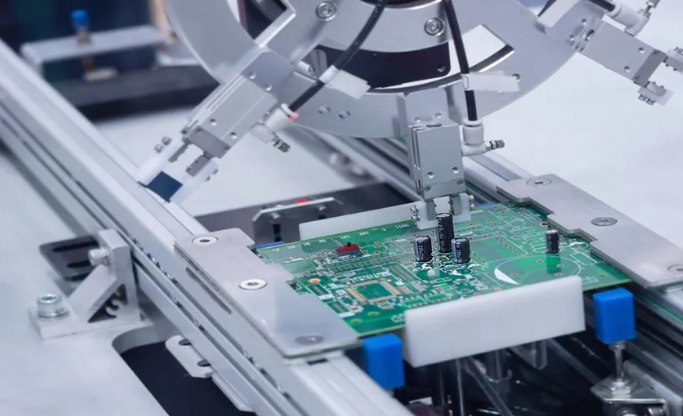
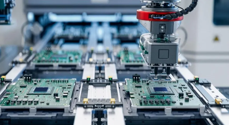
- Prototyping & Production: Tired of 4+ week waits for overseas prototypes? Our standard prototypes ship in 1–5 days, with 24–48 hour expedited options for tight deadlines. We keep FR-4, Rogers, and Polyimide in stock, so material shortages never slow you down. For mass production, our Sydney facility uses automated CNC drilling and AI-powered optical inspection (AOI) to avoid the inconsistent quality that plagues budget overseas shops. Every batch comes with real-time test data, so you know exactly what you’re getting before it ships.
- Delivery & After-Sales: 80% local material sourcing means no customs delays or stuck shipments. You can track orders online 24/7, with automatic alerts for every milestone—from design approval to shipping. Each PCB includes a full traceability report, so you have clarity on material lots and test results. Even after delivery, we’re here: if you hit snags during assembly, our team provides free troubleshooting. And if we miss a committed lead time (our fault), you get 10% off your next order—no arguments, just accountability.
Why Choose EBest Circuit (Best Technology) for Global PCB Manufacturer?
Reasons why choose EBest Circuit (Best Technology) for global PCB manufacturer:
- Regulatory Certification Portfolio: Holds globally recognized certifications (ISO 9001, IATF 16949, ISO 13485, RoHS) to facilitate seamless market entry in EU/Middle East markets while minimizing compliance-related risks for buyers.
- Cost-Effective Pricing Strategy: Provides budget-conscious design alternatives via material efficiency upgrades and manufacturing process refinements, achieving 15-20% BOM cost reduction under IPC-6012 compliance, catering to cost-aware consumer electronics development.
- 24-Hour Express Prototyping: Supports urgent prototype needs with 24-hour sample delivery featuring TDR impedance checks and AOI defect detection, enabling designers to validate concepts faster and reduce time-to-market by 30%+.
- Punctual Delivery Performance: Maintains 99.2% delivery reliability through intelligent production planning and cross-regional logistics coordination, guaranteeing 12-14 day standard cycles and 7-day express options for stable procurement operations.
- High-Yield Mass Production Framework: Implements comprehensive full-lot inspection during volume manufacturing via flying probe testing and accelerated reliability stress tests, achieving sustained 98%+ yield rates to ensure flawless product delivery to engineering teams.
- Decades-Long Technical Mastery: Applies 19 years of accumulated PCB know-how through standardized workflows and failure pattern databases to rapidly pinpoint design vulnerabilities and deploy reliable engineering solutions.
- Pre-Production DFM Support: Includes complimentary manufacturing feasibility analysis in design phases, covering signal integrity modeling, impedance control guidance, and solderability enhancements to proactively address production challenges.
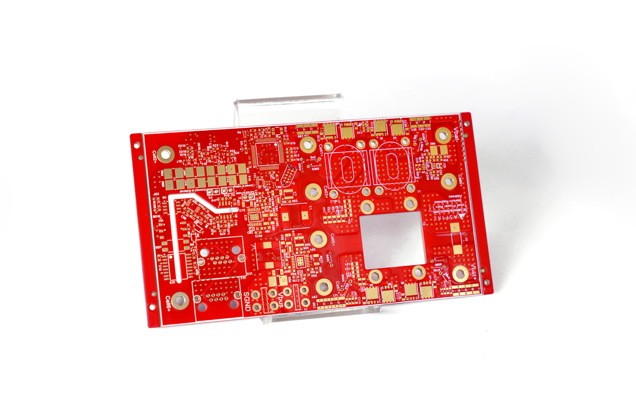
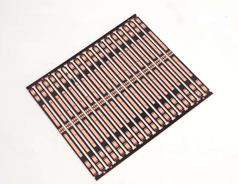
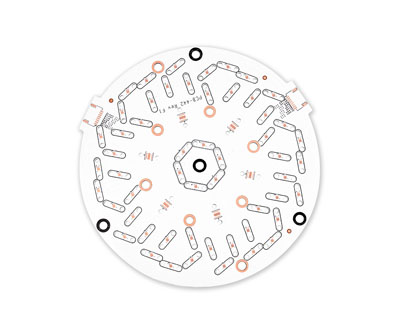
Top Australia PCB Manufacturer List
1. Allegro Services
- Main Business: Multilayer PCB manufacturing, SMD assembly, turnkey electronics solutions.
- Core Advantage: AS9100D certified, trusted by Boeing Australia for aerospace/defense projects.
- Lead Time: Prototyping 3–7 days; mass production 10–15 days.
- Process Capability: 6–24 layer PCBs, ±5% impedance control, blind/buried vias.
2. B.E.C. Manufacturing
- Main Business: Low-to-mid volume PCBs, solder paste stencils, membrane switches.
- Core Advantage: ISO 13485 certified, specialized in medical device PCB prototype-to-production.
- Lead Time: Prototyping 1–5 days; mass production 7–10 days.
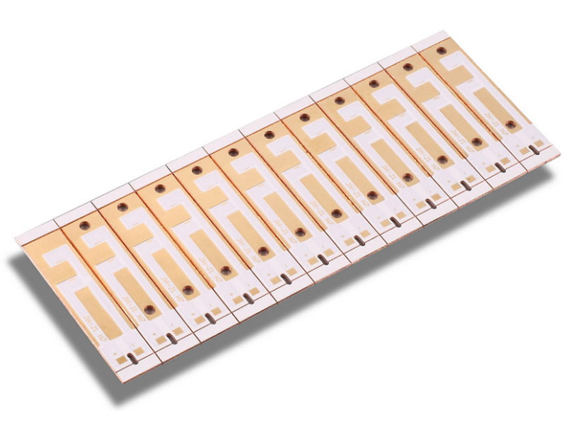
- Process Capability: 1–12 layer PCBs, FR-4/Polyimide, 0.1mm fine line.
3. Circuitwise
- Main Business: High-reliability PCBs for industrial control and automotive.
- Core Advantage: Zero-defect guarantee, on-site failure analysis lab.
- Lead Time: Prototyping 4–6 days; mass production 12–18 days.
- Process Capability: 4–32 layer PCBs, high-temperature materials (up to 260°C).
4. Elektra Printed Circuits
- Main Business: Custom PCB prototyping, small-batch manufacturing.
- Core Advantage: Free technical consultation for startups, online instant quoting.
- Lead Time: Prototyping 2–4 days; small batches 5–8 days.
- Process Capability: 1–16 layer PCBs, flexible PCBs, LED PCB arrays.
5. Entech Electronics
- Main Business: PCB assembly (PCBA), box-build integration.
- Core Advantage: DISP registered, strict component traceability for defense projects.
- Lead Time: PCBA 7–10 days; turnkey solutions 14–21 days.
- Process Capability: 2–20 layer PCBs, through-hole/SMD mixed assembly.
6. PCB Solutions Australia
- Main Business: RF and microwave PCBs for telecommunications.
- Core Advantage: Rogers/Taconic material expertise, free VSWR testing.
- Lead Time: Prototyping 5–7 days; mass production 10–14 days.
- Process Capability: 2–18 layer PCBs, high-frequency substrates (up to 40GHz).
7. RJS Electronics
- Main Business: PCBs for mining and harsh environment electronics.
- Core Advantage: IP67 conformal coating, vibration/dust resistance testing.
- Lead Time: Prototyping 6–8 days; mass production 15–20 days.
- Process Capability: 4–24 layer PCBs, ruggedized designs.
8. Tecan Australia
- Main Business: PCBs for medical and dental equipment.
- Core Advantage: ISO 13485/FDA compliant, batch-to-batch traceability.
- Lead Time: Prototyping 4–6 days; mass production 12–16 days.
- Process Capability: 2–16 layer PCBs, biocompatible materials.
How to Choose the Right Australia PCB Manufacturer?
A detailed selection guide to Australia PCB manufacturer:
1. Certifications & Compliance
- ISO Certifications: Prioritize manufacturers with ISO 9001:2015 (quality management) and ISO 13485:2016 (medical devices) for stringent quality control. AS9100D certification indicates compliance with aerospace standards.
- Regulatory Adherence: Ensure RoHS/REACH compliance for hazardous substance restrictions and environmental safety. Medical/automotive sectors require UL or SGS certifications.
2. Technical Capabilities
- Material & Layer Support: Verify compatibility with advanced materials (e.g., Rogers high-speed laminates, flexible substrates) and multi-layer capabilities (up to 20+ layers).
- Advanced Technologies: Confirm expertise in HDI (High-Density Interconnect), blind/buried vias, and rigid-flex PCBs for complex designs.
3. Production Capacity & Lead Times
- Scalability: Assess monthly/yearly capacity for prototypes (24-hour turnaround) to high-volume production (e.g., 5-day standard lead times).
- Flexibility: Ensure support for mixed batch sizes (small-run prototyping to large-scale manufacturing) and expedited options.
4. Quality Control & Testing
- Inspection Protocols: Look for in-house AOI (Automated Optical Inspection), X-ray, and flying probe testing. Statistical Process Control (SPC) ensures defect minimization.
- Validation Processes: First Article Inspection (FAI) and ongoing audits guarantee consistency. Space-grade testing (e.g., thermal cycling from -40°C to +150°C) for specialized applications.
5. Customer Service & Support
- Technical Collaboration: Dedicated engineering teams for DFM (Design for Manufacturability) feedback and pre-production consultation.
- Communication Channels: Real-time updates via online portals, responsive email/phone support, and dedicated account management.
6. Pricing & Cost Transparency
- Clear Quoting: Itemized cost breakdowns (material, labor, testing) without hidden fees. Value engineering suggestions to optimize costs.
- Payment Flexibility: Negotiable terms for long-term partnerships and bulk discounts.
7. Environmental Responsibility
- Sustainable Practices: Energy-efficient facilities, waste recycling programs (e.g., e-waste recycling to recover copper), and reduced chemical usage.
- Carbon Footprint Reduction: Energy-saving measures and partnerships with green logistics providers.
8. Industry Experience & Case Studies
- Sector-Specific Expertise: Portfolio showcasing projects in medical, automotive, aerospace, IoT, and mining. Client testimonials from Fortune 500 companies.
- Awards & Recognitions: Industry accolades (e.g., “Top 10 Australian PCB Manufacturers”) and certifications highlighting innovation and reliability.
9. Geographic Proximity & Logistics
- Local Advantage: Proximity to Australian markets reduces shipping times (e.g., 3-day domestic delivery) and customs delays.
- Global Reach: Partnerships with reliable logistics networks for international distribution and end-to-end supply chain management.
10. Research & Development Capabilities
- Innovation Pipeline: In-house R&D teams for material science breakthroughs (e.g., high-temperature substrates) and IP protection measures.
- Collaborative Solutions: Joint development programs for emerging technologies (e.g., 5G/6G, AI-driven PCB design).
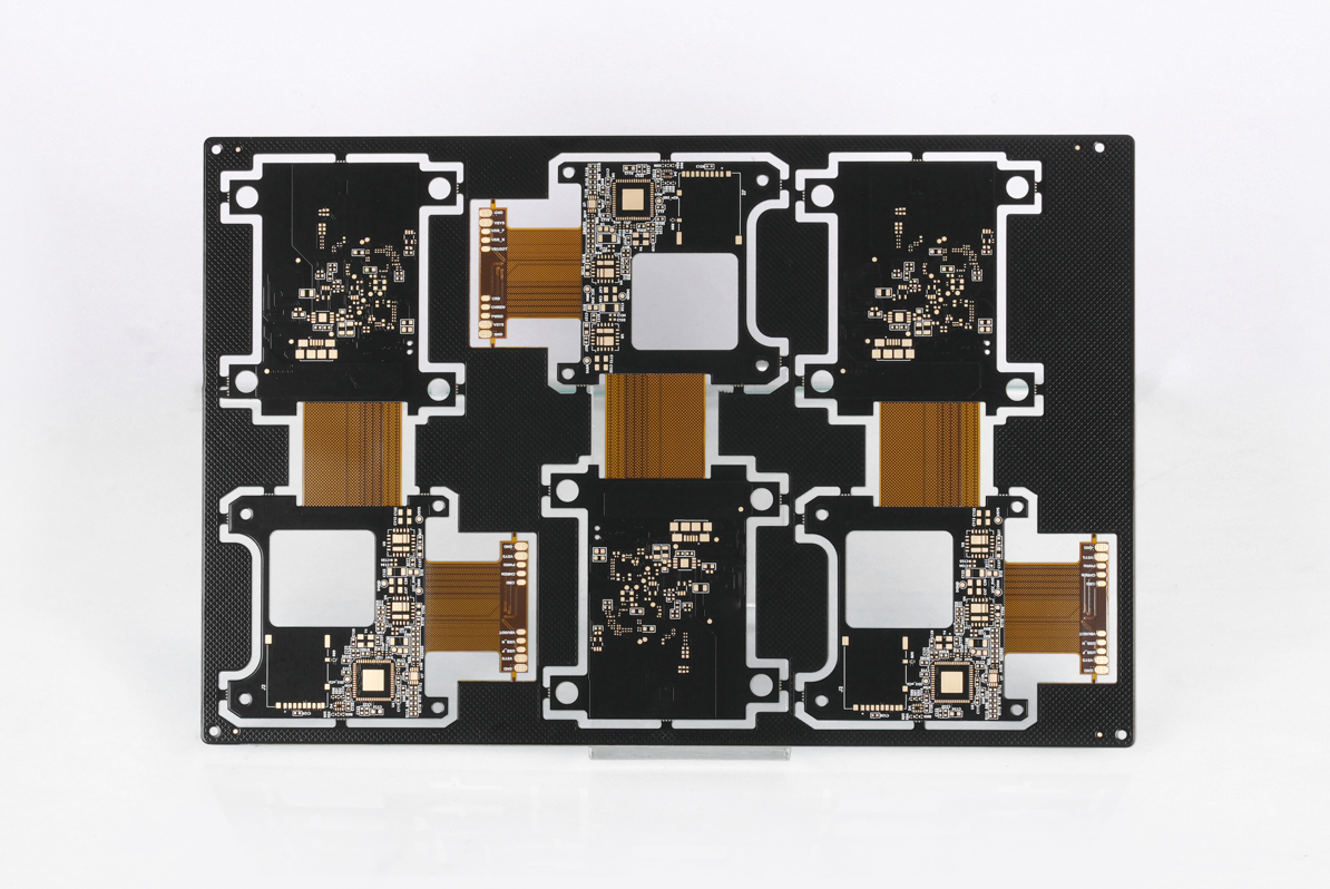
How to Evaluate an PCB Manufacturing Companies Australia’s Production Capacity?
Evaluation Methods about how to evaluate an PCB manufacturing Companies Australia‘s production capacity:
1. Production Scale & Output Metrics
- Monthly/annual PCB output volume (e.g., square feet or square meters)
- Maximum PCB size and panel capacity supported
- Production line quantity and operational hours per day
- Capacity utilization rate (target: 70%-90% for stable operations)
2. Equipment & Process Capabilities
- Advanced manufacturing equipment roster (CNC drilling machines, laser drills, automated plating lines)
- PCB layer capability (maximum layers: e.g., 32-layer multilayer boards)
- Minimum line width/space (e.g., ≤50μm for high-density requirements)
- Special process proficiency (HDI, blind/buried vias, rigid-flex, metal-core PCBs)
3. Quality & Delivery Reliability
- Quality management system certifications (ISO 9001, ISO 13485 for medical applications)
- Full-process inspection setup (raw material testing, in-line monitoring, finished product verification)
- Defect rate (DPPM) and corrective action protocols
- Lead time commitments (prototype: 24hrs-7 days; mass production: 12+ working days)
4. Supply Chain & Compliance
- Stable raw material sourcing network (certified FR4, Rogers, polyimide suppliers)
- Backup supplier arrangements for critical components
- Compliance with industry standards (RoHS, IPC, Australian defence supply chain requirements)
- Environmental compliance certifications (e.g., ISO 14001)
5. Customization & Volume Flexibility
- Ability to handle small-batch prototypes and large-scale production
- Adaptability to custom specs (impedance control, gold plating, halogen-free materials)
- Setup cost structure for repeat orders (e.g., no extra fees for volumes under 3 sq.m)
- Scalability to adjust production for order surges
6. Practical Verification Methods
- Request factory audit (equipment condition, production flow, quality control labs)
- Review past project data (similar PCB type, volume, delivery records)
- Test prototype production (assess turnaround time and process consistency)
- Check customer references for high-volume order performance
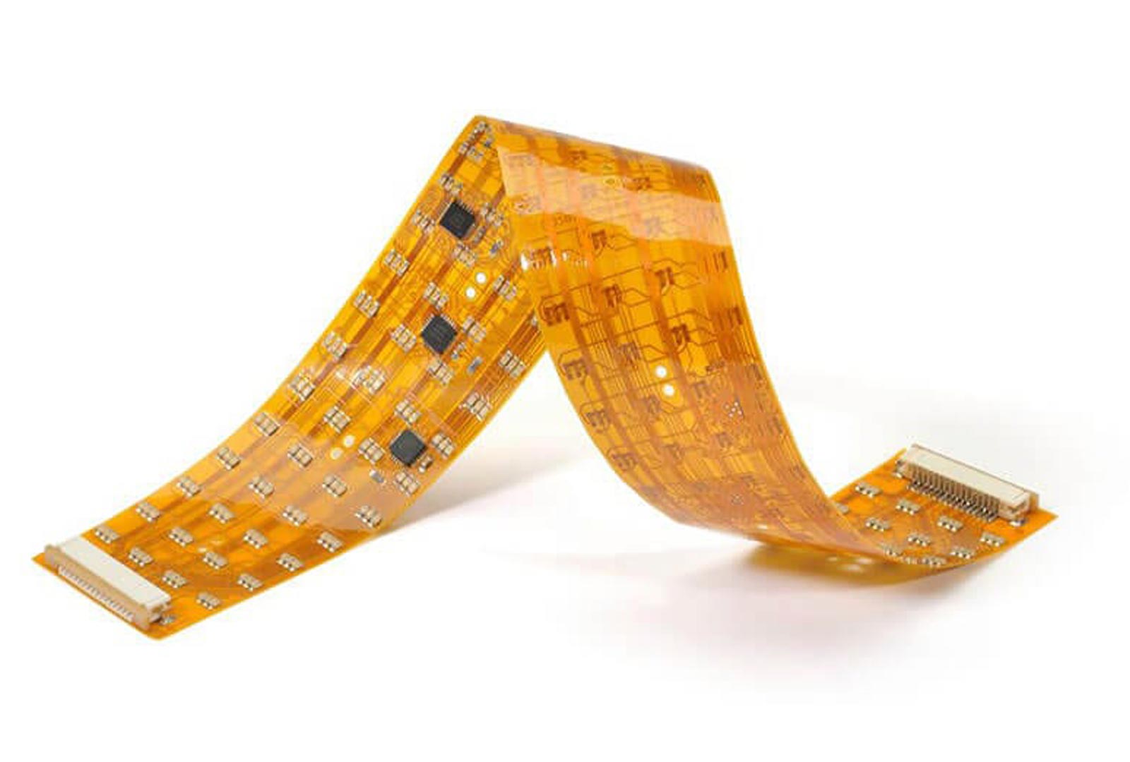
How to Evaluate an Australia PCB Manufacturer’s Lead Time?
1. Clarify Lead Time Definitions & Baselines
- Distinguish between prototype and mass production lead times.
- Confirm standard lead time ranges (e.g., prototypes: 24hrs–7 days; mass production: 10–25 working days).
- Verify if lead time includes design review, production, testing, and shipping.
- Check for minimum order quantity (MOQ) impact on lead time (e.g., no extra delay for small batches <50 units).
2. Evaluate Production Scheduling & Capacity
- Ask about current production capacity utilization rate (ideal: 70%–90%).
- Inquire about peak season lead time adjustments (e.g., +3–5 days during Q4).
- Confirm availability of dedicated production lines for urgent orders.
- Check if the manufacturer uses ERP systems for production planning.
3. Assess Supply Chain Reliability
- Verify lead times for key raw materials (FR4, copper, solder mask) from local Australian suppliers.
- Ask about backup suppliers for critical components (to avoid material shortages).
- Check if the manufacturer maintains safety stock for common materials.
- Evaluate proximity to component suppliers (reduces shipping delays within Australia).
4. Validate Process Efficiency & Automation
- Inquire about automation level (e.g., automated drilling, soldering, inspection).
- Check for in-house testing capabilities (e.g., AOI, X-ray, functional testing) to avoid outsourcing delays.
- Ask about design for manufacturing (DFM) review turnaround time (<24hrs ideal).
- Verify if the manufacturer offers expedited production options (e.g., 24hr prototype service).
5. Review Communication & Transparency
- Confirm real-time order tracking system availability (e.g., online portal, email updates)
- Ask about delay notification protocols (e.g., 48hr advance warning with root cause)
- Check if the manufacturer provides a dedicated account manager for lead time queries
- Verify response time for lead time-related questions (<1 business day)
6. Verify Past Performance & References
- Request lead time data for similar PCB projects (e.g., 10-layer HDI boards)
- Ask for customer references to confirm on-time delivery rates (>95% ideal)
- Review case studies for high-volume or time-sensitive orders
- Check if the manufacturer has penalties for late deliveries (e.g., discount on next order)
7. Account for Customization & Special Requirements
- Confirm lead time adjustments for custom specs (e.g., impedance control, gold plating: +2–3 days)
- Inquire about lead times for special PCB types (rigid-flex, metal-core, halogen-free)
- Check if international certifications (IPC, RoHS) add to lead time
- Verify shipping timeframes within Australia (e.g., 1–3 days via express courier)
Frequently Asked Questions
Q1: What’s the typical turnaround time for PCB prototyping?
A1: Our standard prototyping lead time is 1–5 days, with 24–48 hour expedited options available for urgent projects. This is 50% faster than average overseas lead times .
Q2: How do you ensure PCB quality for medical or defense applications?
A2: We follow IPC-A-600 Class 3 standards and maintain ISO 13485 certification for medical devices. Every batch undergoes X-ray inspection, thermal cycling tests, and traceability documentation .
Q3: Can you handle custom PCB designs that require unique materials?
A3: Yes, our engineering team works with specialized materials (e.g., high-frequency RF substrates, flexible polyimide) and can source custom materials through our global network, with local stock for common options .
Q4: How do your prices compare to overseas manufacturers?
A4: While our unit prices may be 10–15% higher for large batches, the total cost of ownership is lower due to faster delivery, no customs fees, and minimal rework costs. For small batches, we’re often more cost-effective .
Q5: What happens if a PCB fails during testing?
A5: We offer a 100% quality guarantee—if a PCB fails due to manufacturing defects, we’ll rework or replace it at no cost and expedite the new order to minimize your downtime