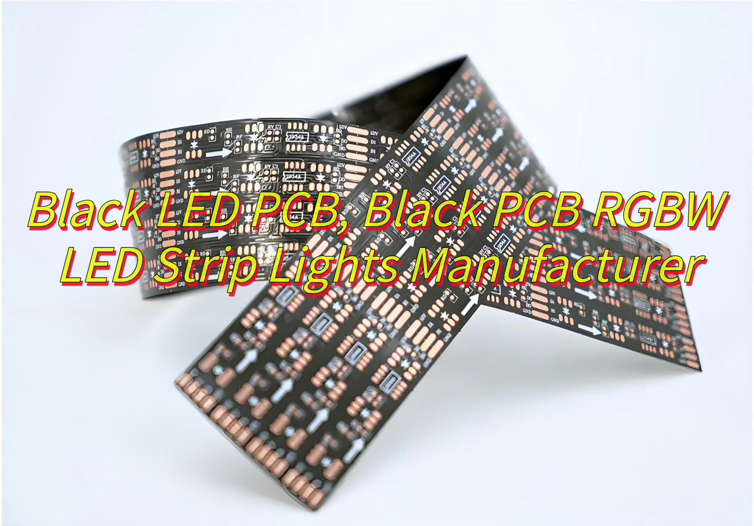
Seeking the ideal PCB for LED solutions? Explore its types, voltage conversion, China manufacturer selection tips, pricing and custom options like perforated round PCBs for Christmas holiday lighting.
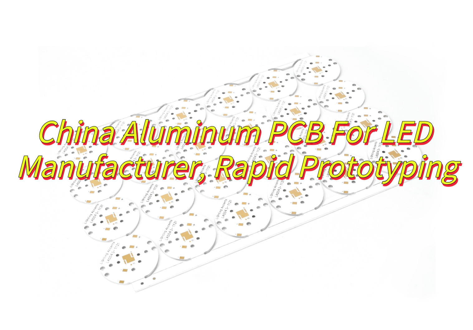
EBest Circuit (Best Technology) is a leading China aluminum PCB for LED manufacturer, offering unmatched 24-hour rapid prototyping to accelerate innovation. By utilizing in-house production facilities and advanced laser drilling technology, we deliver functional prototypes within one day—ideal for urgent LED projects requiring precise thermal management (up to 1.5W/m·K thermal conductivity). Our aluminum substrates minimize heat resistance (<2°C/W) for high-power LEDs, while automated SMT assembly ensures accuracy for compact driver designs. This capability is backed by rigorous thermal cycling tests (-40°C to +150°C) and ISO-certified processes, guaranteeing prototypes meet performance standards before mass production. Clients ranging from global LED lighting brands to startups benefit from our flexible solutions, including custom-shaped PCBs (e.g., perforated designs for holiday lighting) and multi-layer rigid-flex configurations. We streamline communication to align with your specs, whether for industrial tunnel lighting or residential applications, and support small-to-bulk orders with RoHS/UL-compliant materials. Trust our 16+ years of expertise to reduce time-to-market without compromising quality or cost-efficiency. Contact us today: sales@bestpcbs.com if you have any request for PCB for LED.
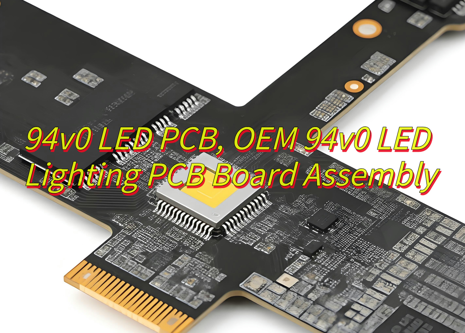
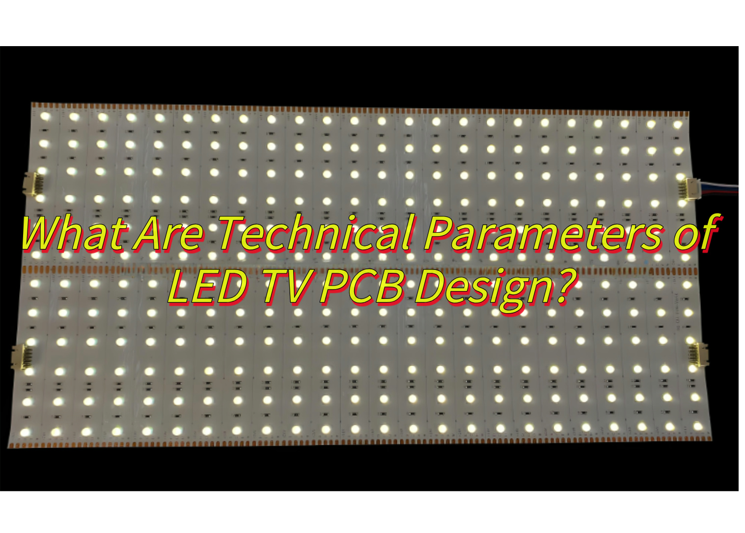
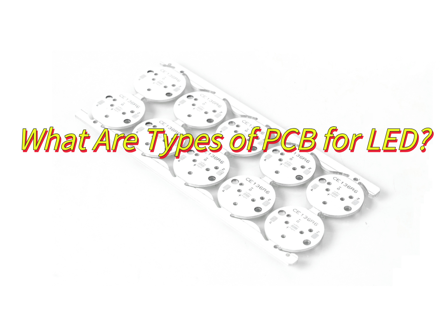
What Is PCB for LED?
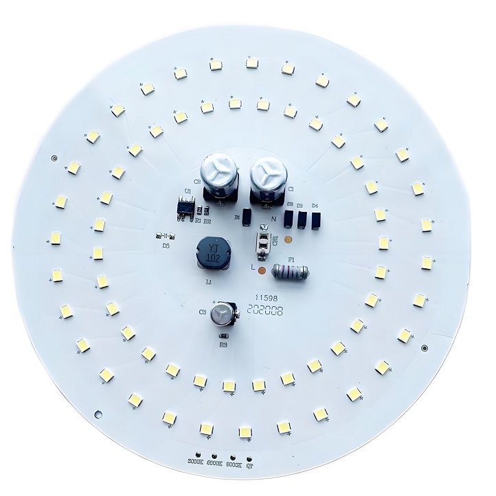
A PCB for LED (Printed Circuit Board for Light-Emitting Diode) is a specialized board designed to power, control, and optimize LED lighting systems. It serves as the structural and electrical foundation, connecting components like LED chips, resistors, and drivers while managing heat dissipation for stable performance. Aluminum-based PCBs are widely used in high-power LEDs (e.g., streetlights, automotive lighting) due to their superior thermal conductivity, while flexible PCBs enable compact designs for LED strips or decorative lighting. Critical features include precise circuit layout, material durability (e.g., FR4, ceramic, or metal-core substrates), and compatibility with SMD (Surface-Mount Device) technology. High-quality PCBs ensure energy efficiency, extended LED lifespan, and resistance to environmental factors like humidity or temperature fluctuations.
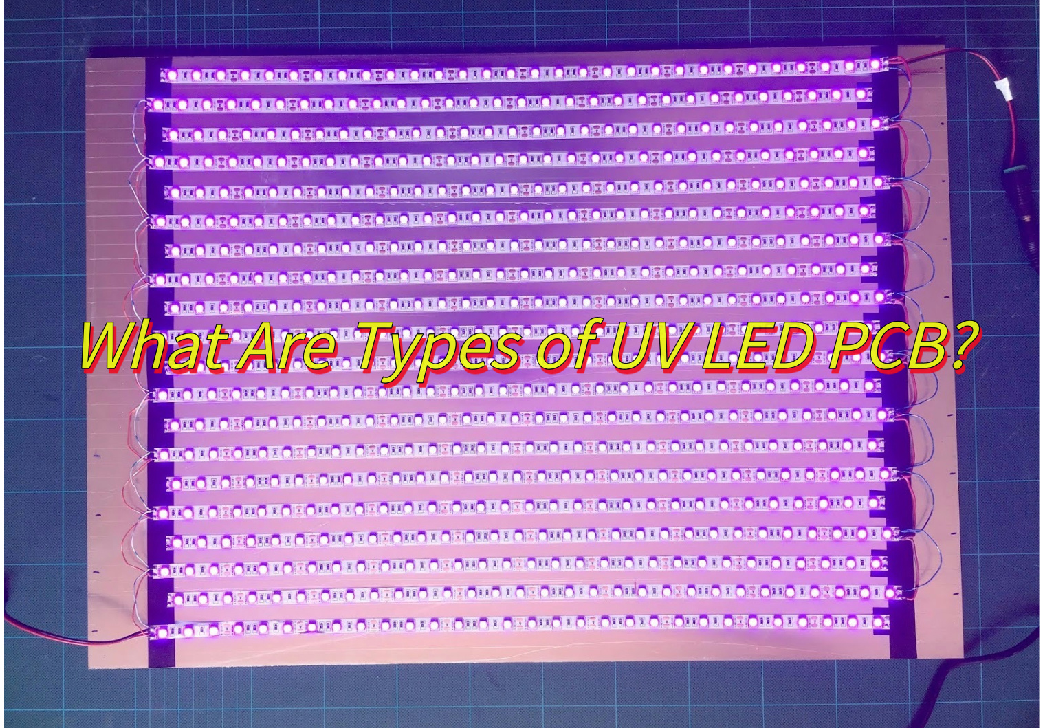
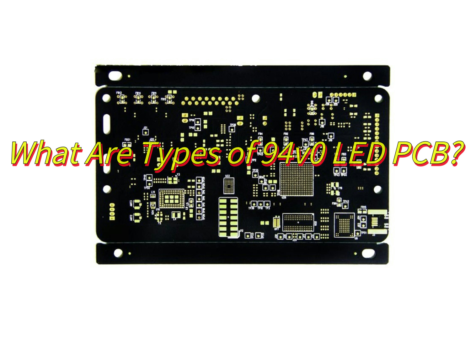
What Are Types of PCB for LED?
Types of PCB for LED:
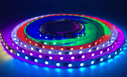
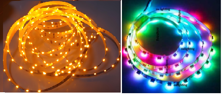
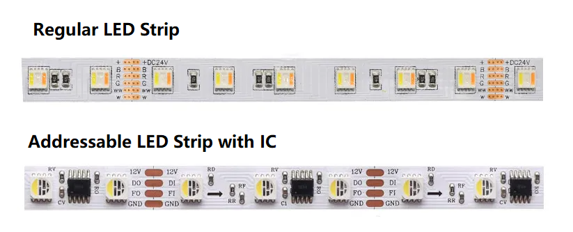
Flexible PCB for LED
- Design: Made from polyimide or polyester films, these thin, bendable circuits conform to irregular shapes.
- Applications: Ideal for LED strips, wearable lighting, and automotive interior lights where rigidity is a limitation.
- Advantages: Lightweight, vibration-resistant, and space-saving.
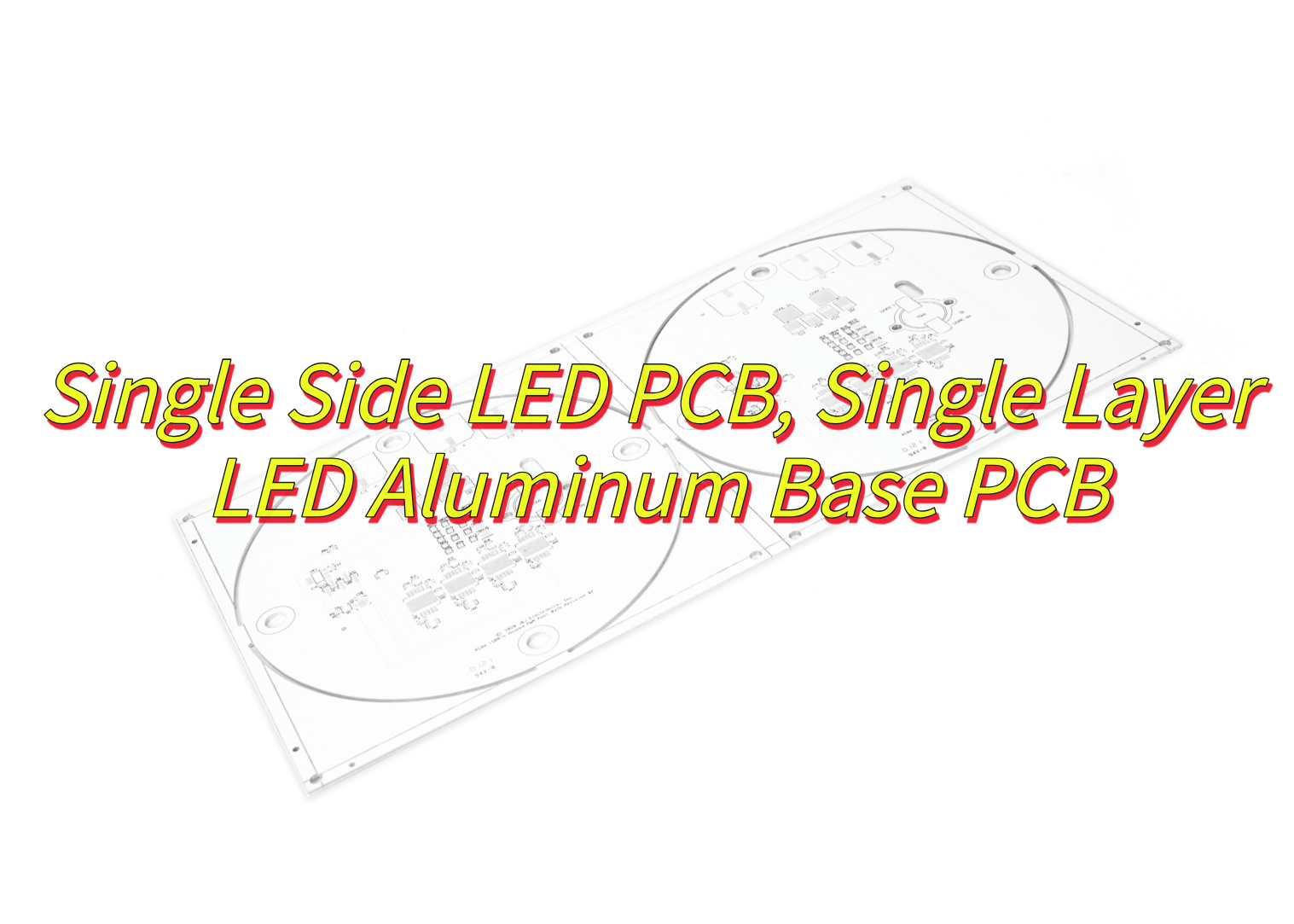
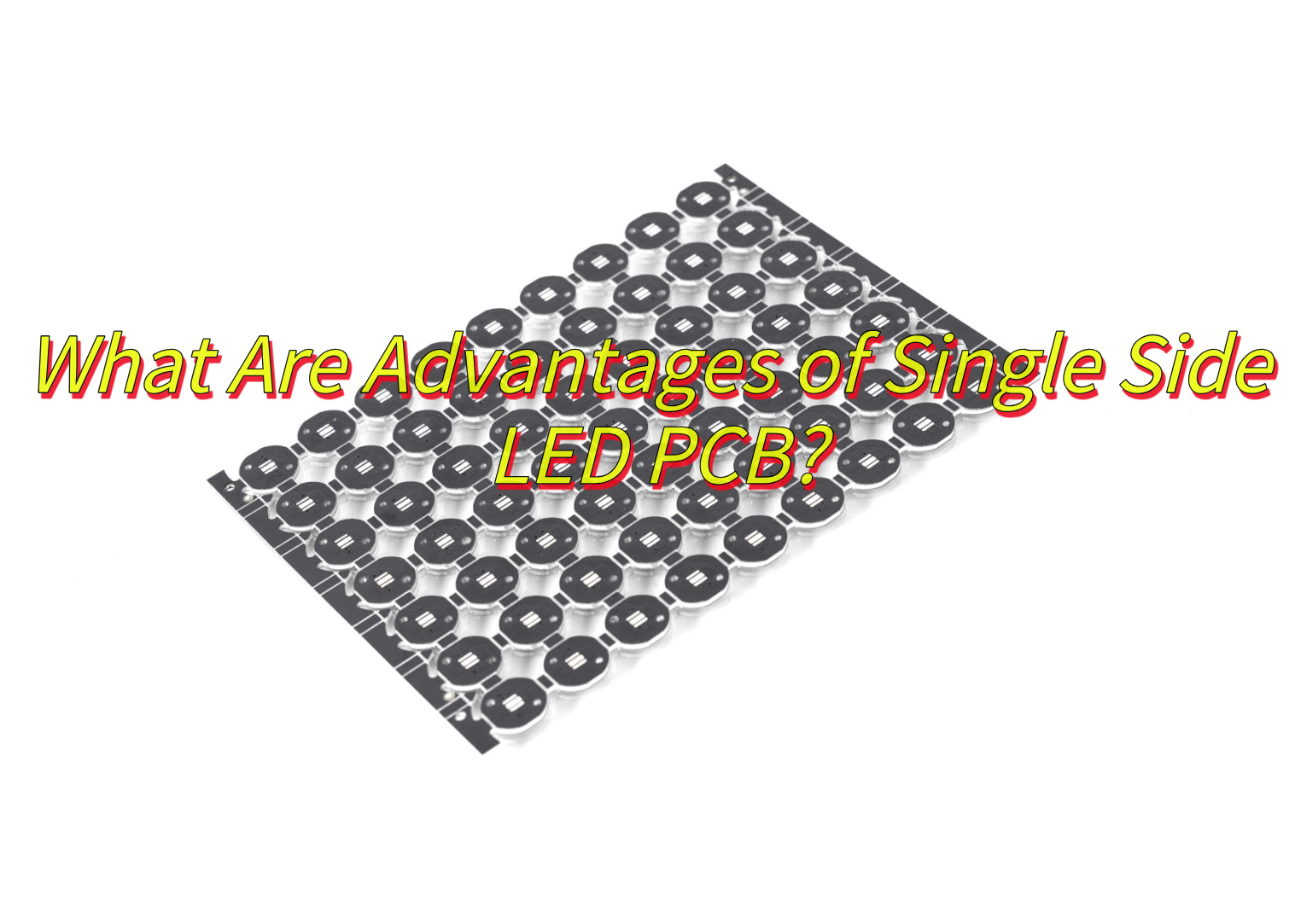
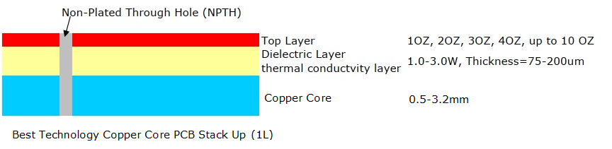
Aluminum Base PCB for LED
- Structure: Combines an aluminum substrate, dielectric layer, and copper circuit layer.
- Applications: Widely used in LED bulbs, streetlights, and high-power fixtures due to superior heat dissipation.
- Advantages: Reduces LED junction temperature by 30–50% compared to FR4, extending lifespan.
Ceramic PCB for LED
- Material: Typically alumina or aluminum nitride substrates.
- Applications: High-power LEDs, UV curing systems, and automotive headlights requiring extreme thermal stability.
- Advantages: Thermal conductivity up to 320 W/m·K, eliminating thermal runaway risks.
Metal Core PCB (MCPCB) for LED
- Variant: Includes copper or iron-based cores for specialized thermal management.
- Applications: LED grow lights, industrial floodlights, and architectural lighting.
- Advantages: Balances cost and performance for mid-to-high-power LED arrays.
Rigid-Flex PCB for LED
- Hybrid Design: Integrates rigid and flexible sections for 3D lighting configurations.
- Applications: Foldable LED displays, modular lighting systems, and aerospace applications.
- Advantages: Minimizes assembly steps while maintaining signal integrity.
High-TG FR4 PCB for LED
- Material: Flame-retardant glass-reinforced epoxy with high glass transition temperature (TG ≥ 170°C).
- Applications: Budget-friendly option for indoor LED panels and backlight units.
- Advantages: Cost-effective but less durable under prolonged high heat.
How to Convert Integrated 220v PCB for LED to 110v?
This is how to convert integrated 220v PCB for LED to 110v:
- Use a Step-Down Transformer – Connect a 220V-to-110V transformer between the power source and the PCB for LED. This method is straightforward and safe for low-to-medium-power LED systems (e.g., decorative or household lighting). Ensure the transformer’s wattage rating matches the total power consumption of the LED setup.
- Modify the Power Input Circuit – Adjust the PCB’s rectifier or voltage-doubling circuit. For example, if the original design uses a voltage-doubling configuration (common in 220V LED drivers), reconfigure it to a standard full-wave rectifier by disabling components like capacitors or diodes tied to voltage doubling.
- Replace the LED Driver – Swap the existing 220V LED driver with a 110V-compatible driver. This ensures proper voltage regulation and protects the LEDs from overvoltage damage. Verify compatibility with the PCB’s thermal and electrical specs.
- Update Filtering Components – Resize input capacitors and resistors to handle lower voltage. For example, reduce capacitor values in the EMI filter or surge-protection circuits to avoid overloading at 110V.
- Add a Voltage Stabilizer – Integrate a 110V AC-to-DC converter or switching power supply (SMPS) into the PCB for LED. This is ideal for high-power applications (e.g., streetlights) where stable voltage conversion is critical.
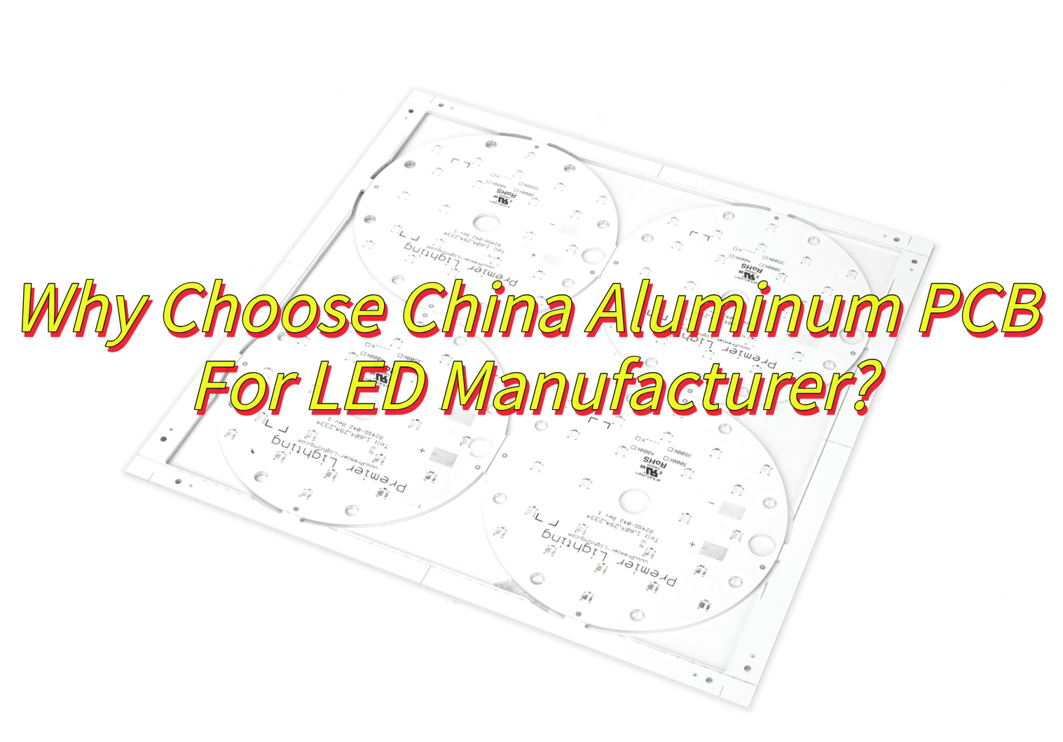
Why Choose China Aluminum PCB For LED Manufacturer?
China aluminum PCB for LED manufacturers have emerged as global leaders in producing high-quality PCB for LED applications, offering cost efficiency, technical expertise, and scalable solutions. Below are key reasons to partner with Chinese suppliers:
Cost-Effective Production Without Compromising Quality
- China’s mature manufacturing ecosystem reduces labor, material, and operational costs, enabling competitive pricing for aluminum PCB for LED products.
- Manufacturers balance affordability with precision, using advanced machinery like laser drills and automated optical inspection (AOI) systems to maintain tight tolerances (e.g., 0.075mm line spacing).
Advanced Thermal Management Expertise
- Aluminum PCBs excel in LED applications due to their superior heat dissipation. Chinese factories optimize dielectric layers (e.g., ceramic-polymer blends) to achieve thermal conductivity up to 3W/m·K, critical for high-power LEDs.
- Customized solutions include multi-layer designs (up to 36 layers) and heavy copper (12oz) for demanding applications like automotive headlights and industrial lighting.
Rapid Prototyping and Scalability
- Lead times for prototypes can be as short as 24 hours, with mass production starting within 5 days for orders below 500m². This agility supports time-sensitive projects.
- Facilities like Exceeding Electronics produce 50,000+ PCBs monthly, accommodating both small-batch trials and large-scale rollouts.
Stringent Quality Control
- Multi-stage inspections include AOI, X-ray for via integrity, and functional testing under extreme conditions (-40°C to 130°C).
- Certifications like UL 94V-0 (flammability), ISO 9001 (quality management), and RoHS (hazardous substance compliance) ensure reliability and regulatory adherence.
Customization Capabilities
- Tailored solutions include flexible-rigid hybrids, blind/buried vias, and via-in-pad technology for compact LED designs.
- Surface finishes like ENIG (immersion gold) and HASL-lead free cater to diverse soldering requirements, from automotive to consumer electronics.
Supply Chain Integration
- Vertical integration with raw material suppliers (e.g., aluminum substrate mills) minimizes lead times and price fluctuations.
- Proximity to semiconductor and LED chip manufacturers in regions like Shenzhen streamlines component sourcing.
Environmental Responsibility
- Factories comply with China’s strict environmental laws, using closed-loop water systems and VOC-free soldering processes.
- Recyclable materials and lead-free finishes align with global sustainability trends.
Global Compliance and Certifications
- Products meet standards like IATF 16949 (automotive) and ISO 13485 (medical), enabling entry into regulated markets.
- Third-party audits provide independent validation of quality and safety.
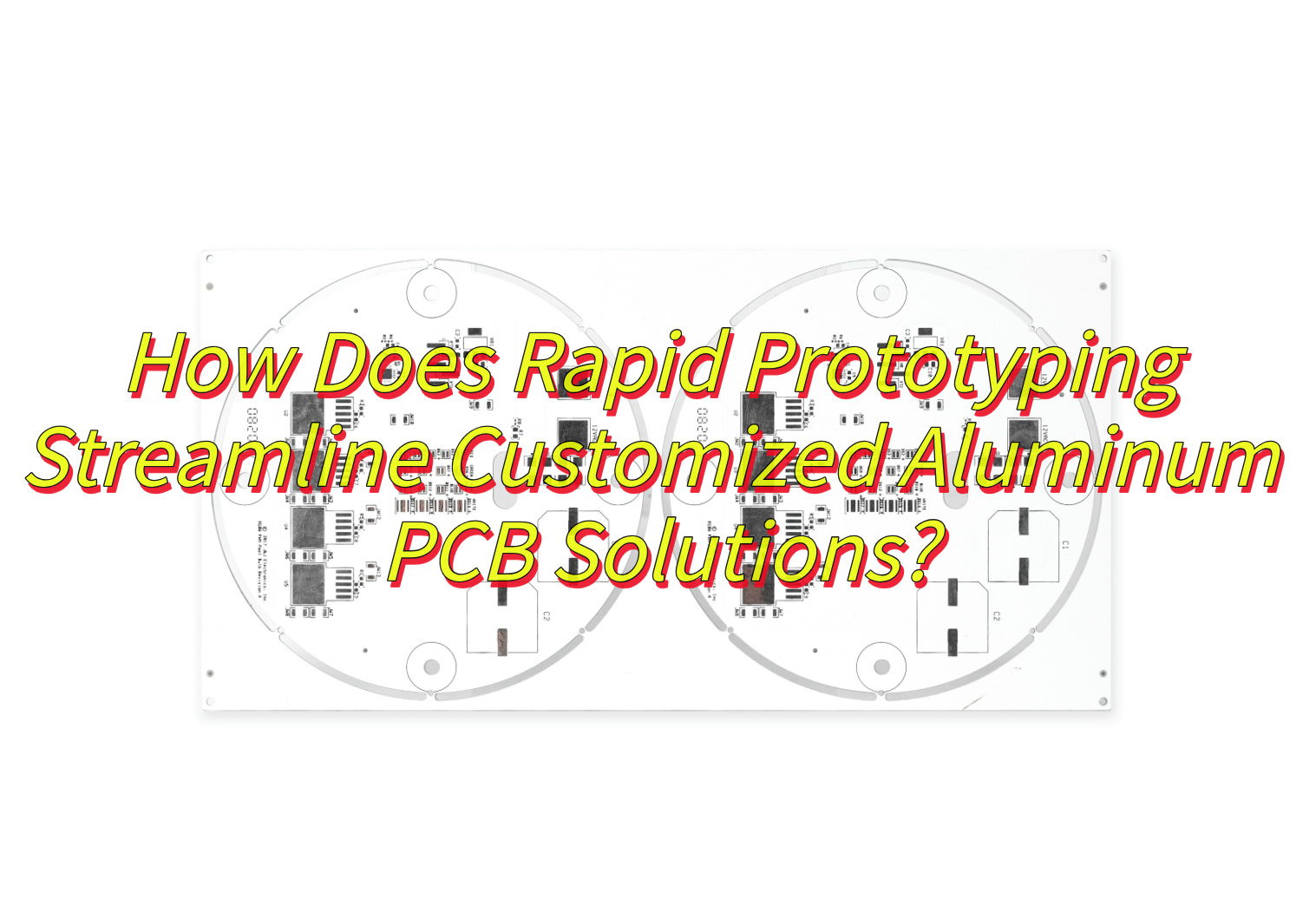
How Does Rapid Prototyping Streamline Customized Aluminum PCB Solutions?
Rapid prototyping simplifies the development of customized aluminum PCB for LED applications by condensing design cycles, reducing costs, and enabling iterative refinement. Below are actionable steps to streamline the process:
Leverage Pre-Engineered Design Templates
- Start with standardized aluminum PCB for LED layouts (e.g., 1.6mm core thickness, 2oz copper) optimized for common LED configurations (e.g., 5050 SMD, COB arrays).
- Modify only critical parameters (e.g., trace widths, thermal via patterns) to reduce design time by 30–50%.
Adopt Modular Material Kits
- Select from pre-qualified material stacks (e.g., 1.0mm aluminum + 0.1mm dielectric + 35µm copper) to bypass lengthy material certification.
- Pair with surface finishes like HASL-lead free for cost efficiency or ENIG for fine-pitch LEDs.
Automate Design for Manufacturability (DFM) Checks
- Use software tools to flag issues like insufficient annular rings or dielectric cracks before fabrication.
- Example: A DFM tool might auto-correct 0.15mm traces to 0.2mm to meet minimum etching requirements.
Use Laser-Direct Structuring (LDS) for Complex Geometries
- Skip traditional masking by directly etching circuits onto aluminum substrates using lasers, enabling 3D designs in <4 hours.
- Ideal for LED heatsinks with embedded lighting paths or automotive DRL modules.
Parallel Thermal and Electrical Testing
- While prototyping, simulate LED junction temperatures using thermal cameras and validate power efficiency with multimeters.
- Example: Test three dielectric variants (1.5W/m·K, 2.0W/m·K, 2.5W/m·K) in parallel to identify the optimal balance of cost and performance.
Implement Staggered Prototype Batches
- Order 5–10 units of each design variant to test in real-world conditions (e.g., high-humidity chambers for outdoor LED strips).
- Use results to eliminate underperforming designs before full-scale production.
Utilize In-House Rapid Soldering
- Test solderability of prototypes using selective soldering machines with nitrogen atmospheres to mimic mass-production conditions.
- Adjust stencil thickness (e.g., 0.12mm vs. 0.15mm) based on solder paste deposition results.
- Incorporate Feedback Loops
- After testing, revise designs using cloud-based collaboration tools and reorder corrected prototypes within 48 hours.
- Example: A LED grow light manufacturer reduced thermal via count by 20% after simulations showed marginal benefits beyond a certain density.
How Quickly Can You Deliver Rapid Prototyping for an Aluminum PCB for LED Strip?
The delivery timeline for rapid prototyping of aluminum PCB for LED strips depends on design complexity and manufacturer capabilities, but industry-leading processes can achieve 24–72 hour turnarounds using optimized workflows. Below is a breakdown of timelines and customization shortcuts:
Design Submission & Pre-Analysis (2–4 Hours)
- Gerber File Review: Automated software checks for errors (e.g., trace gaps < 0.1mm, missing solder mask layers) within minutes.
- DFM Feedback: Instant recommendations for dielectric thickness (e.g., 0.1mm–0.3mm) or via placement adjustments to balance thermal and electrical performance.
Material Preparation & Laser Etching (8–12 Hours)
- Pre-Cut Substrates: Use standardized 1.0mm/1.6mm aluminum sheets with pre-applied dielectric layers to skip custom material sourcing.
- Laser Direct Structuring (LDS): Directly etch circuits onto the substrate, eliminating photomask steps and reducing lead time by 40%.
Surface Finishing & Solder Mask Application (4–6 Hours)
- Selective Coating: Apply HASL-lead free or ENIG finishes using spray robots for uniform coverage in <2 hours.
- Dual-Layer Solder Mask: Use liquid photo-imageable solder mask (LPI) for high-resolution LED pad definitions (e.g., 0.3mm pitch).
Electrical Testing & Thermal Simulation (2–4 Hours)
- Flying Probe Test: Verify continuity and isolation on 100% of nets without fixturing delays.
- Infrared Thermal Mapping: Capture heat distribution data in 15 minutes to validate LED junction temperature predictions.
Quality Assurance & Packaging (1–2 Hours)
- Automated Optical Inspection (AOI): Detect micro-cracks or dielectric delamination at 5µm resolution.
- ESD-Safe Packaging: Ship prototypes in vacuum-sealed bags with silica gel to prevent oxidation.
- Total Time: 17–28 hours for simple designs (e.g., single-sided LED strips). Complex multi-layer boards may require 48–72 hours.
What Is the Price of Aluminum PCB for LED Strip Rapid Prototyping?
The cost of rapid prototyping for an aluminum PCB for LED strip depends on specifications like size, layer count, and surface finish. Below is a realistic pricing breakdown based on industry standards:
Base Cost Factors
- Size: A 100mm × 10mm strip (common for 12V/24V LEDs) costs $15–$30 per prototype.
- Layers: Single-sided boards start at $15, while double−sided designs add $5–$10 for via drilling and insulation.
- Material: 1.6mm aluminum with 0.15mm dielectric layer adds $3–$5 compared to 1.0mm substrates.
Surface Finish Impact
- HASL-Lead Free: 0$–$5 (cost-effective for basic LED strips).
- ENIG (Immersion Gold): +$8–$12 (essential for fine-pitch 0.5mm LED pads).
- OSP (Organic Solderability Preservative): +$3–$6 (short-term storage only).
Add-Ons and Complexity
- Thermal Vias: $2–$4 per 100 via holes (improves heat dissipation by 15–20%).
- White Solder Mask: +$5–$8 (enhances light reflectivity for LED efficiency).
- Impedance Control: +$10–$15 (required for high-frequency LED drivers).
Volume Discounts
- 5–10 Units: $15–$30 each (ideal for testing dielectric thickness variations).
- 11–50 Units: $12–$25 each (cost per unit drops by 20–30%).
- 51+ Units: Negotiable bulk pricing (often <$10 per board).
Expedited Fees
- 24-Hour Turnaround: +50–100% surcharge.
- 48-Hour Turnaround: +30–50% (common for non-urgent projects).
Example Quote:
A 150mm × 12mm double-sided aluminum PCB for LED strip (1.6mm core, ENIG finish, 50 thermal vias) would cost:
- 5 Units: $25×5=$125 (24-hour delivery: $187.50).
- 20 Units: $20×20=$400 (48-hour delivery: $520).
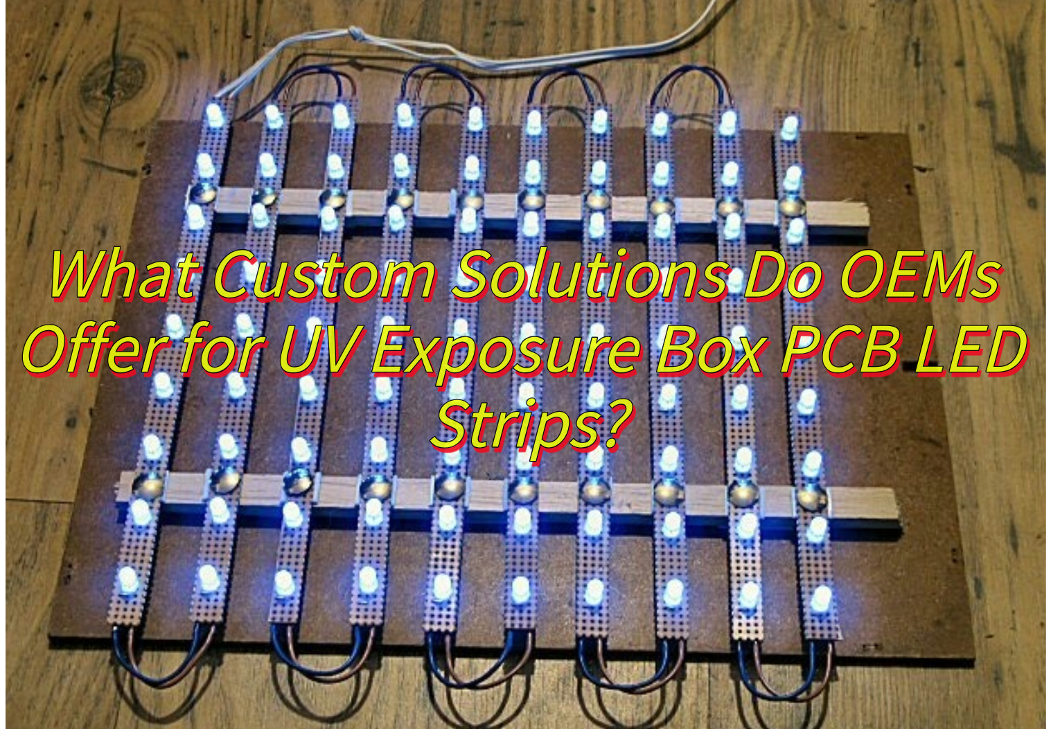
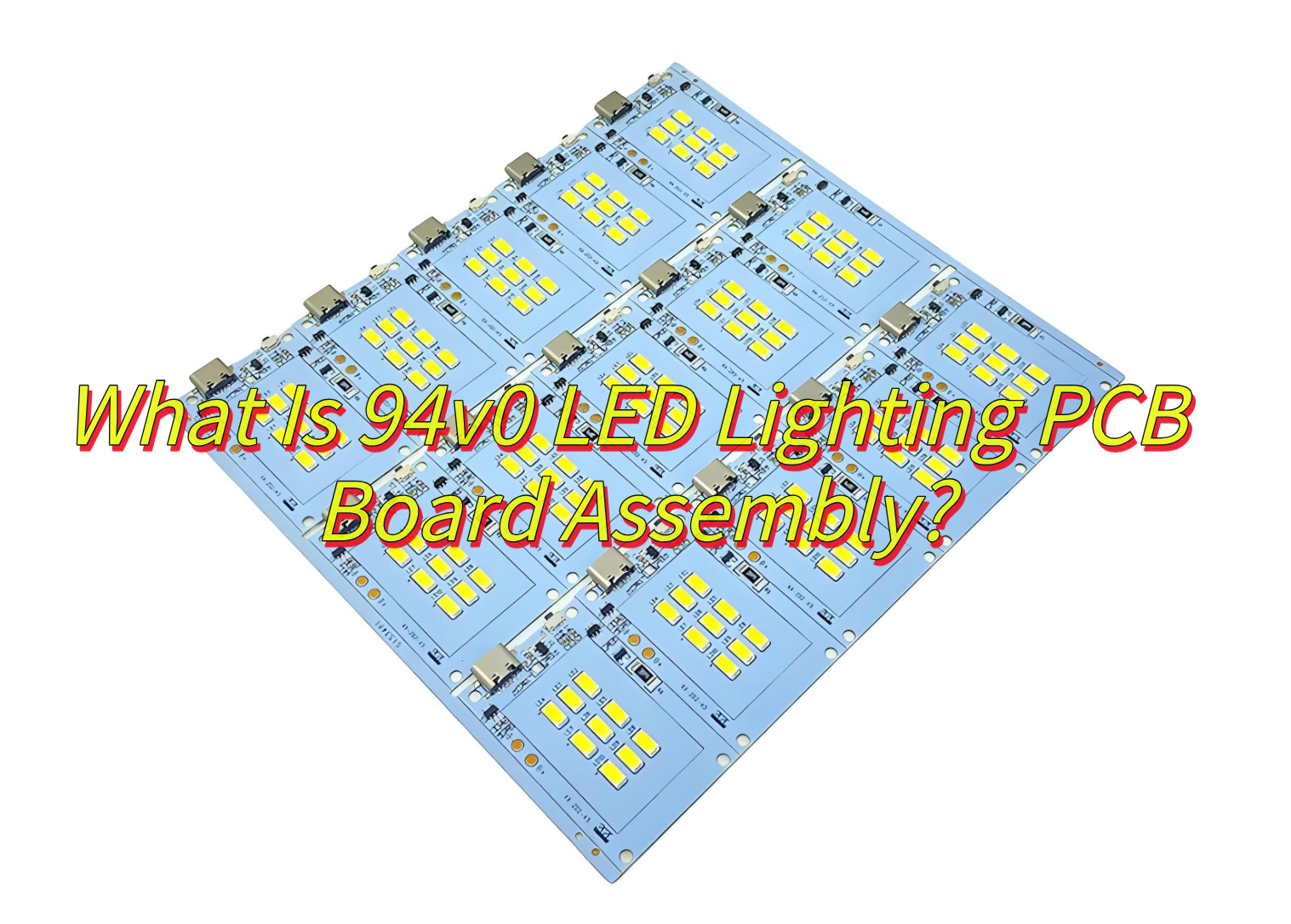
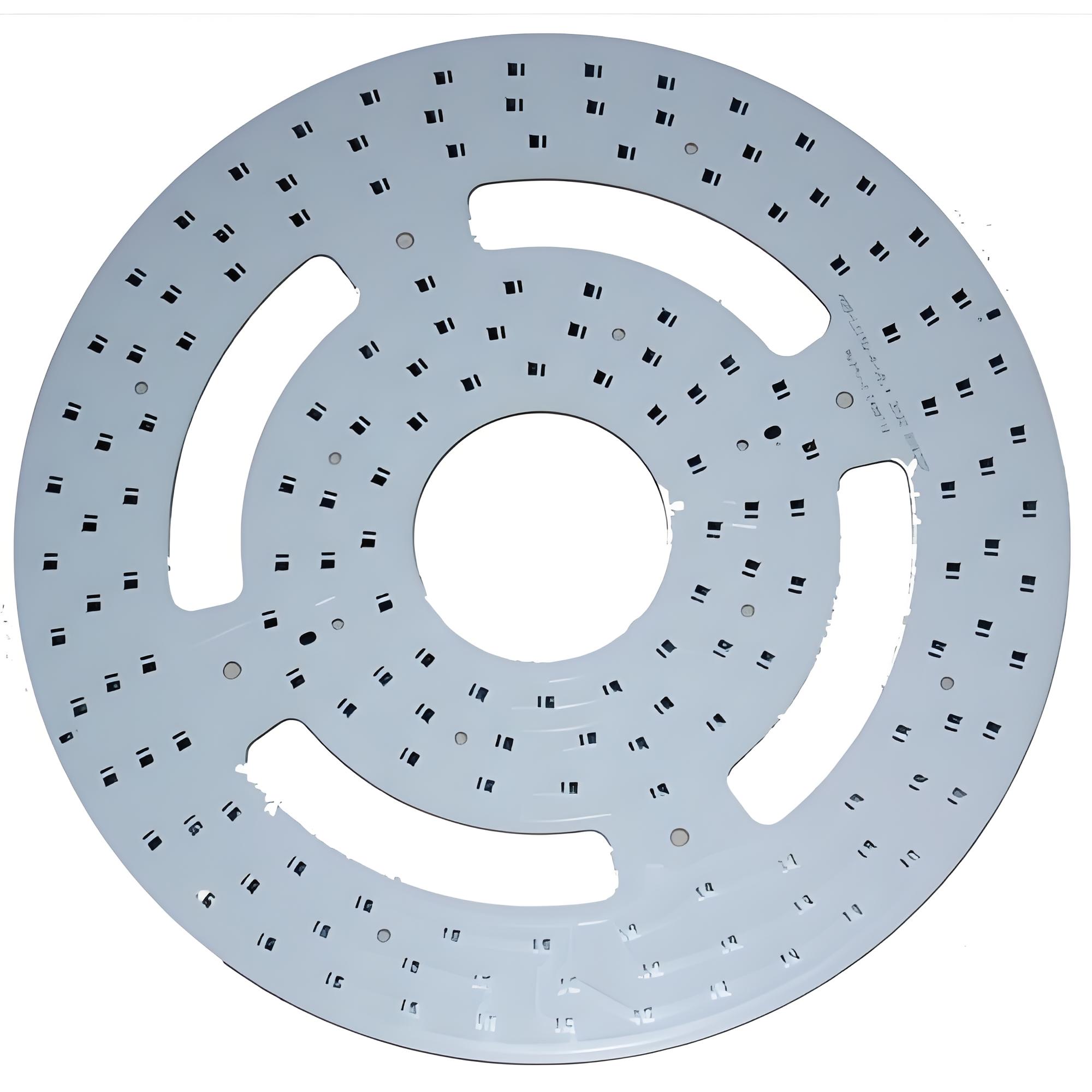
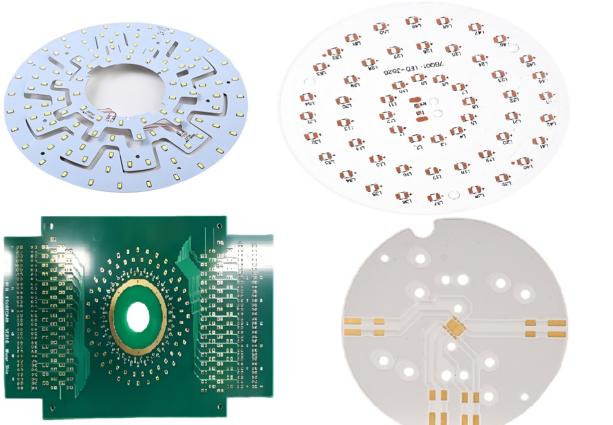
Can You Produce Perforated Round PCBs for LED Christmas Lights?
Yes, manufacturers can produce perforated round PCBs for LED Christmas lights. This capability is supported by modern PCB fabrication techniques, which allow for precise cutting, drilling, and finishing of circular boards with custom hole patterns. Below is a detailed explanation of the production process, pricing considerations, and practical advice for customers:
Production Feasibility
Modern PCB manufacturers utilize advanced technologies such as laser cutting, CNC milling, and mechanical drilling to create circular boards with perforations. These methods ensure accuracy even for intricate designs, including micro-vias as small as 0.2mm. Substrates like FR-4 (a cost-effective option) or aluminum-backed PCBs (for better heat dissipation in high-brightness LED applications) can be used, depending on performance requirements. Designs can be exported from standard software like Altium or Eagle, with manufacturers often requiring drilling templates for complex patterns.
Pricing Considerations
The cost of producing perforated round PCBs varies based on several factors:
- Order Volume: Smaller batches (1-10 units) typically range from 50to200 per unit due to setup and engineering costs. Medium batches (10-50 units) may cost 30to80 per unit, while larger orders (50-200+ units) can reduce the price to 15−50 per unit as economies of scale take effect.
- PCB Size and Material: Larger diameters (over 100mm) or thicker substrates, such as 1.6mm aluminum, can add 5−20 per unit. Flexible PCBs, though less common for LED Christmas lights, may incur a 30-50% premium.
- Perforation Complexity: High-density holes (less than 0.5mm pitch) or irregular patterns can increase costs by 10−30 per unit. Laser drilling for micro-vias may add 15-40% to the total cost.
- Surface Finish: Standard HASL (Hot Air Solder Leveling) is usually included in the base price, while ENIG (Electroless Nickel Immersion Gold) for improved solderability in dense LED arrays may add 10−30 per unit.
- Lead Time: Expedited production (3-5 days) typically carries a 20-50% surcharge compared to standard delivery (7-15 days).
Customization and Design Tips
- Hole Specifications: Hole diameter, spacing, and edge distances can be customized. Designs should comply with safety standards like UL588 for Christmas lights, ensuring flame resistance and proper strain relief for wire attachments.
- Thermal Management: Aluminum-backed PCBs enhance heat dissipation, extending the lifespan of high-brightness LEDs.
- Surface Treatments: Conformal coating can be applied for moisture resistance, especially for outdoor use.
Design Recommendations
- File Preparation: Provide detailed Gerber files with explicit drilling layers and mechanical annotations to ensure accuracy.
- Testing: Request electrical testing (e.g., flying probe) and thermal imaging to validate perforation integrity and thermal performance.
- Compliance: Confirm that designs meet relevant safety standards, such as UL588, to ensure product safety and marketability.
To sum up, that’s all content about PCB for LED’s types, voltage conversion, China aluminum PCB for LED manufacturer selection tips, pricing and custom options like perforated round PCBs for Christmas holiday lighting. Welcome to leave a message if you have any issues with PCB for LED.