Have you ever wondered what powers your mobile phone behind the screen? Every tap, swipe, or call you make is possible because of one hidden hero: the mobile phone PCB. In simple terms, the mobile circuit board connects and controls all parts of your phone. It links the battery, screen, camera, processor, and even your wireless network. Without it, nothing would work.
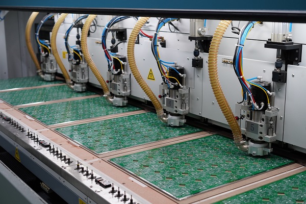
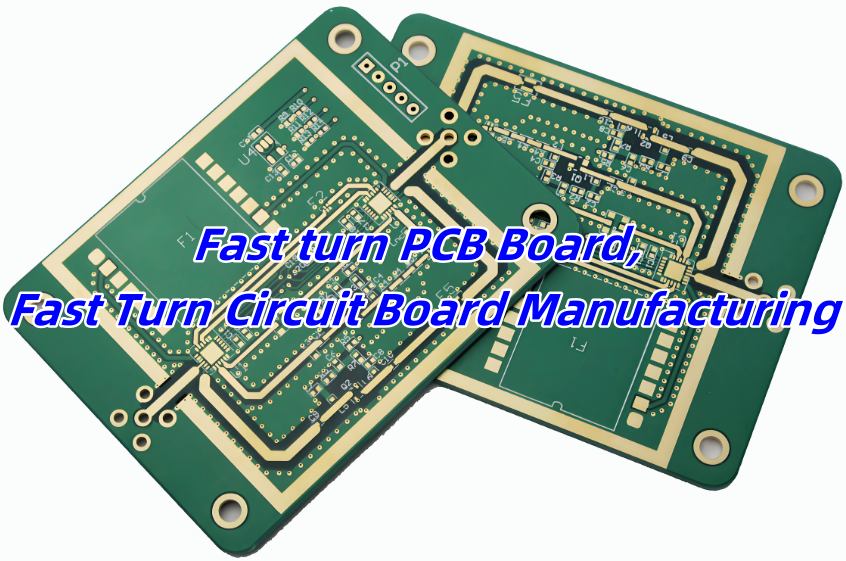
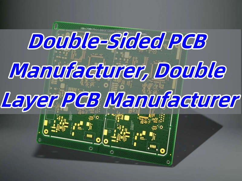
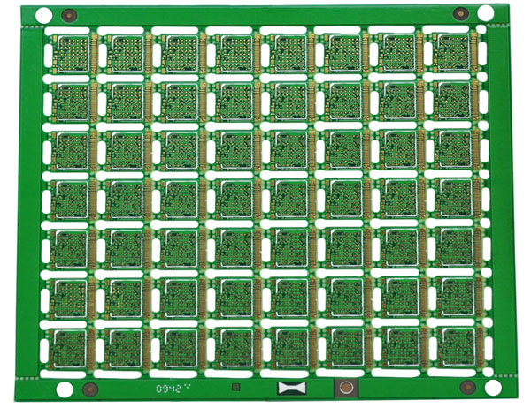
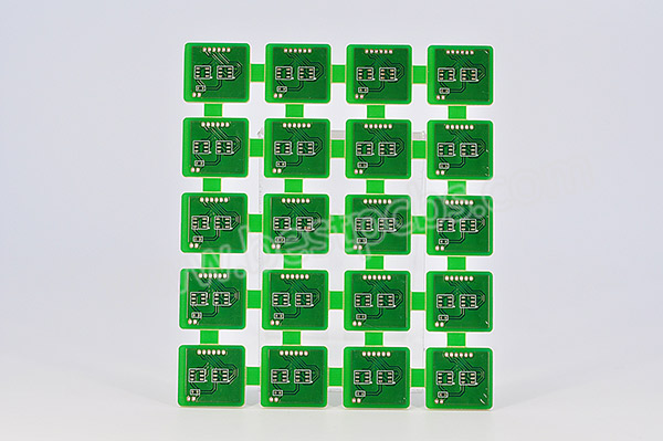
At EBest Circuit (Best Technology), we design and manufacture custom mobile PCBs that support today’s advanced smartphones. As a leading mobile PCB manufacturer both in China and Vietnam, we have decades years of experience in producing high-quality boards for mobile devices, wearables, and smart electronics. Certificated by ISO9001, IATF16949, ISO13485, AS9100D, it shows we have enough capability to produce highest quality mobile PCB board. Whether you need flexible, rigid, HDI, RF or multilayer PCBs, we deliver one-stop solutions with fast turnaround and competitive pricing.
What Is a Mobile Phone PCB?
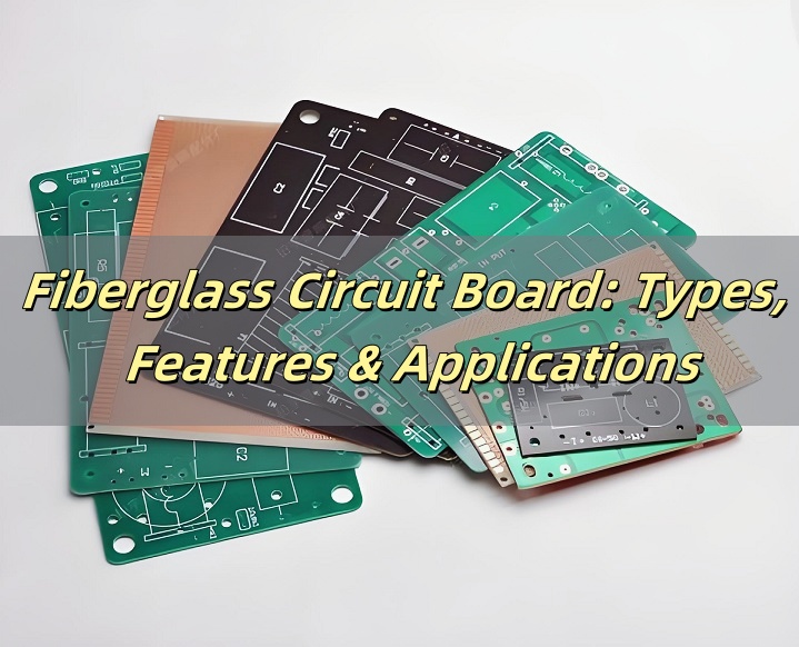
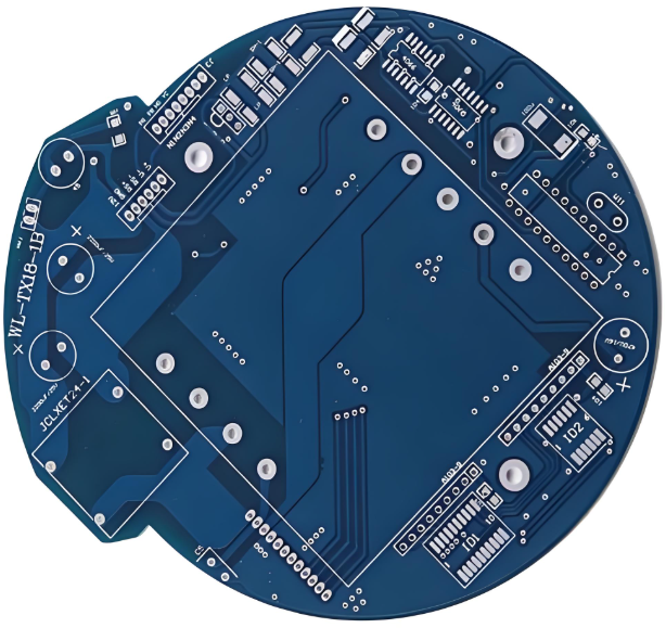
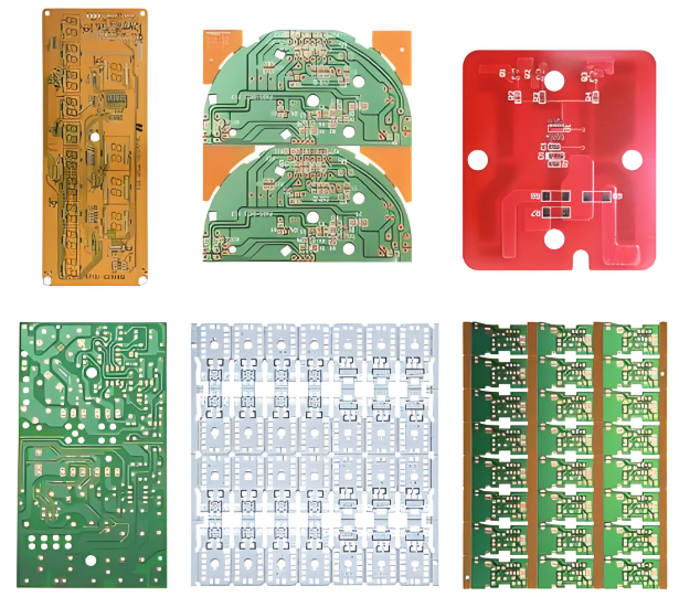
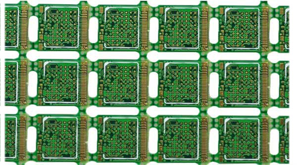
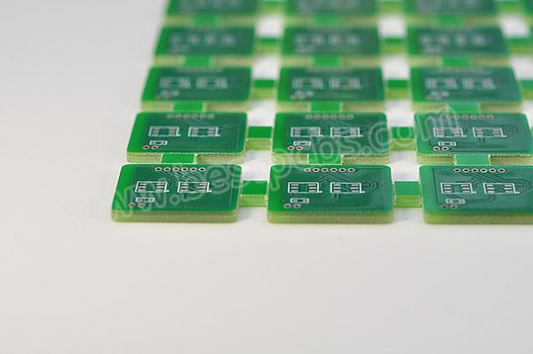
A mobile phone PCB is the core of your smartphone, which drives your phone be intelligent. It looks like a green or black plate populated with many small electronic parts. These components are connected through thin copper lines etched onto the board. Together, they power your phone and make sure each part works smoothly.
In smartphones, the PCB board mobile phone is usually a multi-layer board, meaning it has several layers stacked together. This design helps save space and supports high-speed data processing. The PCB also holds all essential parts like the processor, memory, charging port, and wireless chips.
What Does a Mobile Phone PCB Actually Do?
A mobile phone PCB acts like the brain and nervous system, it mainly used to connect and manage every part of the phone, its working principle is:
- Power distribution: It sends power from the battery to other parts.
- Signal transmission: It lets the processor talk to the screen, camera, and sensors.
- Component support: It holds everything in place and keeps them working together.
Without the mobile phone PCB, the battery wouldn’t know how to charge, the screen wouldn’t respond, and the speaker wouldn’t play music. It handles all the behind-the-scenes activity while you use your apps and make calls.
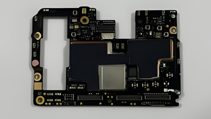
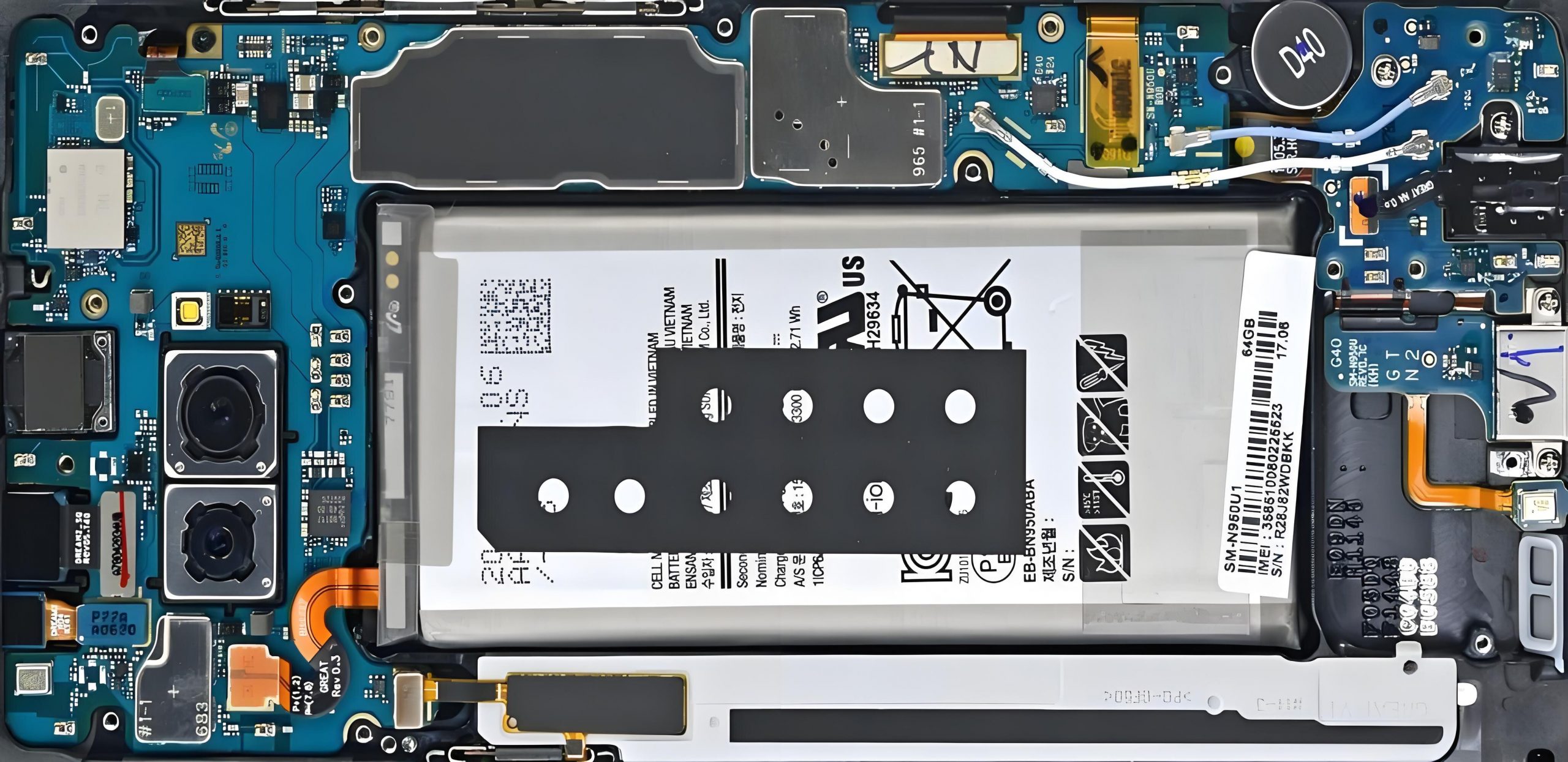
Core Components on a Mobile Phone PCB
A mobile phone PCB always is a populated PCB. At the top of the PCB, you’ll find the antenna point, where the antenna connects. Your phone connects to Wi-Fi, Bluetooth, and cellular networks through these antennas. Each component on the PCB plays its unique role:
- Antenna Switch: A 16-leg switch that controls signal direction. Sometimes built together with the PFO.
- PFO (Power Frequency Oscillator): Manages signal frequency. Found next to the antenna switch.
- Network IC: Controls mobile network functions. In some phones, it’s built into the CPU.
- Power IC: Found near brown capacitors. Regulates power across the PCB.
- CPU (Processor): The largest IC. Handles all system commands and performance tasks. Some phones have two CPUs.
- Flash IC: Stores system data and software. Located beside the CPU.
- Logic IC: A 20-pin chip. Manages basic logic operations.
- Charging IC: Found beside R22. Controls battery charging.
- Audio IC: Controls sound functions. Placed close to the Power IC.
- Capacitors: Store and release electrical energy. Help stabilize power supply.
- Resistors: Control the flow of current. Protect other parts from too much power.
- Diodes: Allow current to flow in one direction only. Prevent power damage and signal errors.
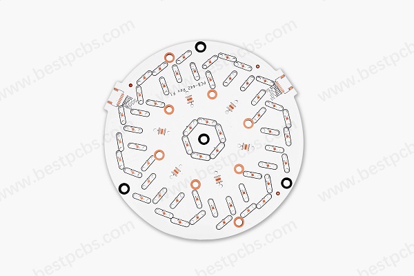
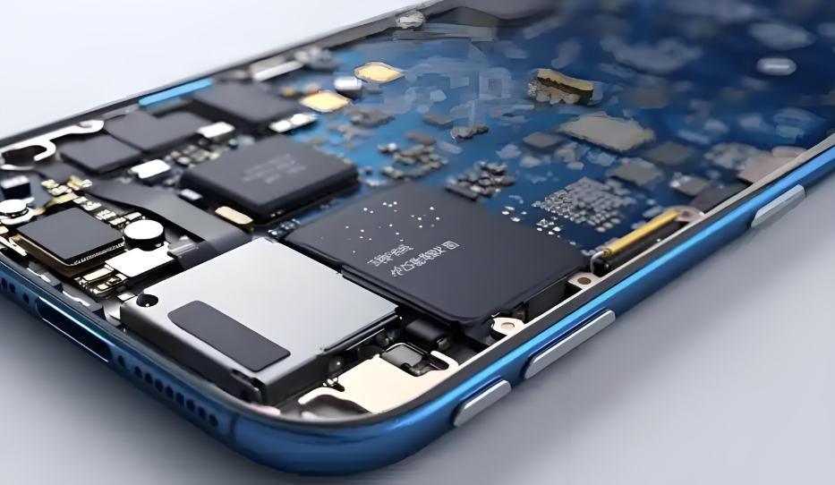
Below is a multi-layer PCB used in iphone. These parts make it possible for you to browse, take photos, and connect with the world.
Why Multi-layer PCBs Are Standard in Smartphones?
Today’s smartphones are like mini computers. They handle everything from streaming video to running powerful apps. To keep up, mobile phone PCB design has evolved. One of the biggest upgrades? The switch to multi-layer PCBs. Here we listing main advantages of using multi-layer PCBs in mobile phone.
Firstly, multi-layer PCBs offer higher circuit density, allowing more components like processors and memory to fit in the limited space. For example, the iPhone 14 Pro uses a 10-layer PCB to deliver powerful functionality in a compact design.
Secondly, they improve high-speed signal transmission by reducing interference through ground and shielding layers, ensuring stable and fast data transfer—a must for modern smartphones.
Additionally, multi-layer PCBs reduce the size and weight of smartphones. By accommodating more circuits in the same area, they help achieve smaller, lighter designs, like in the Apple Watch Series 8.
Finally, multi-layer PCBs enhance reliability and mechanical strength. Their complex construction improves durability and vibration resistance, ensuring a longer-lasting product.
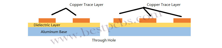
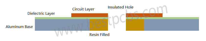
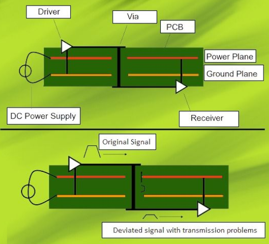
How Inner and Outer Layers Interact in a Mobile PCB Stack?
In a mobile PCB board, the inner and outer layers work together like a team. The outer layers handle the connection of chips, antennas, and components you can see. Meanwhile, the inner layers manage signal traces, power distribution, and ground planes.
Signals often travel between these layers through vias—small holes filled with metal that link one layer to another. This allows for faster, cleaner communication between the mobile PCB components, such as the CPU, RAM, and radio circuits.
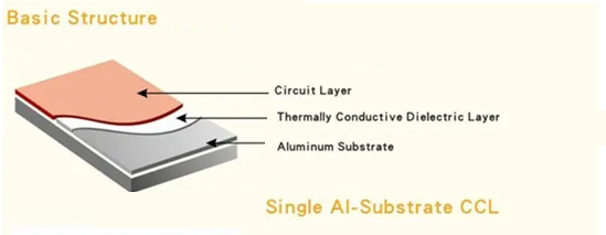
Materials Used in Mobile PCB Board
Choosing the right materials is crucial in mobile phone PCB manufacturing. Each layer and part of the board serves a different purpose, so engineers carefully select materials to match performance needs, durability, and size constraints. Here’s a comparison of commonly used mobile PCB materials:
| Material | Description | Pros | Common Use in Mobile PCB |
| FR4 | Fiberglass-reinforced epoxy laminate | Cost-effective, stable electrical properties | Base material in most mobile PCB cores |
| Polyimide | Flexible and heat-resistant material | Great for flexible PCBs and foldable applications | Used in camera modules, folding phones |
| Rogers | High-frequency laminate | Low dielectric loss, excellent RF performance | Antenna sections, 5G, Wi-Fi, Bluetooth |
| Teflon (PTFE) | Non-stick, high-performance polymer | Ultra-low signal loss, ideal for high-speed signals | Used in high-speed communication layers |
| Ceramic | Advanced inorganic composite | Excellent heat dissipation, high frequency stability | Power modules, 5G RF front-end, shielding |
PCB Layout Basics for Mobile Phones
A solid layout is the backbone of any mobile phone PCB. Designers start with the schematic, which maps every component and connection. Mobile PCB layout focuses on a few key goals:
- Short signal paths to avoid delay.
- Clear power and ground planes for stability.
- Thermal zones to manage heat.
- Shielded areas for RF sections like Wi-Fi and GSM modules.
- Placing the processor, RAM, power management ICs, and antennas carefully prevents problems later.
Warm tips:
Keep power and ground layers as solid planes. Avoid breaks or thin sections, which create voltage drops. Also, decoupling capacitors should sit close to power pins of chips.
Tips for GSM, Wi-Fi, Bluetooth, and 5G Mobile PCB Antennas
- Keep antennas away from metal—metal blocks signals.
- Use ground clearance around antenna traces to reduce noise.
- Match impedance of the RF trace to avoid reflection.
- Add shielding near high-speed digital lines to prevent signal loss.
For 5G, which uses millimeter-wave bands, the routing must be super precise. Even a few millimeters can affect signal strength. Tools like electromagnetic simulation software help refine these paths.
How AI and Automation Are Changing PCB Layout?
AI and automation have brought big changes to mobile PCB design in this two year. Instead of placing parts manually, designers can now rely on smart layout tools that optimize paths automatically. Machine learning predicts optimal routing paths. Automation assists in component placement, thermal analysis, and EMI reduction. They suggest better placements in seconds—saving hours of work.
AI also speeds up mobile PCB testing. It spots defects on boards using image recognition. That means more accurate inspections, less rework, and faster production.
As AI tools improve, they’ll continue to reduce errors, cut costs, and deliver better mobile board designs. It’s a leap forward for the industry.
What Does EBest Circuit (Best Technology) Serve You?
At EBest Circuit (Best Technology), we provide complete solutions for mobile PCB design and manufacturing. Whether you’re developing a new smartphone, tablet, or wearable device, we help you build it from the ground up. Our services including but not limited to:
- Custom mobile phone PCB layout and design based on your needs
- Single-layer to 32+ layer boards, including HDI, rigid-flex, and high-frequency options
- Advanced material selection such as FR4, polyimide, Rogers, and BT epoxy
- Rapid prototyping and small-volume production with quick delivery
- Full testing services like AOI, flying probe, impedance, and X-ray inspection
With over 18 years in the PCB industry, we’ve supported top-tier brands in building reliable, high-performance mobile electronics. Our team works closely with customers and give the best suggestions to optimize your mobile circuit board design. If you are interested in the mobile PCB develop, you are welcome to contact our team at sales@bestpcbs.com.
FAQs
1. What does a mobile phone PCB diagram show?
It shows where each component is placed on the board and how they are connected through copper traces.
2. How can I avoid power issues in PCB layout?
Use ground planes, short power paths, and place capacitors close to chips for voltage stability.
3. How do I identify damaged parts on a mobile PCB?
Use thermal cameras, multimeters, and reference schematics to locate shorted, burned, or faulty components.
4. What makes EBest Circuit (Best Technology) a strong mobile PCB manufacturer?
They provide full-stack design-to-production all in one service, expert engineering support, DFM check, SI, PI analysis and a proven track record in mobile electronics.