Struggling to find the right PCB manufacturer in France? This guide covers top manufacturers, pain points, selection tips, capacity and lead time evaluation, industry challenges, and FAQs.
When seeking reliable PCB solutions in Europe, understanding the top 10 PCB manufacturers in France is crucial for making informed decisions. The PCB Manufacturer in France sector boasts a mix of established local enterprises and international players, each with unique strengths in technology and service. Exploring the top 10 PCB manufacturers in France not only helps identify suitable partners but also provides insights into the region’s industrial capabilities, quality standards, and market dynamics. This guide delves into detailed information about these manufacturers, core pain points of PCB manufacturer in France, selection advice, and key industry insights to support efficient and effective collaboration.

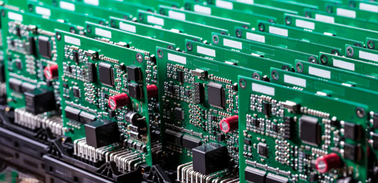
Top 10 PCB Manufacturer in France
| Company Name | Core Business | Process Capability | Lead Time |
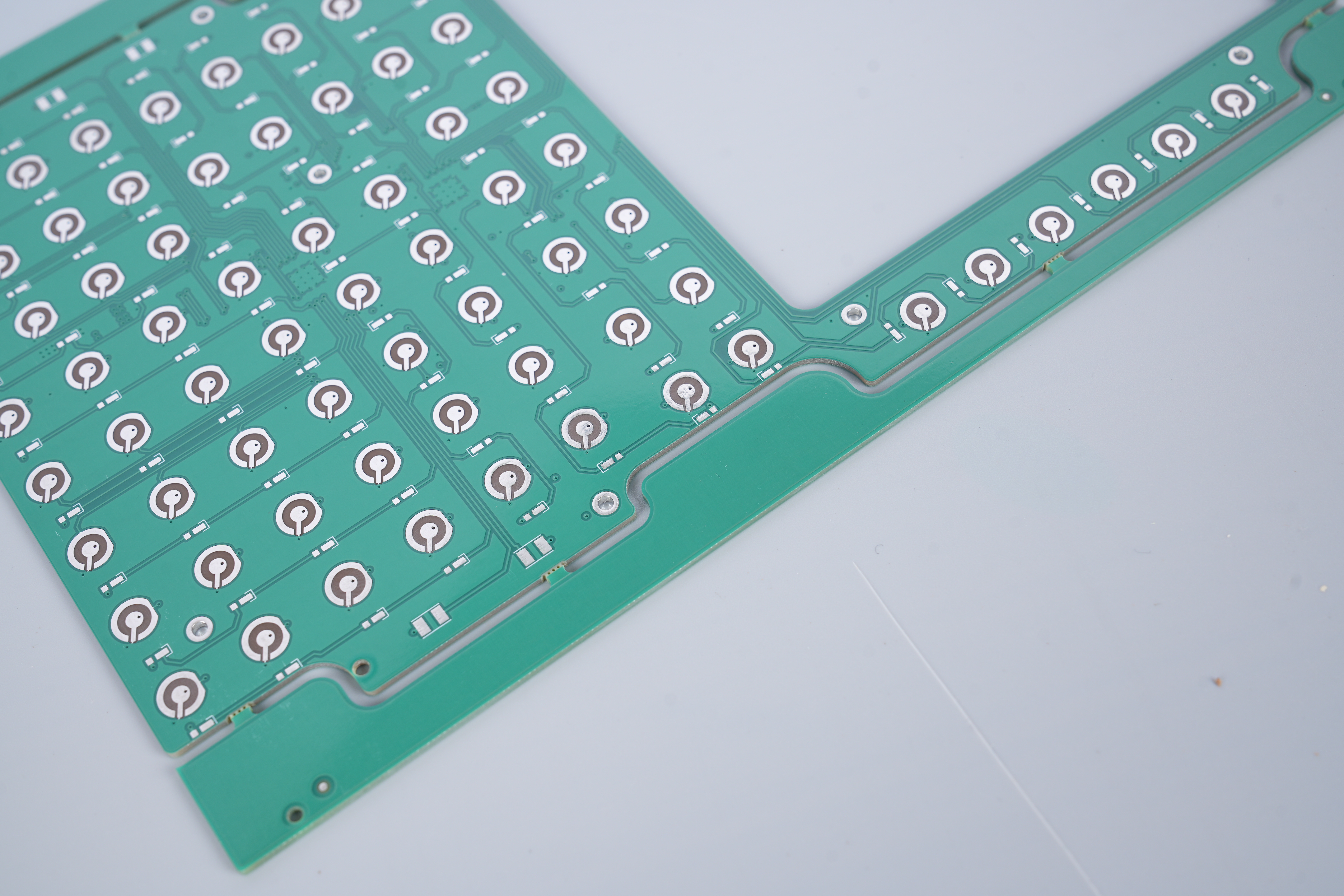
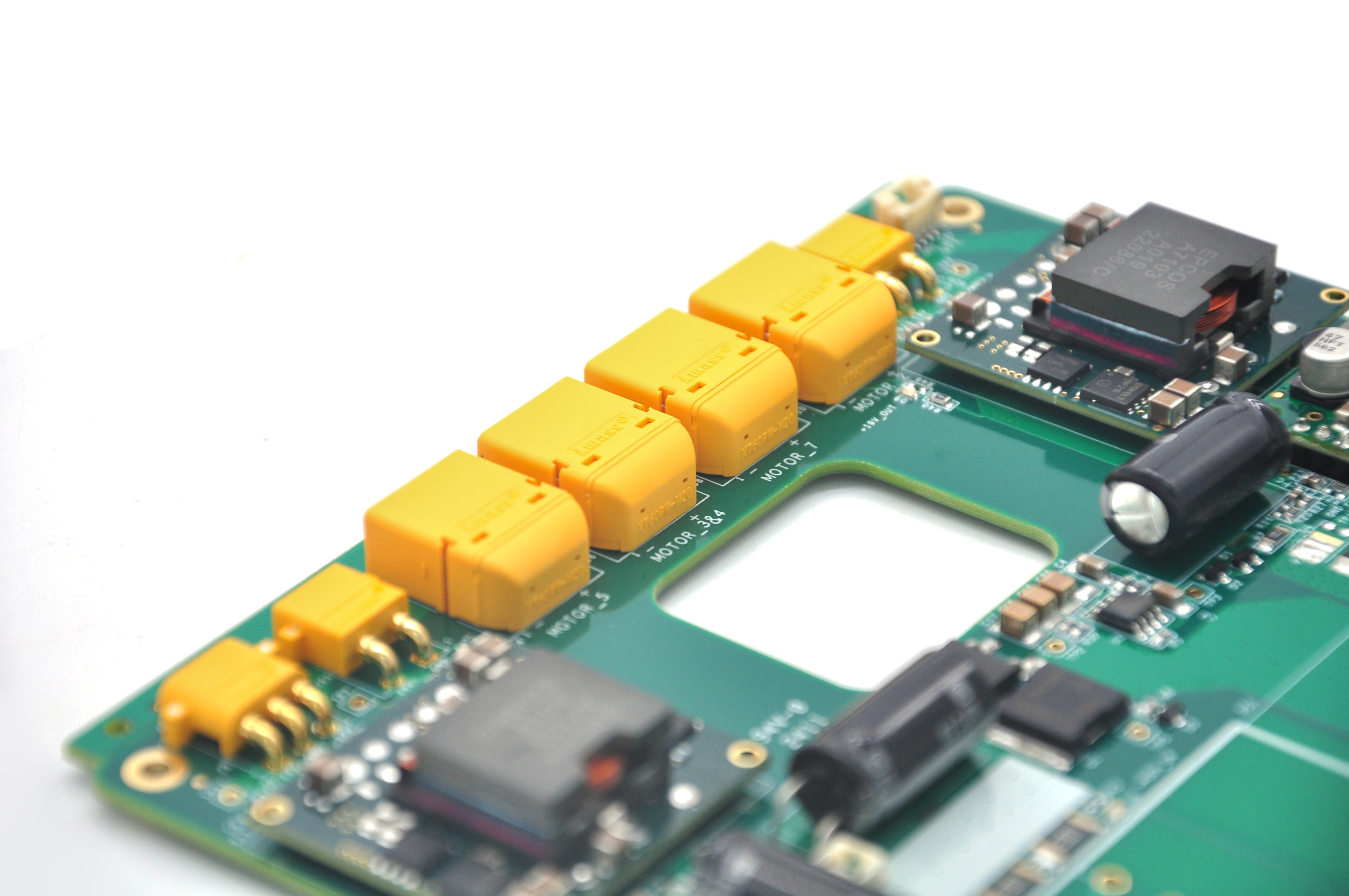
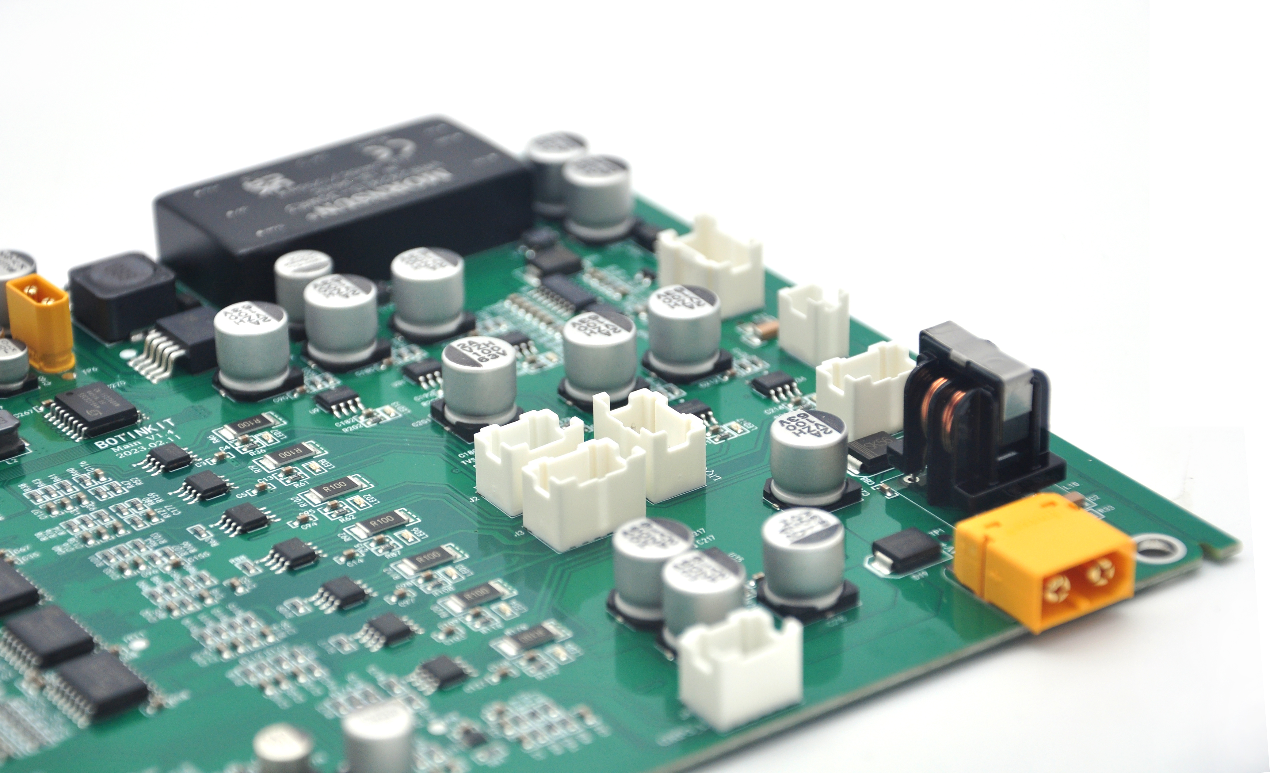
| EBest Circuit (Best Technology) | High-complexity PCBs (automotive, communications, EV charging) with design/manufacturing/assembly | 1-32 layers, flexible/ceramic/heavy copper, ±10% impedance, 18μm-6oz copper | Prototype 2-5 days, mass production 7-15 days, 97.2% on-time |
| Elvia Electronique | Aerospace/defense/medical/automotive/industrial high-precision PCBs | 1-32 layers, HDI, rigid-flex, aerospace-grade, ENIG/ENEPIG | Standard 10-20 days, aerospace 20-35 days |
| Group Icape | Telecom/industrial control customized PCBs (rigid/flexible/multilayer/metal core) | 1-24 layers, blind/buried vias, via-in-pad, 400mm×450mm max panel, ±10% impedance | Prototype 3-7 days, mass production 8-16 days |
| PCB Runner | HDI/metal core/high-speed/high-frequency rigid-flex PCBs | 1-32 layers, microvias, resin-plugged vias, ±10% impedance, RoHS | Expedited 2 days, standard 5-12 days |
| CSI Sud Ouest | European aerospace/defense critical PCBs | 1-24 layers, high-reliability, -40℃~125℃ thermal shock, CAF compliant | Standard 15-25 days, aerospace custom 30-45 days (post-fire rebuild) |
| Safe-PCB France | Industrial control small-batch customized PCBs | 1-16 layers, FR4, HASL/OSP, 0.1mm min line width | Standard 7-14 days, small-batch 5-10 days |
| Tech CI Rhones | Automation/telecom infrastructure multilayer PCBs | 1-20 layers, blind vias, ENIG, 3oz max copper | Standard 8-18 days, telecom 12-22 days |
| Pyliser Electronique | Custom profile (rectangular/circular) prototype/small-batch PCBs | 1-8 layers, FR4/TG170, 0.2mm min hole, solder mask custom | Prototype 2-4 days, small-batch 6-10 days |
| Synergie CAD | Industrial/medical rigid PCBs with design/manufacturing | 1-12 layers, ±10% impedance, RoHS 2.0, EN ISO 13485 medical | Standard 9-17 days, medical 18-28 days |
| TX Cube France | Communications/aerospace RF/high-frequency PCBs | 1-16 layers, high-frequency substrates, low-loss dielectric, ±8% impedance | Standard 12-20 days, high-frequency custom 20-30 days |
Pain Points of PCB Manufacturer in France
- High operating costs: Labor and production overheads in France are significantly higher than Asian competitors, with average manufacturing costs 35-40% higher than Chinese PCB manufacturers.
- Shrinking market share: Europe’s global PCB market share has plummeted from over 20% to just 2% in the past 15 years, with France accounting for a small portion of this declining share.
- Supply chain vulnerability: Over 82% of raw material demand for French PCB manufacturers relies on imports from Asia, leading to frequent supply delays and price fluctuations.
- Limited high-end technology capacity: Only a handful of French PCB manufacturers can produce ultra-high density interconnect (HDI) PCBs, failing to meet the growing demand for advanced electronics.
- Stringent environmental regulations: Compliance with EU RoHS 2.0 and REACH regulations increases production costs by 12-15% due to the need for eco-friendly materials and waste treatment.
- Low economies of scale: Most French PCB manufacturers have small production scales, with average monthly capacity below 50,000 square meters, leading to higher per-unit costs.
- Talent shortage: The declining PCB industry in Europe has led to a shortage of skilled technicians, with 60% of French manufacturers reporting difficulty in recruiting experienced production staff.
How to Choose A Reliable PCB Manufacturer in France?
Selection Guide to PCB Manufacturer in France:
1. Prioritize certified manufacturers
- Select enterprises holding valid ISO 9001 certification and industry specific credentials such as EN 9100 for aerospace applications and ISO 13485 for medical devices.
- Request to review certification validity documents and the latest surveillance audit reports to ensure compliance. Such certified manufacturers have been proven to have 40 percent fewer quality issues on average compared to non certified counterparts.
2. Evaluate equipment advancedness
- Confirm the adoption of high precision production equipment including LDI exposure machines and AOI detectors. For complex designs prioritize manufacturers that can demonstrate laser drilling precision of 0.1mm or better.
- Additionally verify equipment maintenance records to ensure consistent performance as well as the ability of LDI machines to achieve line width accuracy of ±5μm which is critical for high density designs.
3. Assess raw material supply stability
- Choose manufacturers with long term cooperative relationships with reputable material suppliers such as European based Isola and Rogers for substrates.
- Request to review the past three months of raw material inventory records to confirm they maintain 30 or more days of safety stock for common substrates like FR4. Also verify if they have dual supplier strategies for key materials to mitigate supply disruption risks.
4. Verify lead time credibility
- Compare the manufacturer’s quoted lead times against industry benchmarks. Standard double layer boards typically require 7 to 10 working days while 8 layer HDI boards need 15 to 20 working days.
- Request the manufacturer to provide delivery records of similar orders from the past six months to check the on time delivery rate which should be no less than 95 percent. Avoid manufacturers that promise lead times significantly shorter than industry norms as this often indicates compromised quality control.
5. Check quality control systems
- Require a detailed QC flowchart that covers the entire production process from incoming material inspection to final product testing. Key control points should include inner layer etching line width tolerance of ±10 percent solder mask alignment accuracy of 50μm or better and impedance testing for high frequency boards.
- Request to observe the QC process on site or review video records of inspection procedures to ensure strict implementation.
6. Evaluate production capacity flexibility
- Select manufacturers that maintain a 15 percent or higher capacity buffer for urgent orders. Request to review their order fulfillment records for the past year to check how they handled sudden demand surges such as orders exceeding normal monthly capacity by 15 percent.
- Confirm they have a formal urgent order processing mechanism that can ensure on time delivery without sacrificing quality standards.
7. Review after sales tracking capabilities
- Prioritize manufacturers that offer full batch number tracking which allows tracing of raw material sources production equipment used and inspection records for each batch.
- Ensure they provide a 12 month or longer quality guarantee with clear terms for defective product rework or replacement. Request to review their defect rate statistics which should be below 0.09 percent and confirm they have a 24 hour response mechanism for quality complaints.

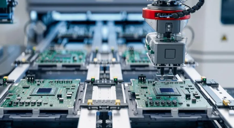
How to Evaluate Production Capacity of PCB Manufacturer in France?
Evaluation Guide to Production Capacity of PCB Manufacturer in France:
- Review monthly production capacity data: Focus on square meter output (target ≥10,000㎡/month for mass production needs) and product type coverage (multilayer/HD/flexible PCBs) .
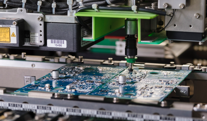
- Inspect production equipment lineup: Check the number and advanced level of key equipment (drilling machines, exposure machines, electroplating lines) and equipment maintenance records .
- Verify process certification and technical parameters: Confirm maximum layer count, minimum line width/hole diameter, and impedance control capabilities through third-party test reports .
- Evaluate sample production efficiency: Test the time required for prototype production (standard: 2-5 working days) and the consistency between sample quality and technical requirements .
- Assess supply chain management: Investigate raw material inventory levels, supplier qualification certificates, and emergency response plans for material shortages .
- Analyze historical order fulfillment data: Review on-time delivery rate (target ≥95%) and order completion rate for large-batch or complex projects .
- Inspect production site management: Evaluate 5S implementation, workflow optimization, and employee operation standardization through on-site visits or video inspections .
- Verify production process digitization: Check if MES production execution systems are used to enable real-time production progress tracking and data visualization .
How to Evaluate Lead Time of PCB Manufacturing Company France?
Evaluation Guide to Lead Time of PCB Manufacturing Company France:
- Clarify standard lead time benchmarks: For standard PCBs, double-layer boards typically take 8-12 working days. Establish industry-standard benchmarks to compare with manufacturers’ quoted lead times.
- Evaluate order complexity impact: Confirm lead time adjustments for high-layer count (16+ layers) or special material PCBs, which should not exceed 30 working days.
- Check raw material inventory status: Prioritize manufacturers with 45+ days of safety stock for key materials, reducing lead time delays caused by material shortages.
- Assess urgent order handling capabilities: Confirm if expedited services are available (target 3-5 working days for prototypes) and the additional cost ratio (should not exceed 50% of standard pricing).
- Verify production scheduling transparency: Choose manufacturers with visual scheduling systems that provide real-time updates on order progress and potential delay warnings.
- Evaluate logistics and transportation plans: Confirm cooperation with reliable logistics providers and alternative transportation schemes for cross-border deliveries.
- Check historical delivery performance: Review the past 12 months’ on-time delivery rate (minimum 93%) and the root cause analysis of past delivery delays.
- Clarify force majeure response mechanisms: Confirm lead time extension clauses and compensation policies for delays caused by factors such as natural disasters or policy changes.

Challenges Facing the PCB Industry in France
- Continuous industry shrinkage: Over 140 European PCB manufacturers have closed in 15 years, affecting France. Most French manufacturers operate below 70% capacity, facing profitability and client retention pressures.
- Intense global competition: Asian manufacturers (China, South Korea) offer 30-40% lower prices via large-scale production, capturing over 75% of the global mid-to-low-end market. French manufacturers are pushed to niche high-value segments.
- Stringent EU environmental policies: Complying with evolving EU regulations adds 15-20% to production costs, due to eco-friendly materials, wastewater treatment and carbon monitoring investments.
- Slow technological innovation: French manufacturers lag in advanced technologies like HDI and IC carrier boards. Only 3 out of 20 major French firms can produce HDI boards with line widths below 50μm, failing advanced electronics demand.
- Unstable supply chain: 82% of raw materials are imported from Asia, with frequent disruptions causing 10-15 day lead time extensions and 25% price volatility in two years.
- Talent drain: Young professionals avoid the sector, leading to an aging workforce. 60% of French manufacturers struggle to recruit skilled technicians, with average staff age over 48.
- Fluctuating market demand: 2.3% YoY growth in Europe’s electronics industry (2024) causes unstable orders, making long-term capacity planning difficult for French manufacturers.
- High energy costs: European electricity prices rose 65% since 2021, impacting energy-intensive processes (25-30% of total costs) and reducing small manufacturers’ profit margins by 12%.

FAQ About PCB Manufacturing in France
Q1: What is the typical lead time for PCB production, and how can I shorten it?
A1: Typical lead time: 7-10 working days for standard double-layer PCBs, 15-20 working days for 8-layer HDI boards. To shorten it, choose manufacturers with a 15%+ capacity buffer for urgent needs, provide complete and accurate design files upfront to avoid revisions, opt for expedited prototype services (2-5 working days), and confirm raw material availability in advance.
Q2: Are PCB manufacturers capable of producing high-frequency PCBs for aerospace applications?
A2: Yes, but only a few (e.g., Elvia Electronique, TX Cube) offer this capability. When choosing, confirm they use low-dielectric-loss high-frequency substrates, have ±8% impedance tolerance, and hold EN 9100 certification. Request thermal shock resistance (-40℃~125℃) and CAF test reports for reliability.
Q3: How to ensure PCB quality meets international standards?
A3: Prioritize manufacturers with ISO 9001, IPC-A-600, and industry-specific certifications. Request a detailed QC flowchart covering key points like ±10% line width tolerance and ≤50μm solder mask alignment. Conduct third-party testing on critical parameters such as impedance and high-temperature resistance. Review defect rate history (target <0.09%) and after-sales tracking systems.
Q4: Why are some PCB manufacturers more expensive than Asian ones, and is the price difference justified?
A4: The 35-40% price difference stems from higher labor costs, stricter environmental compliance, and smaller economies of scale. It is justified for high-reliability applications (aerospace, medical) due to better quality control, shorter European logistics lead times, and EU regulation compliance (RoHS 2.0, REACH). For cost-sensitive projects, mix high-criticality parts from such manufacturers with standard parts from Asian suppliers.
Q5: What to do if a PCB manufacturer fails to deliver on time?
A5: First, check the contract’s delivery terms and compensation clauses; choose manufacturers with clear policies (e.g., 0.5-1% of order value per day of delay). Communicate to identify the cause, such as raw material shortages, and ask for alternative material recommendations. To prevent delays, select manufacturers with MES real-time tracking and establish a backup supplier list.