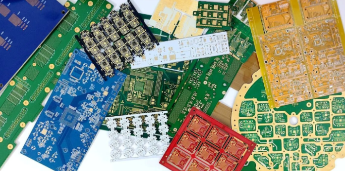
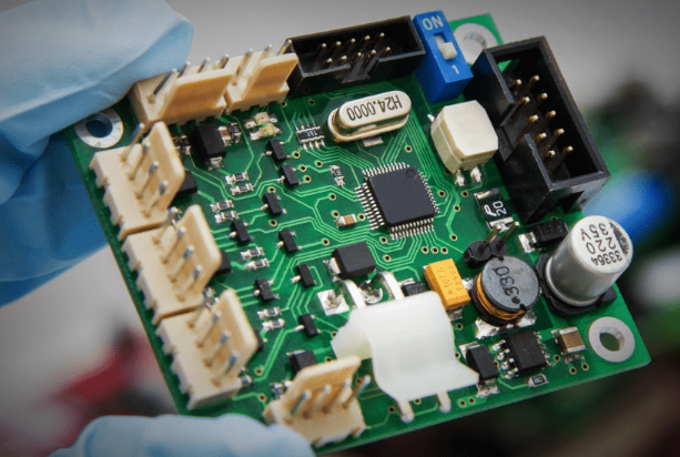
Gold recovery from electronics requires controlled processing, chemical knowledge, and strict safety discipline. Gold on printed circuit boards exists only as a thin surface layer used for conductivity and corrosion resistance. Extracting it involves mechanical separation followed by chemical dissolution and refining. Uncontrolled or improvised methods are hazardous and environmentally unsafe.
This guide explains how to remove gold from a circuit board, where gold is located, which industrial methods are used, and why high-reliability industries depend on gold plating in the first place.
How To Remove Gold From A Circuit Board Safely And Effectively?
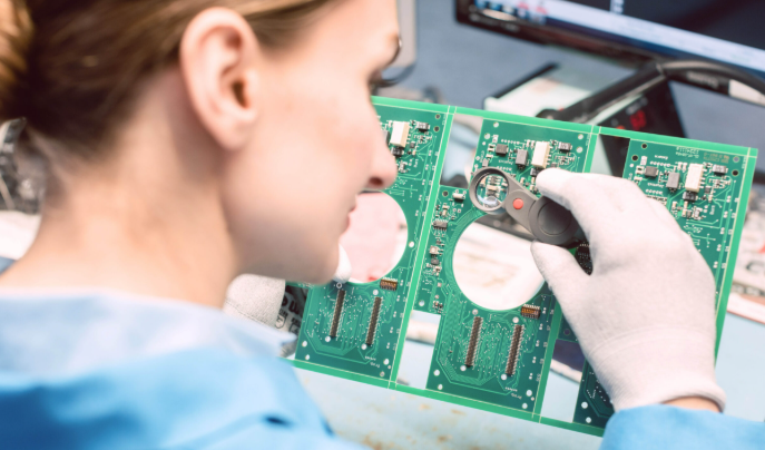
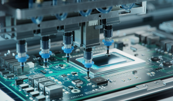
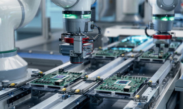
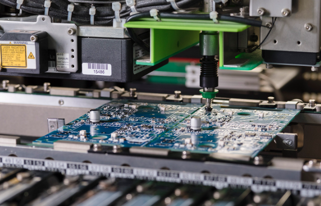
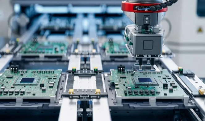
Gold removal is performed through staged processing: identification, mechanical preparation, chemical leaching, and metal precipitation. Industrial recyclers use controlled laboratory environments with ventilation, waste treatment, and chemical handling systems.
Step 1 – Identify Gold-Bearing Areas
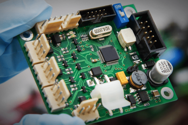
Gold is not embedded throughout the board substrate. It appears only in specific conductive areas:
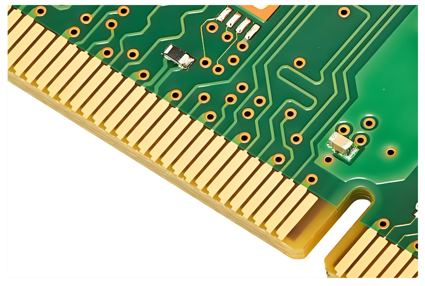
- Edge connectors (gold fingers)
- High-reliability connector pads
- BGA bonding pads
- CPU socket contacts
- Relay contact surfaces
Gold plating thickness is extremely thin, typically measured in microns or less.
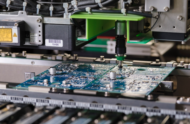
Step 2 – Mechanical Pre-Processing
Before chemical extraction, components must be removed and gold-bearing sections isolated.
Professional processes include:
- Depopulating components using controlled heat systems
- Cutting gold finger edges
- Shredding boards for chemical exposure (industrial scale only)
This stage increases chemical efficiency during dissolution.
Step 3 – Chemical Leaching Methods
Gold is chemically dissolved using controlled reagents. The process requires precision and industrial compliance.
| Method | Chemicals Used | Technical Control Required | Industrial Application |
| Aqua Regia | Nitric + Hydrochloric Acid | High precision | Laboratory refining |
| Cyanide Leaching | Sodium cyanide | Strict regulation | Industrial mining |
| Reverse Electroplating | Acid electrolyte + DC current | Controlled current density | Professional recycling |
| Thiourea Method | Acidic thiourea solution | Alternative chemistry | Limited industrial use |
All methods require fume extraction, chemical neutralization, and waste treatment.
Step 4 – Gold Precipitation And Refining
After dissolution:
- A reducing agent precipitates gold particles
- The precipitate is filtered and washed
- The material is dried and smelted
Industrial refining achieves purity above 99.9%.
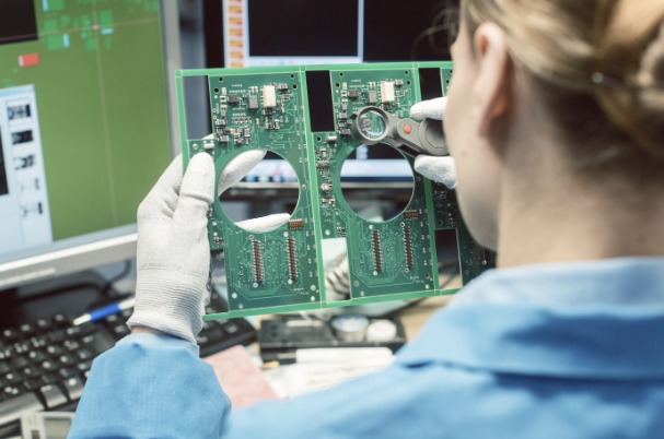
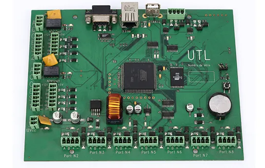
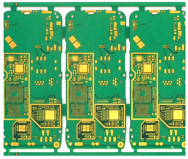
Where Is Gold Located on a Circuit Board?
Gold appears only in surface-finished contact areas designed for conductivity stability and oxidation resistance.
Common locations include:
- Gold fingers (edge connectors)
- ENIG pads
- ENEPIG wire bonding areas
- Aerospace-grade connectors
- High-end telecom backplane contacts
How Much Gold Is on a Circuit Board?
The quantity is extremely small, most consumer boards contain only milligrams of gold.
| Device Type | Typical Gold Content |
| Smartphone PCB | 0.02g – 0.05g |
| Computer motherboard | 0.2g – 0.5g |
| Industrial telecom board | Slightly higher |
| High-reliability board | Depends on connector density |
ENIG gold thickness is typically 0.05–0.1 microns. Large volumes are required for meaningful recovery.
Is It Legal To Remove Gold From Circuit Boards?
Regulations vary by country and region. Chemical processing involving acids or cyanide is typically restricted to licensed facilities.
Key compliance areas include:
- Hazardous waste disposal
- Toxic gas management
- Chemical transportation laws
- Wastewater neutralization
Unauthorized chemical recovery may violate environmental regulations.
What Is The Safest Industrial Method To Extract Gold?
Reverse electroplating under laboratory control reduces toxic gas generation compared to acid dissolution alone.
Industrial systems include:
- Controlled current supply
- Ventilated enclosures
- Acid-resistant containment
- Waste neutralization systems
Can Gold Be Removed Without Chemicals?
Yes, mechanical removal can collect gold-plated connectors, but it does not extract gold in metallic form. Scraping or sanding only removes thin plating. Refining still requires chemical processing.
What Is ENIG And Does It Contain Gold?
ENIG stands for Electroless Nickel Immersion Gold. It is a surface finish used in PCB manufacturing.
Layer structure:
- Copper base
- Nickel barrier layer
- Thin immersion gold coating
The gold layer protects the nickel and ensures solderability and oxidation resistance.
What Environmental Risks Are Associated With Gold Recovery?
Improper chemical recovery creates serious hazards:
- Nitrogen dioxide gas release
- Acid burns
- Heavy metal wastewater contamination
- Fire and chemical reaction risks
Professional recycling facilities operate with closed-loop systems to mitigate these risks.
How Do Professional PCB Manufacturers Control Gold Usage?
Gold is applied selectively to reduce waste while maintaining reliability.
Engineering practices include:
- Hard gold on connector surfaces
- ENIG for solder pads
- ENEPIG for wire bonding
- Thickness control per IPC standards
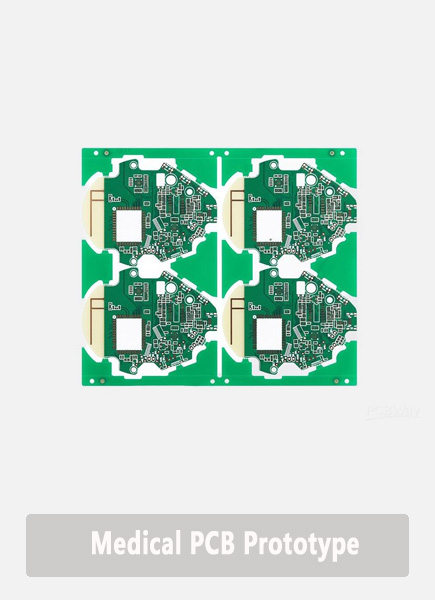
Medical, aerospace, and industrial boards use controlled plating thickness to balance performance and material efficiency.
FAQs
1. Can I burn circuit boards to extract gold?
Burning releases toxic fumes and does not isolate gold effectively. It is unsafe and environmentally damaging.
2. Does nitric acid alone dissolve gold?
Nitric acid dissolves base metals but does not dissolve gold independently.
3. How long does aqua regia take to dissolve gold?
Under controlled temperature and concentration, dissolution may take several hours. Process control is critical.
4. Do all PCBs contain gold?
No. Many consumer boards use HASL or OSP finishes and contain no gold plating.
5. Is small-scale gold recovery practical?
Due to extremely thin plating, small-scale recovery rarely produces meaningful yield.