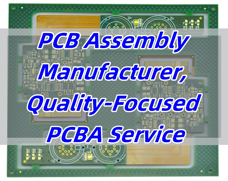
PCB design for manufacturing plays a crucial role in ensuring that circuit boards are not only functional but also cost-effective and easy to produce. A well-designed PCB minimizes production challenges, reduces material waste, and enhances reliability. Whether you’re developing simple single-layer boards or complex multilayer PCBs, applying design for manufacturing (DFM) principles can make a significant difference. In this guide, we’ll explore everything you need to know about PCB design for manufacturing, from material selection to industry applications and best practices for efficient production.
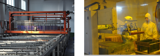
EBest Circuit (Best Technology) has over 18 years of experience in PCB design & manufacturing services. Since 2006, EBest Circuit (Best Technology) has continued to provide various high-quality printed circuit boards for telecommunication, wearable products, control & security systems, power supply, mobile phones, LEDs, and others. EBest Circuit (Best Technology) is to be the most reliable one-stop fast solution provider of electronics and circuit boards in the world, which is our company vision. If you have questions or inquiries about PCB design for manufacturing, just let us know via sales@bestpcbs.com.
What is PCB Design for Manufacturing?
PCB design for manufacturing focuses on creating circuit boards that are easy to produce while maintaining high quality. This process ensures fewer errors, lower costs, and faster production. By following design for manufacturing (DFM) principles, engineers prevent issues that may arise during fabrication, assembly, and testing.
What Material Will Be Used for PCB Design for Manufacturing?
Material selection plays a vital role in PCB performance. The common options include:
- FR4 – A cost-effective, widely used material with good insulation properties.
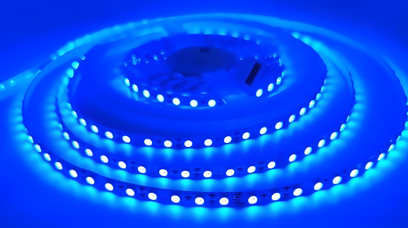
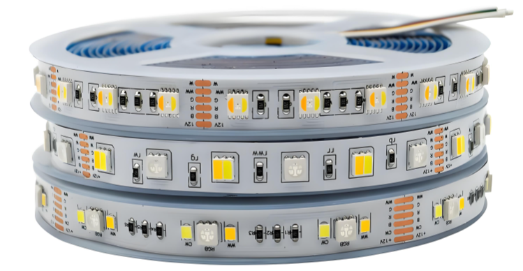
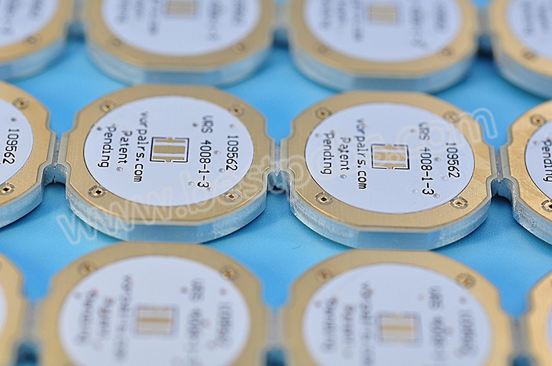
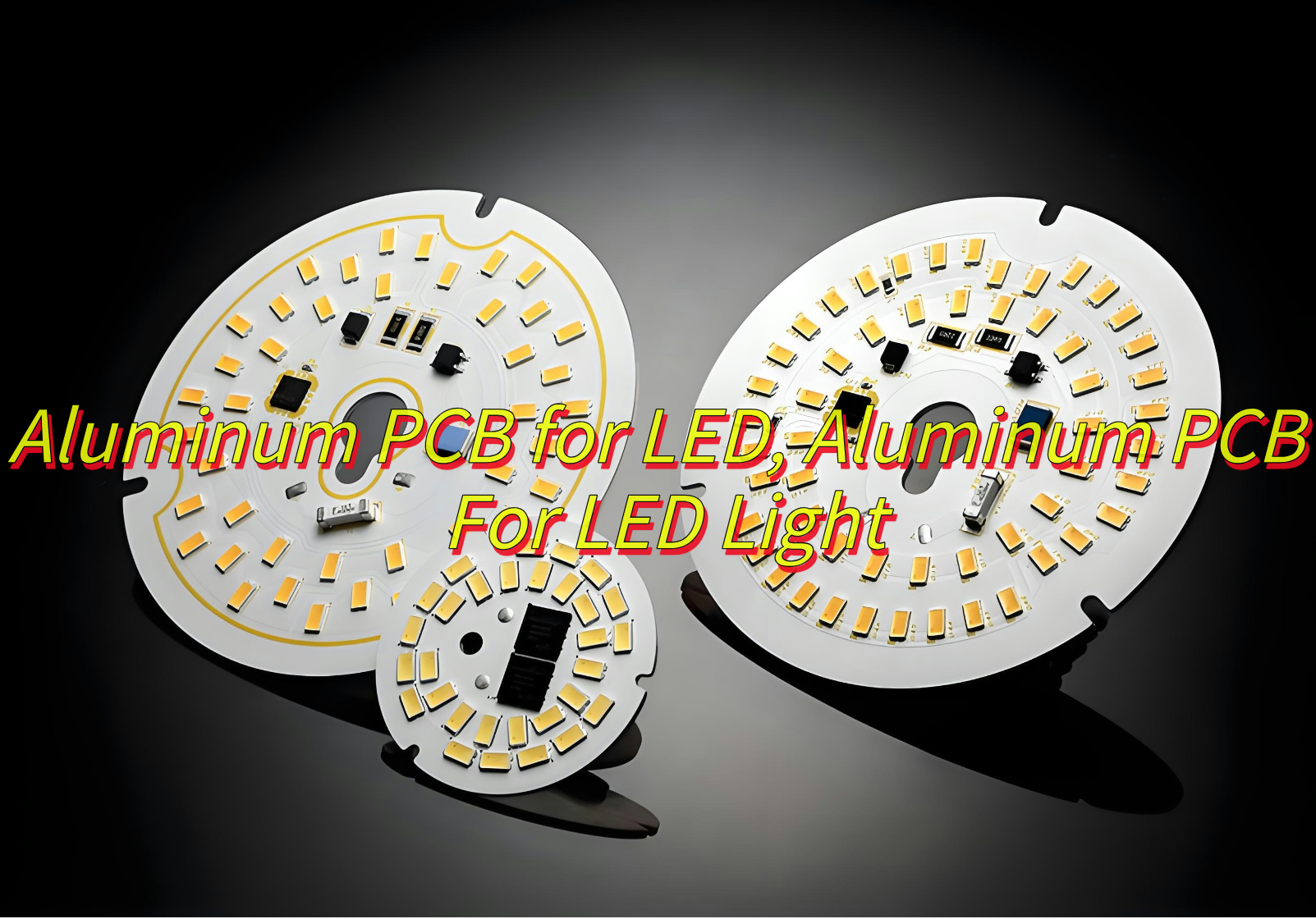
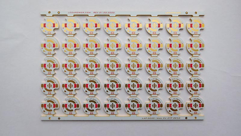
- Metal Core – Ideal for high-power applications requiring heat dissipation.
- Polyimide – Preferred for flexible and high-temperature applications.
- Rogers Material – Used in high-frequency PCBs where signal integrity is critical.
Choosing the right material impacts durability, thermal management, and overall functionality.
Are There Different Types of PCB Designs for Manufacturing?
Yes, PCB designs vary based on application and complexity. Some common types include:
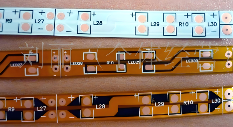
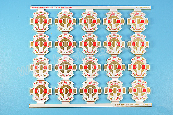
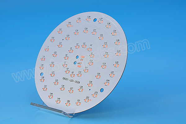
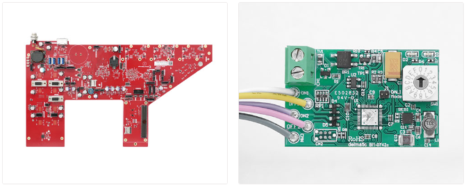
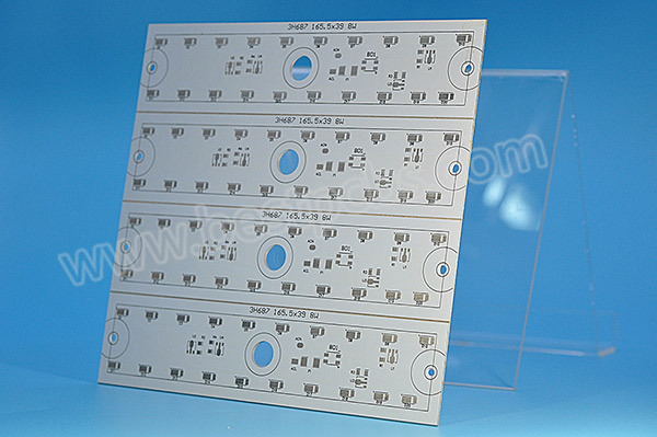
- Single-layer PCBs – Simple and cost-effective, used in low-power applications.
- Double-layer PCBs – Offer more routing flexibility and higher component density.
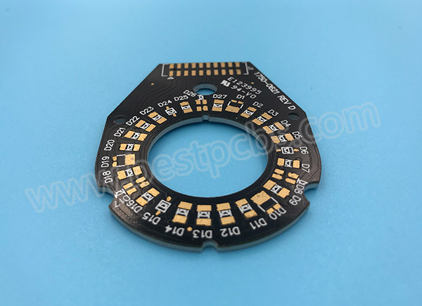
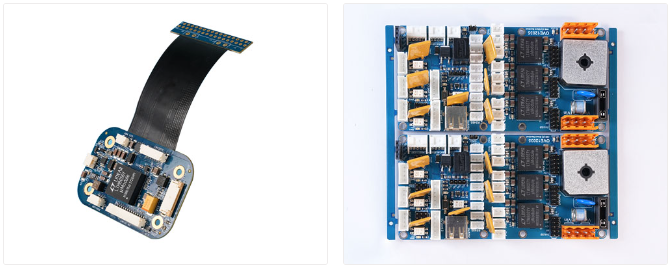
- Multilayer PCBs – Used in complex electronics like medical devices and aerospace systems.
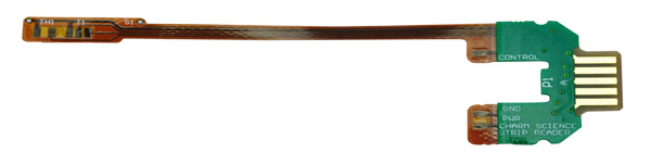
- Rigid-flex PCBs – Combine flexibility and rigidity for compact electronic products.
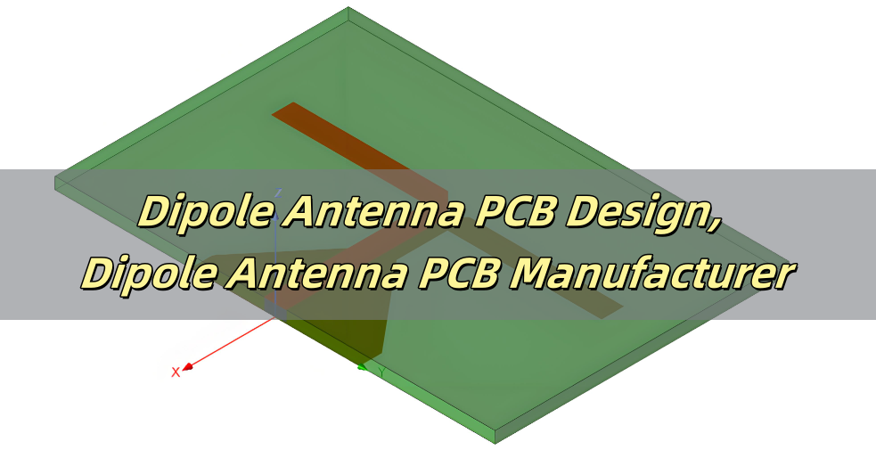
- High-frequency PCBs – Designed for fast signal transmission with minimal interference.
Understanding these types helps in selecting the best design for specific requirements.
What Are the Benefits of PCB Design for Manufacturing?
A well-optimized design offers multiple advantages:
- Lower production costs – Reducing design errors minimizes rework and material wastage.
- Improved reliability – Well-planned layouts ensure better performance and longevity.
- Faster production – Streamlined designs lead to shorter fabrication and assembly times.
- Better thermal management – Selecting the right material prevents overheating.
- Higher yield rates – Fewer design flaws increase the number of functional boards per batch.
- Enhanced manufacturability – Simplifying layouts and optimizing trace routing make production smoother.
- Reduced time-to-market – A properly designed PCB speeds up the entire production cycle.
Implementing DFM principles results in cost-effective and high-quality PCBs.
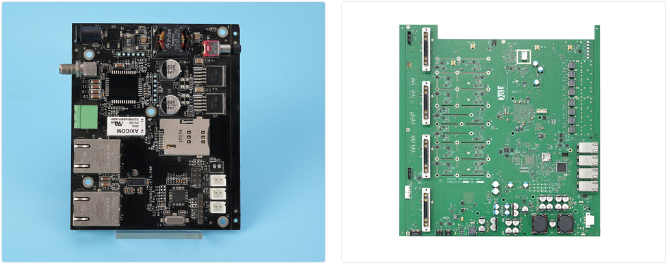
What Are the Applications of PCB Design for Manufacturing?
PCBs are essential in many industries. Common applications include:
- Consumer Electronics – Smartphones, laptops, and wearable devices.
- Automotive – Engine control units, infotainment systems, and sensors.
- Medical Devices – Diagnostic equipment and patient monitoring systems.
- Aerospace and Defense – Radar, communication systems, and navigation equipment.
- Industrial Automation – Robotics, power supplies, and control systems.
- Telecommunications – High-speed networking equipment and wireless communication systems.
Each sector requires specific design considerations to meet performance and safety standards.
Why Should You Choose EBest Circuit (Best Technology) as Your PCB Design Partner?
- Strong R&D Team, Know How-To: EBest Circuit (Best Technology) has a strong R&D team and engineers with more than 10 years of experience, and excellent management personnel, which give us access to optimize the PCB design and manufacturing process and minimize product costs to customers. The manager of the engineering department has accumulated about 17 years of experience. He is proficient in engineering design, cost estimation, and systematic PCB knowledge, with extensive team management experience. The director of the quality department has over 10 years of experience in PCB engineering design, with a background in engineering EQ(Engineering Query) and customer complaint handling, and extensive expertise in the PCB industry.
- One-stop Service (PCB+BOM+Assembly): Our services cover the entire process, from assembly and component sourcing to seamless technical support at every stage of your project—ensuring expert guidance from initial planning through post-sales implementation.
- Quick Turn-out, On-time Delivery: EBest Circuit (Best Technology) now offers a rapid 2-3 week delivery timeframe to help customers accelerate product launches and reduce time-to-market.
- High Quality, Special Request Available: We are dedicated to providing high quality, service and value to our customers while maintaining our traditional dedication to excellence. Apart from the normal PCB, we also customized the PCB products according to our customers’ requests, such as some highly difficult non-standard, complicated PCB projects.
How to Do PCB Design and Manufacturing?
A structured PCB design and manufacturing process ensures successful PCB production:
Step 1: Design Layout and Schematic Creation
- Engineers design the circuit using PCB design software, ensuring proper component placement and routing.
Step 2: Design Rule Check (DRC) and DFM Analysis
- Running a DRC and DFM analysis prevents potential manufacturing issues early in the process.
Step 3: Generating Gerber Files
- Gerber files contain all the information needed for PCB fabrication, including copper layers, drill files, and solder masks.
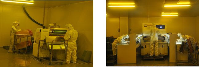
Step 4: PCB Fabrication Process
The PCB manufacturing process follows these steps:
- Material Preparation – Cutting and preparing the base material.
- Circuit Patterning – Applying the circuit layout using etching or additive processes.
- Drilling – Creating holes for vias and components.
- Plating and Solder Mask Application – Enhancing conductivity and protecting the board.
- Silkscreen Printing – Adding component labels and markings.
- Final Inspection and Testing – Ensuring the board meets specifications.
Step 5: PCB Assembly
- After fabrication, components are soldered onto the board using SMT or through-hole assembly.
Step 6: Testing and Quality Assurance
- Each PCB undergoes electrical testing, visual inspection, and functional tests to verify performance.
Step 7: Final Delivery
- Once approved, the finished PCBs are packed and shipped to customers.
In conclusion, PCB design for manufacturing enhances production efficiency, reduces costs, and improves reliability. Choosing the right materials and design principles ensures better performance across industries. EBest Circuit (Best Technology) provides expert support, advanced DFM analysis, and high-quality PCB manufacturing to meet diverse needs. Whether you need quick prototypes or large-scale production, we ensure smooth execution. If any new inquiries about PCB design & manufacturing services, feel free to let us know at sales@bestpcbs.com. It’s our pleasure to cooperate with you about any PCB projects to get a win-win situation.