If you’re looking for a reliable humidifier PCB manufacturer, EBest is your first choice—we specialize in solving the most frustrating pain points of humidifier PCB design, prototype, and assembly. Our custom solutions meet industry standards and unique project needs, with engineering expertise to turn concepts into high-performance, durable humidifier PCB products.
What Are Common Questions About Humidifier PCB?
Common questions about humidifier PCB revolve around performance, compliance, and practical application. Key queries include fixing EMC radiation issues, preventing moisture-induced failures, and securing fast, accurate prototypes.
Below, we answer these humidifier PCB questions in detail. Each response includes technical solutions and real-world case studies to back our expertise and authority.
How Does EBest Solve Humidifier PCB Design Challenges?
What Are the Top Pain Points of Humidifier PCB Design?
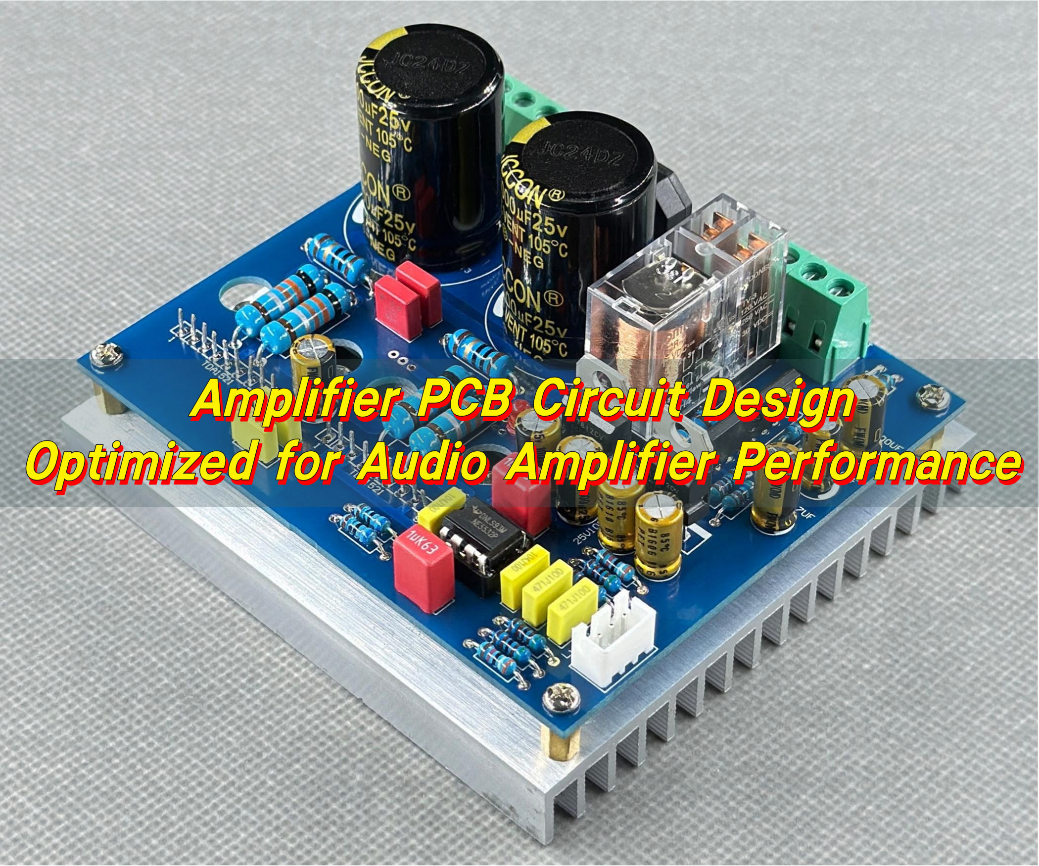
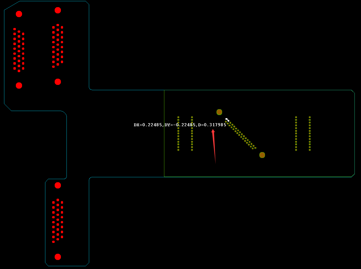
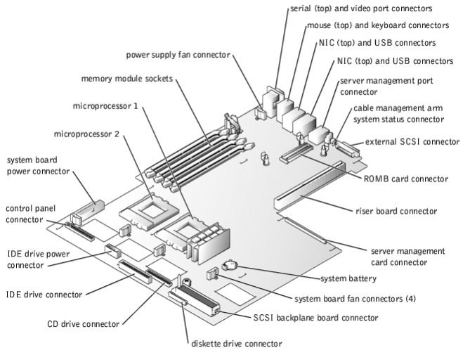
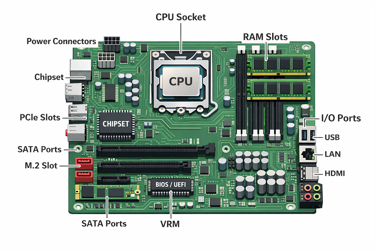
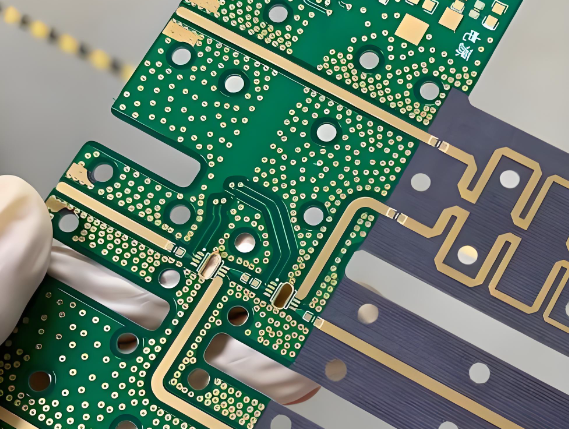
The biggest challenges in humidifier PCB design include EMC compliance (EN 61000-6-3:2021), moisture resistance, limited space for portable models, and high-frequency component interference.
Engineers often struggle with radiation excess, grounding loop issues, and balancing performance with compact design—problems that delay production and increase rework for humidifier PCB projects.
How Does EBest Solve Humidifier PCB Design Challenges?
Our engineering team uses a data-driven approach to eliminate humidifier PCB design pain points, with industry-tailored solutions:
- EMC Compliance: Meet EN 61000-6-3:2021 with “three-zone independent grounding + single-point convergence” topology, reducing radiation by 30-40% and lowering impedance to ≤2Ω at 200MHz.
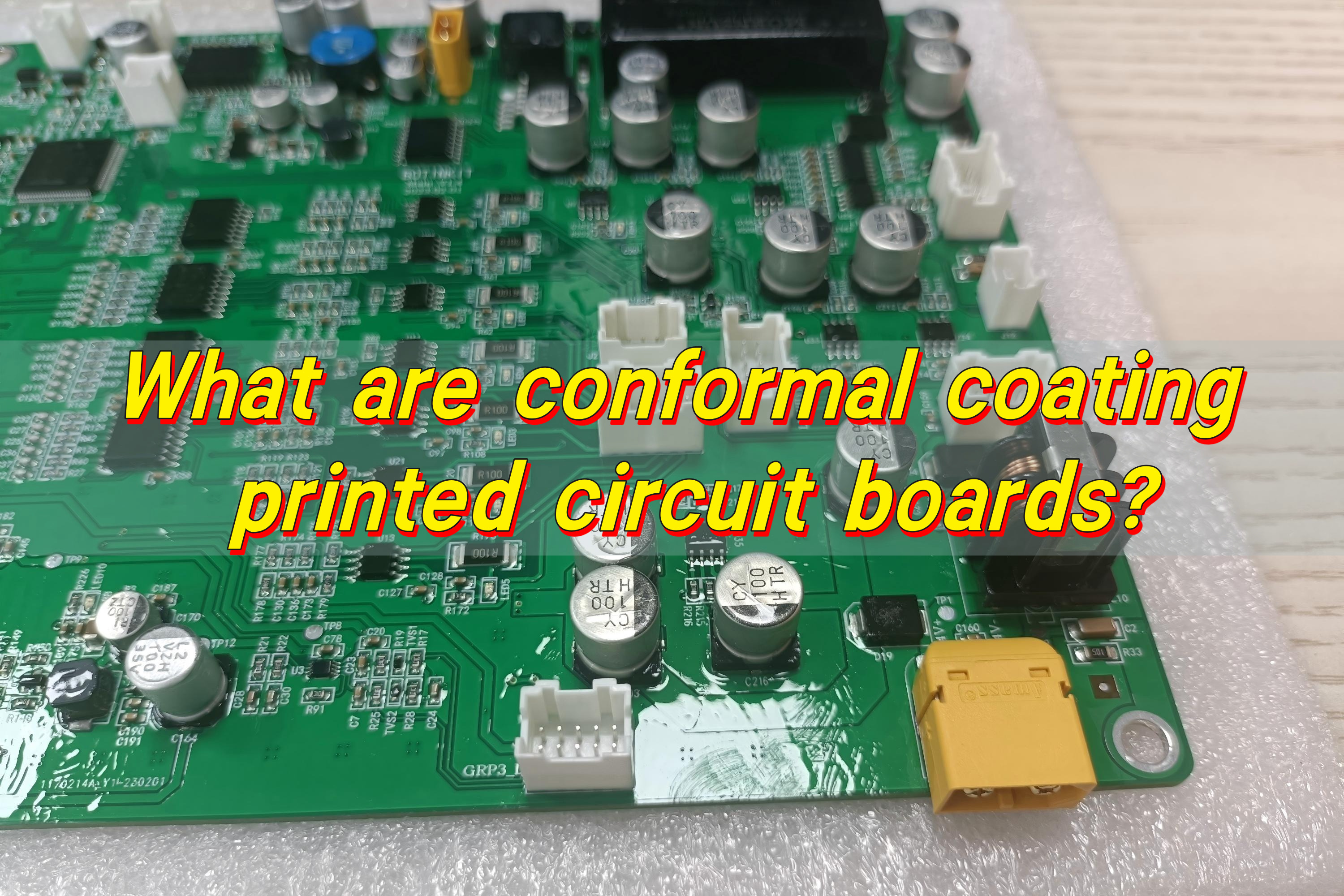
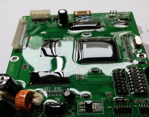
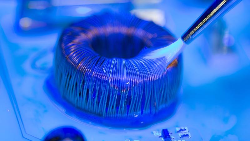
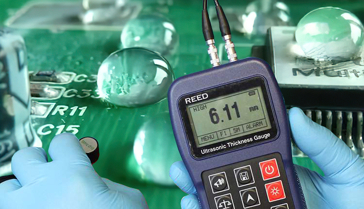
- Moisture Resistance: Use low-hygroscopicity FR-4 substrates and conformal coatings; add water-resistant barriers for high-humidity use (e.g., medical humidifier PCB).
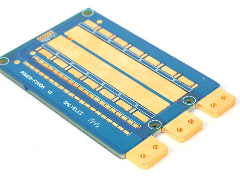
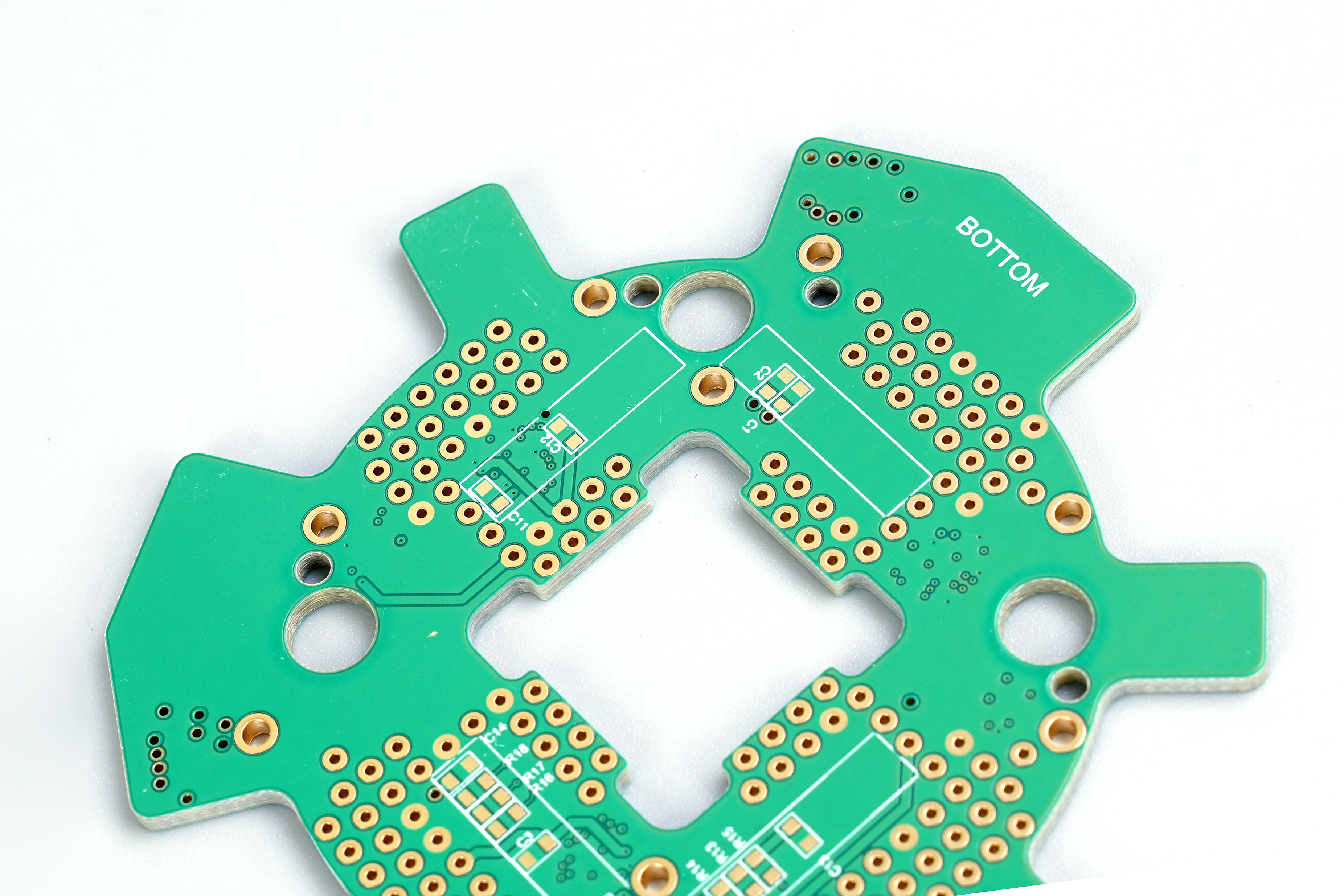
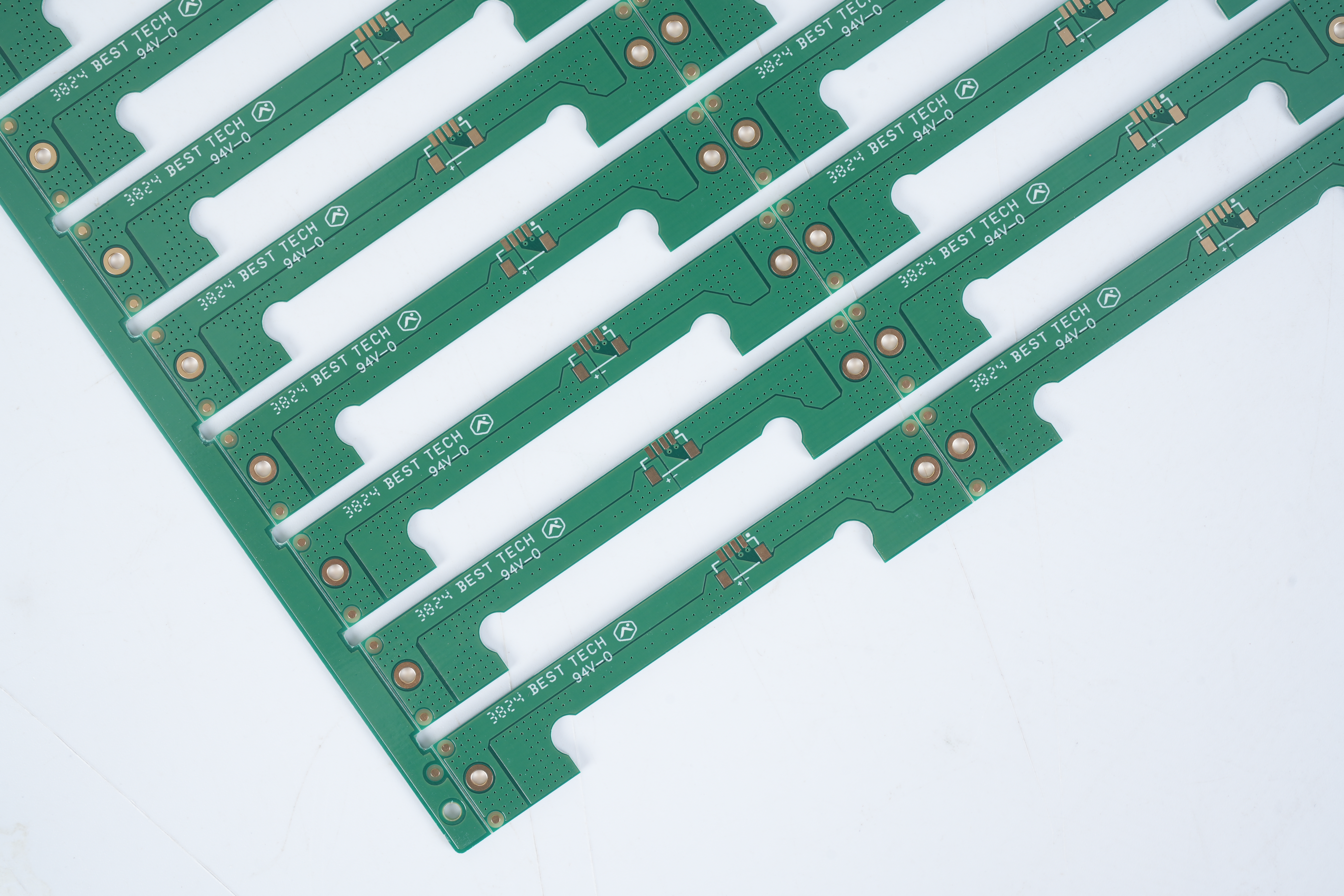
- Space Optimization: For portable humidifier PCB (≤40mm×60mm), use dense component placement, narrow durable traces (≥0.2mm), and integrated functions.
- Component Interference: Separate ultrasonic atomization drivers from sensitive circuits by ≥8mm, use shielding copper rings, and avoid right-angle bends (reducing radiation leakage by 5-10dB).
For reliable, compliant humidifier PCB design, choose EBest. Our custom solutions match your exact specs, with engineering support from concept to production.
How Does EBest Solve Humidifier PCB Prototype Challenges?
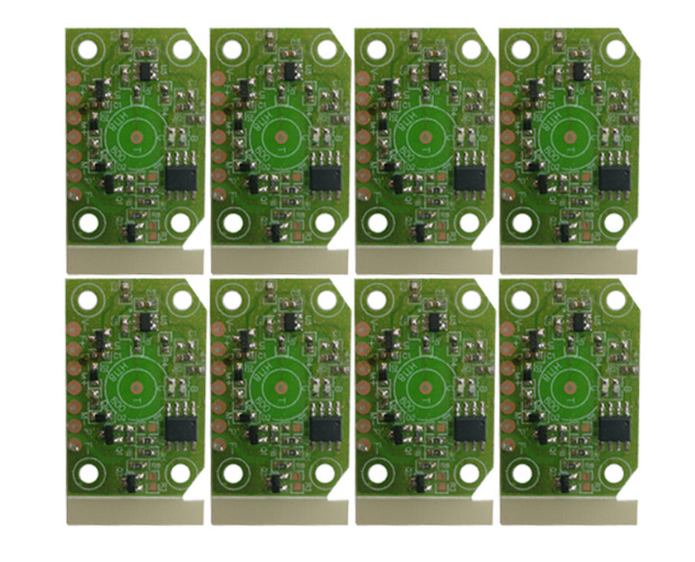
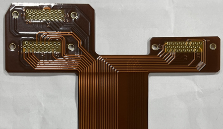
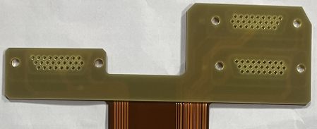
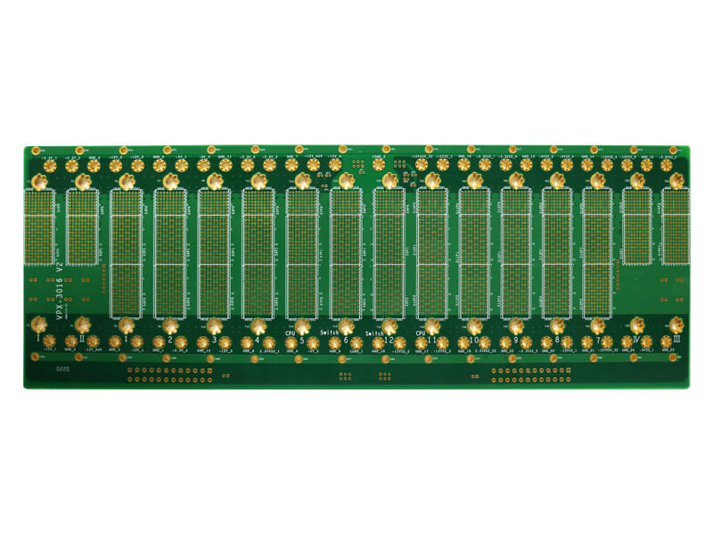
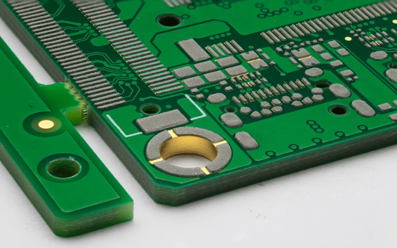
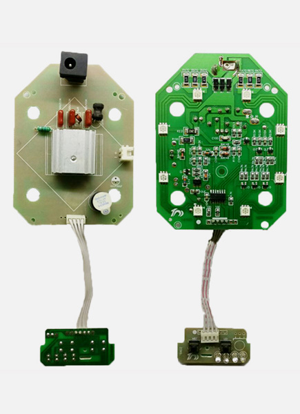
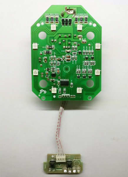
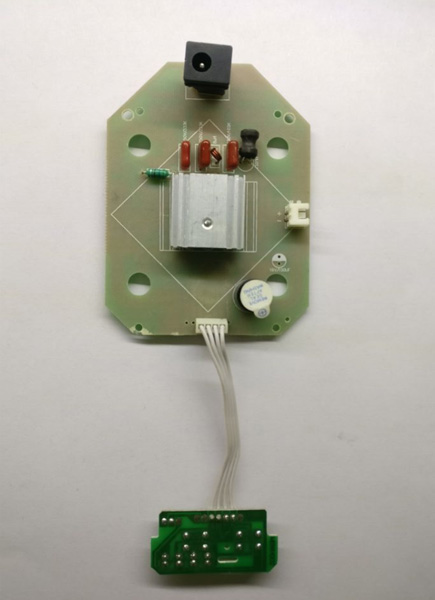
Humidifier PCB Prototype
What Are the Main Pain Points of Humidifier PCB Prototype?
Engineers face two key humidifier PCB prototype challenges: slow turnaround times (delaying testing) and inconsistency (prototypes failing to match design specs).
Other pain points include poor solder quality, incorrect component placement, and lack of critical testing (EMC, moisture resistance) for humidifier PCB prototype.
How Does EBest Solve Humidifier PCB Prototype Challenges?
We streamline the humidifier PCB prototype process for fast, accurate, reliable samples, with zero quality compromise:
- Fast Turnaround: Same-day production for simple humidifier PCB prototype; 2-3 day turnaround for complex multi-layer designs.
- Consistency & Accuracy: Use automated fabrication and AOI testing to ensure prototypes match design files exactly; verify placement, solder joints, and trace integrity.
- Pre-Production Testing: Every humidifier PCB prototype undergoes EMC (30MHz-6GHz), moisture resistance, and functional testing (atomization control, fan speed).
- Engineering Support: Get feedback on prototype performance and design tweaks to improve humidifier PCB reliability before assembly.
Need fast, reliable humidifier PCB prototype? EBest’s service is tailored to your needs—contact us to get started.
How Does EBest Solve Humidifier PCB Assembly Challenges?
What Are the Top Pain Points of Humidifier PCB Assembly?
Humidifier PCB assembly challenges focus on quality control, component compatibility, and specialized requirement adaptability.
Common pain points include poor solder joint reliability, flux/debris contamination, compact assembly difficulty, and failure to meet industry cleanliness standards.
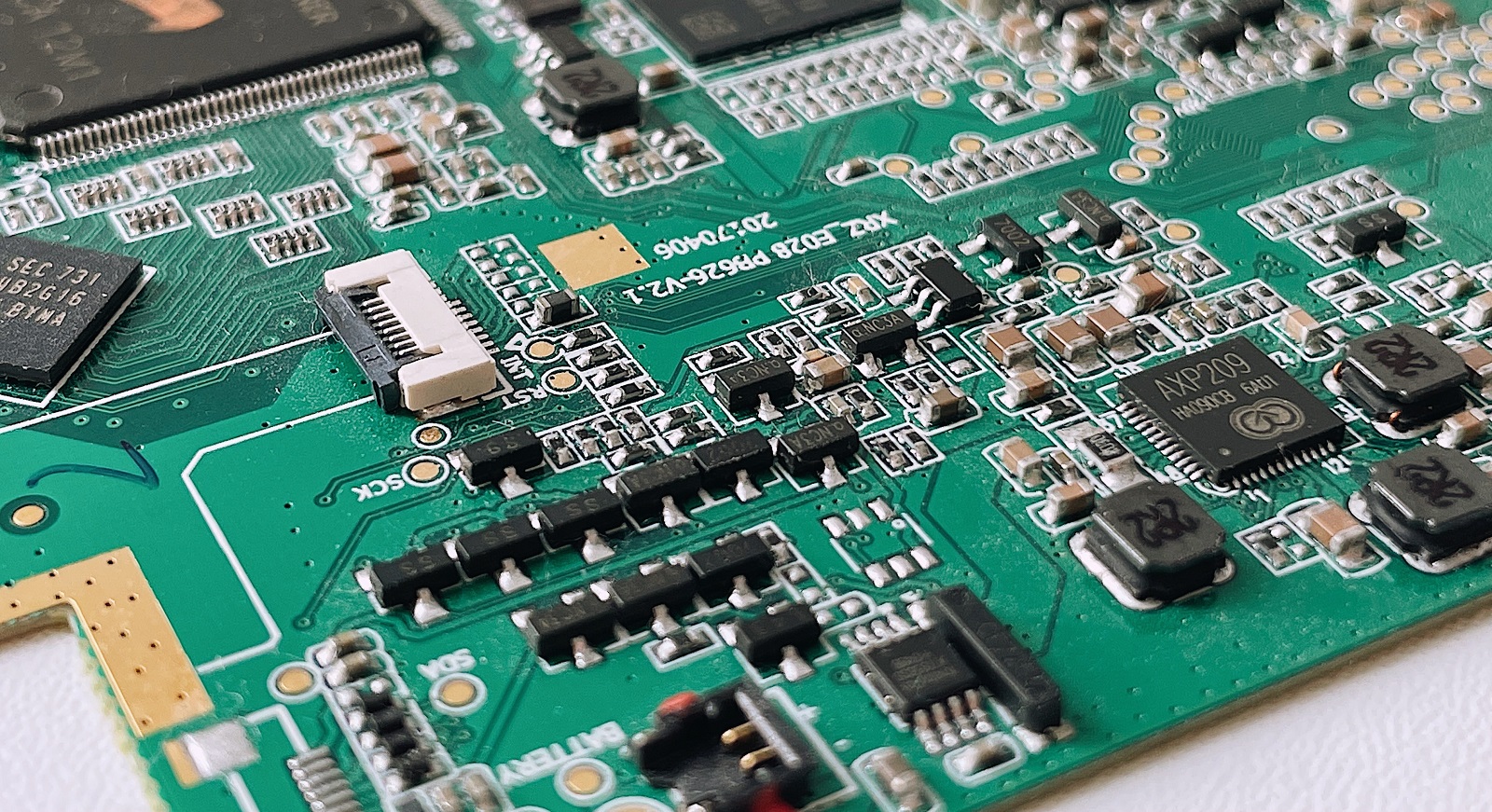
Humidifier PCB Assembly: Pain Points, Challenges & Our Solutions
Our humidifier PCB assembly process combines advanced technology, strict QC, and industry expertise for flawless results:
- Solder Quality: Automated SMT assembly and reflow soldering (±1℃ precision); post-assembly X-ray and visual inspection to eliminate cold solder/bridging.
- Contamination Control: No-clean flux and ultrasonic cleaning for medical/aerospace humidifier PCB assembly; ionic testing to prevent moisture-induced corrosion.
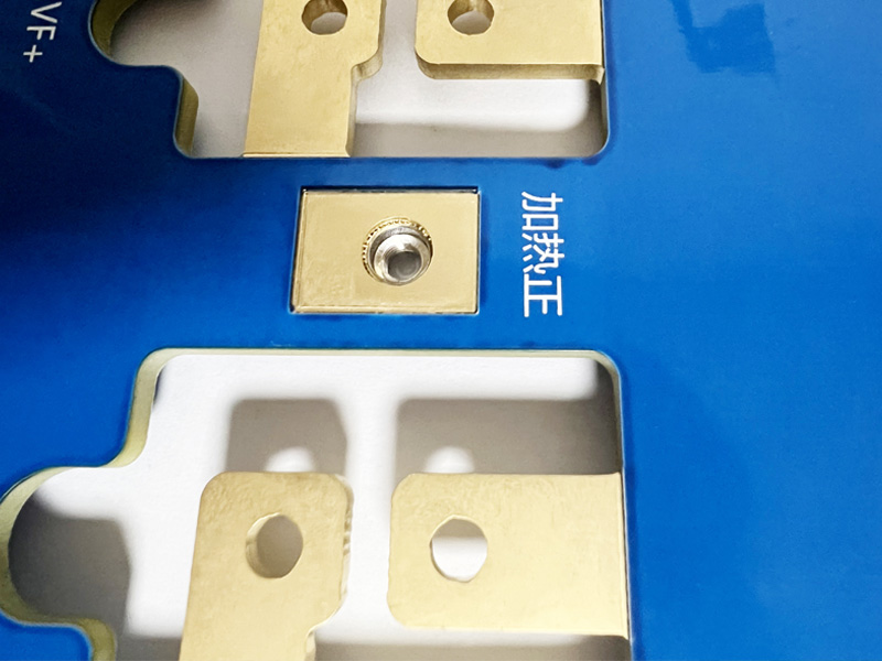
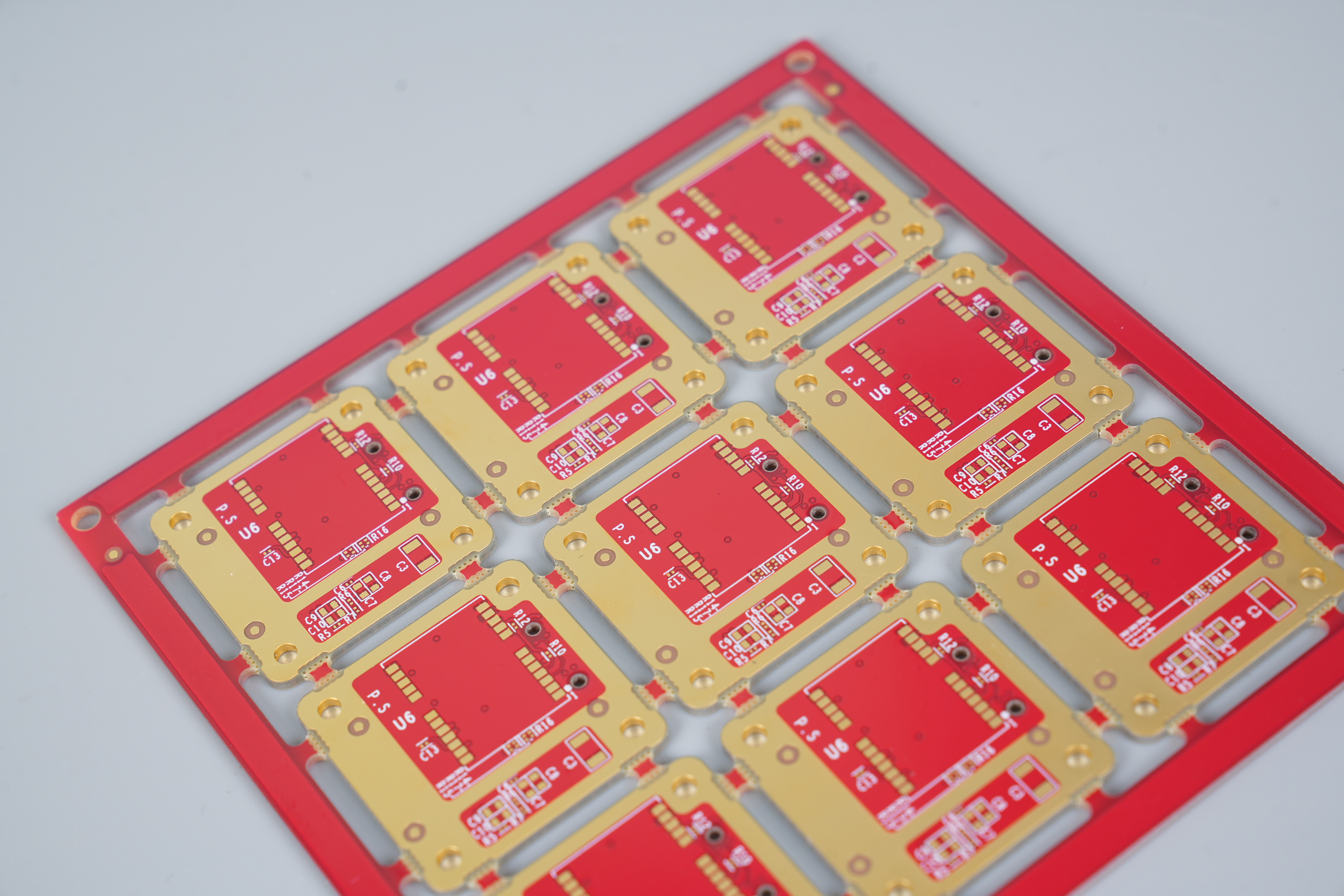
- Compact Assembly: Specialize in small-form-factor humidifier PCB (≤40mm×60mm) with precision placement (±0.03mm accuracy) for tiny components (0402 size).
- Industry Compliance: Tailor processes—anti-static materials for industrial use; traceability systems for medical humidifier PCB assembly.
For high-quality humidifier PCB assembly, trust EBest. Our service is fast, reliable, and customized to your project.
Humidifier PCB Industry Case Studies (Medical, Aerospace, Industrial)
Medical Humidifier PCB Case Study
A leading medical device manufacturer needed a medical humidifier PCB for a portable respiratory humidifier (ISO 13485 compliance, moisture resistance, low power).
Their previous supplier struggled with radiation excess and moisture failures; EBest’s custom medical humidifier PCB met EN 61000-6-3:2021, with zero field failures in the first year.
Aerospace Humidifier PCB Case Study
An aerospace company required an aerospace humidifier PCB for aircraft cabin environmental control (RTCA DO-160 compliance, -40℃ to 85℃ resistance).
We used high-temperature FR-4 substrates and military-grade components; the aerospace humidifier PCB passed all DO-160 tests and is integrated into commercial aircraft worldwide.
Industrial Humidifier PCB Case Study
An electronic factory humidifier manufacturer needed a humidifier PCB (±1% RH precision, ≤50V anti-ESD) to fix inconsistent performance.
EBest’s custom humidifier PCB reduced humidity fluctuations by 80% and cut production defects from 8% to 1.2%.
Why Choose EBest for Your Humidifier PCB Needs?
EBest stands out for humidifier PCB design, prototype, and assembly—backed by engineering expertise and industry experience:
- Technical Expertise: Our engineers specialize in humidifier PCB solutions, solving complex pain points other manufacturers can’t.
- Custom Solutions: Every humidifier PCB is tailored to your specs (compact portable designs to rugged aerospace humidifier PCB models).
- Strict Quality Control: ISO 9001/13485 compliance, with 100% testing (AOI, X-ray, EMC, moisture) at every stage.
- Fast Delivery: Prioritize humidifier PCB projects, with 2-3 day prototype turnaround and efficient assembly lead times.
FAQ: Common Humidifier PCB Questions & Solutions
1. How to Fix EMC Radiation Overruns in Humidifier PCBs?
EMC radiation overruns in humidifier PCBs stem from atomization module emissions, poor grounding, or component interference. Use “three-zone independent grounding + single-point convergence” topology.
Add high-frequency filters, separate atomization modules by ≥8mm, and use multi-via grounding (4+ vias) to cut radiation by 30-40%.
2. What Materials Prevent Moisture-Induced Humidifier PCB Failures?
Use low-hygroscopicity FR-4 substrates and conformal coatings (e.g., Parylene) to seal the moisture resistant humidifier PCB and prevent corrosion/dielectric breakdown.
For medical/aerospace use, add water-resistant barriers and test in benchtop humidity chambers; avoid hygroscopic components.
3. How Long Does It Take to Get a Humidifier PCB Prototype?
EBest’s humidifier PCB prototype turnaround depends on complexity: same-day for simple single-layer designs, 2-3 days for complex multi-layer prototypes.
We prioritize speed without sacrificing accuracy, helping you test and iterate quickly on your humidifier PCB project.
4. Can Humidifier PCBs Be Customized for Medical Use?
Yes—EBest designs/assembles medical humidifier PCB fully compliant with ISO 13485 and EN 61000-6-3:2021 standards.
We use biocompatible materials, traceability systems, and strict contamination control for respiratory/neonatal humidifier applications.
5. Why Do Humidifier PCBs Fail During Assembly?
Humidifier PCB assembly failures come from poor solder joints, component contamination, or incorrect placement.
Use automated SMT assembly, no-clean flux, and post-assembly X-ray/visual inspection to avoid these issues.
6. How to Ensure Humidifier PCB Compatibility with Ultrasonic Atomization Modules?
Optimize humidifier PCB power delivery (stable 5V/3.3V) to the atomization driver and use a low-impedance grounding path.
Separate the driver from sensitive circuits, support 1.7-2.4MHz frequency, and add surge protection for the humidifier PCB.
Choose EBest for Your Humidifier PCB Projects
We provide high-quality humidifier PCB design, prototype, and assembly solutions, tailored to medical, aerospace, and industrial needs.
Our team solves humidifier PCB pain points, delivers fast turnaround, and ensures compliance. Contact us to place your order at sales@bestpcbs.com—EBest, your trusted humidifier PCB partner.