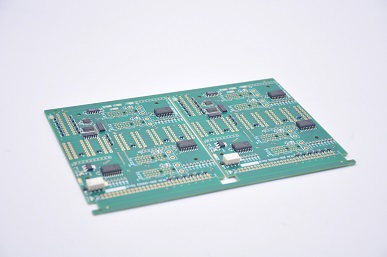
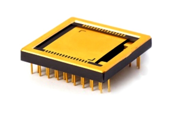
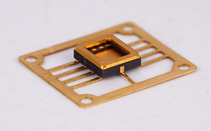
What Are RF Boards?
RF boards, or radio frequency printed circuit boards. RF boards are designed to operate with high-frequency signals, typically within the range of 3 kHz to 300 GHz. This capability makes them a critical component in devices that rely on wireless communication, such as mobile phones, satellite systems, and radar equipment.
Unlike regular FR4 PCBs, RF boards are optimized to handle electromagnetic waves in the radio frequency range. They use specialized materials and designs to minimize signal loss, avoid interference, and maintain stable operation. Their importance continues to grow with advancements in wireless technologies, the Internet of Things (IoT), and 5G networks.
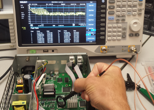
The design and manufacturing of RF boards demand meticulous attention to detail, as even minor issues can significantly impact their performance. These boards are vital for applications where precision and reliability are non-negotiable.
Advantages of RF Boards
- High-frequency systems require consistent and stable signal transmission. RF boards are designed to reduce signal distortion and ensure accuracy, even in complex environments.
- The specialized materials used in RF boards, such as PTFE and Rogers laminates, have low dielectric constants.
- RF boards are built to handle heat efficiently.
- RF boards can be tailored to meet specific requirements, including frequency range, size, and power capacity.
- With RF boards, engineers can integrate cutting-edge technologies like 5G, IoT, and advanced radar systems.
- RF boards design ensures long-term reliability, even under challenging conditions.
What Is the Difference Between RF PCB and Normal PCB?
While standard PCBs and RF PCBs may appear similar at first glance, their functions, materials, and design considerations set them apart.
- Frequency Handling
Standard PCBs are designed for low to medium frequencies and do not require the precision needed for high-frequency signals. RF PCBs, on the other hand, are built to handle frequencies ranging from kilohertz to gigahertz.
- Material Properties
Materials are a defining factor. Normal PCBs commonly use FR-4, a cost-effective and versatile material. In contrast, RF boards use materials like PTFE, Rogers laminates, or ceramic substrates. These materials have low dielectric constants and low loss tangents, ensuring minimal signal degradation.
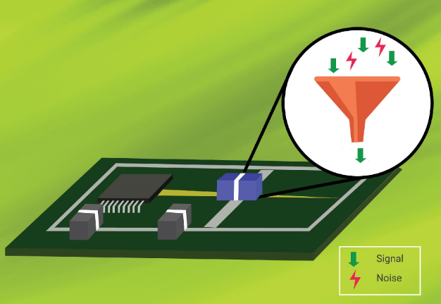
- Signal Integrity
RF boards are engineered to minimize crosstalk and interference. Design considerations include impedance matching and controlled trace dimensions, which are not as critical in standard PCBs.
- Application Areas
While standard PCBs are widely used in consumer electronics, RF PCBs find their place in specialized fields like telecommunications, aerospace, and medical devices, where high-frequency signals are essential.
Which Material Is Commonly Used for RF PCBs?
Material selection is critical when designing RF boards. The right material ensures that the board can handle high-frequency signals with minimal loss and distortion.
- PTFE (Polytetrafluoroethylene)
PTFE is a common choice for RF PCBs due to its excellent electrical properties. It has a low dielectric constant, which supports stable signal propagation. PTFE is also resistant to heat, making it suitable for high-power applications.
- Rogers Laminates
Rogers laminates are widely used in RF designs. These materials offer exceptional thermal stability and low loss tangents, ensuring reliable performance. They are also easy to process, making them a favorite among manufacturers.
- Ceramic-Filled Substrates
For applications requiring high power and thermal management, ceramic-filled substrates are an excellent option.
- Liquid Crystal Polymer (LCP)
LCP is a flexible, lightweight material suitable for RF boards used in compact devices like smartphones and wearables.
- Hybrid Materials
Some RF PCBs combine multiple materials to balance cost, performance, and manufacturability. Hybrid materials allow designers to meet specific application requirements effectively.
What Are RF Circuits Used For?
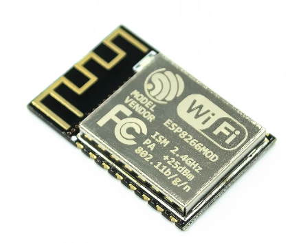
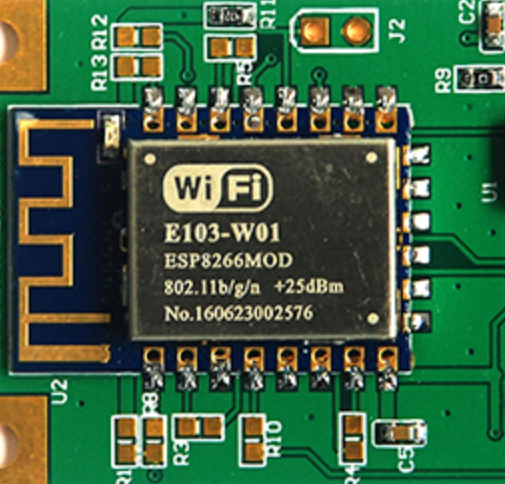
Telecommunication Systems – RF circuits are the backbone of mobile networks, Wi-Fi routers, and wireless communication devices.
Aerospace and Defense – Radar systems, satellite communication, and military-grade navigation rely on RF circuits.
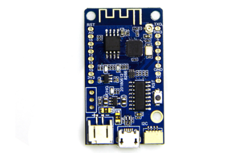
IoT Devices – The Internet of Things depends heavily on RF circuits for connectivity. From smart home systems to industrial sensors, these circuits enable real-time data exchange.
Medical Equipment – In healthcare, RF circuits support technologies like MRI machines and wireless patient monitoring systems.
Automotive Applications – RF circuits play a key role in modern vehicles, powering advanced driver-assistance systems (ADAS), vehicle-to-everything (V2X) communication, and keyless entry systems.
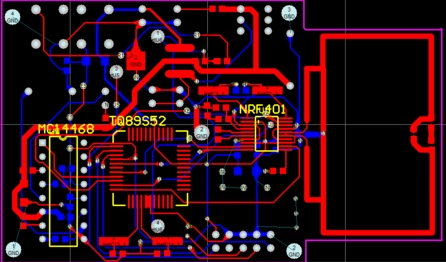
RF PCB Design Guidelines
Designing RF PCBs can be as challenging as addressing electromagnetic interference (EMI). Success often requires careful planning and attention to the following aspects:
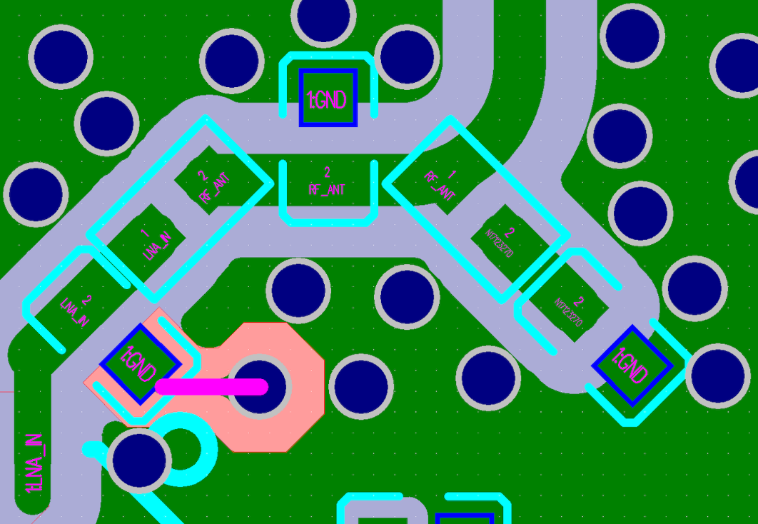
1. Transmission Lines
- Select the correct transmission line type (microstrip or stripline) based on the required 50Ω characteristic impedance.
- Use impedance calculation tools to design consistent impedance lines and determine appropriate line width and spacing.
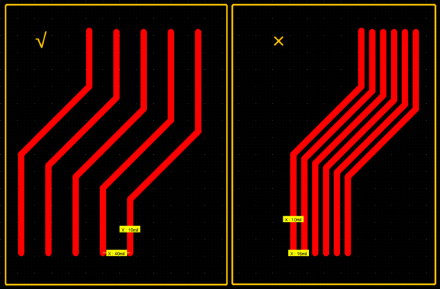
- Ensure continuity in RF transmission lines by maintaining uniform widths and spacing.
- Avoid abrupt transitions or splits in RF signal paths as they impact impedance.
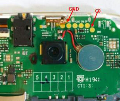
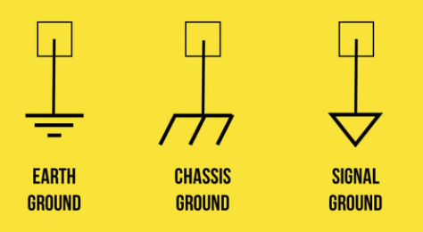
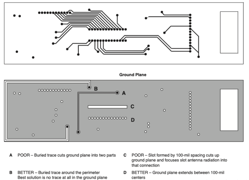
- Provide a clean ground reference under the transmission line without interference from other signals.
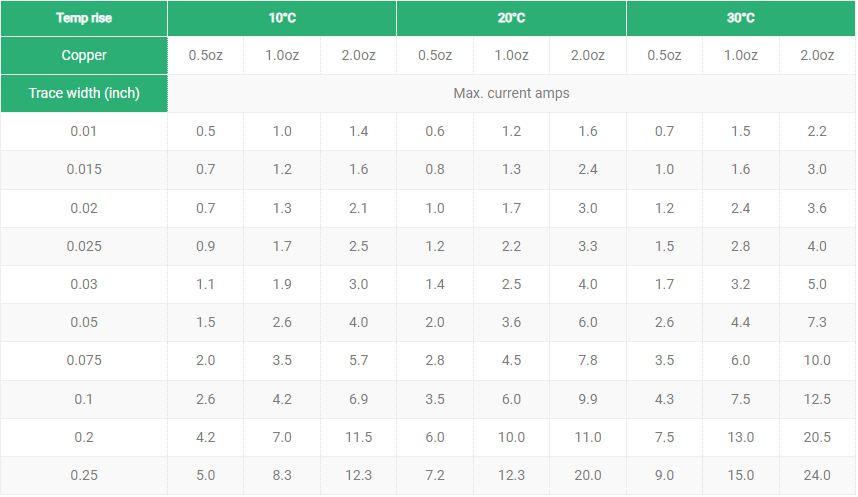
- Minimize transmission line lengths to reduce signal loss, and use wider traces for power lines.
- Use compensated bends for corners, avoiding sharp angles.
- Avoid forks, stubs, or parallel placement of other lines near RF transmission lines.
- Refrain from placing test points directly on RF transmission lines.
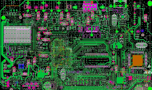
2. PCB Layer Stacking
- A recommended four-layer stackup for RF PCBs includes:
Top Layer: RF ICs, components, transmission lines, decoupling capacitors, and antennas.
Layer 2: Ground plane.
Layer 3: Power plane.
Bottom Layer: Non-RF components and signal traces.
- Ensure a complete and continuous ground plane for RF signal integrity.
- Follow the “20H rule,” where the power plane edges are recessed by at least 20 times the plane-to-plane spacing to reduce EMI.
3. Power Decoupling
- Place decoupling capacitors as close to power pins as possible.
- Use a combination of large and small capacitors for filtering different noise frequencies.
- Keep decoupling capacitors and power layers on the same plane, prioritizing smaller values near IC pins.
- Avoid vias between decoupling capacitors and IC power pins.
- Each decoupling capacitor should have a dedicated ground via.
4. Vias
- Use multiple vias to connect layers, spaced no greater than λ/20.
- Place ground vias near signal vias to minimize parasitics.
- Avoid sharing vias between solder pads and signal traces.
- Prefer smaller vias for reduced parasitic effects but balance against manufacturing costs.
- Employ ground vias around sensitive components to enhance EMC shielding.
5. Capacitors
- Use C0G/NP0 capacitors for temperature stability and frequency consistency.
- For decoupling, select capacitors with self-resonant frequencies (SRF) near the operational range.
- Employ smaller packages (e.g., 0201 or 0402) to minimize parasitic effects.
- Choose high-Q capacitors for RF circuits to reduce losses.
6. Inductors
- Use high-Q inductors operating below their SRF for matching circuits.
- For filtering, select inductors with SRF near the noise frequencies.
- Avoid parallel placement of adjacent inductors to prevent coupling.
- Wire-wound inductors offer low DC resistance, high Q, and better current handling, while ceramic inductors provide cost efficiency at the expense of lower Q.
At EBest Circuit (Best Technology), we specialize in manufacturing RF boards tailored to your specific needs. With a commitment to quality and innovation, we deliver solutions that meet the highest standards of performance and reliability. Contact us today to discuss how we can support your next project.