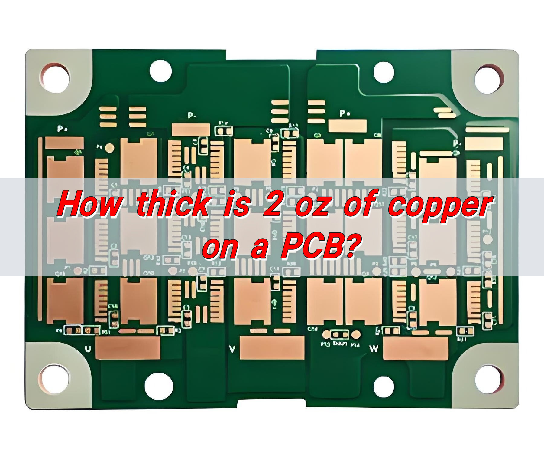
How thick is 2 oz of copper on a PCB? The thickness of 2 oz of copper on a PCB is about 70μm. Ounces are the common unit of PCB copper foil thickness. The thickness of 1 oz copper foil is generally about 35μm, so the thickness of 2 oz copper foil is about twice that of 1 oz, which is about 70μm.
How thick is the copper on a PCB board?
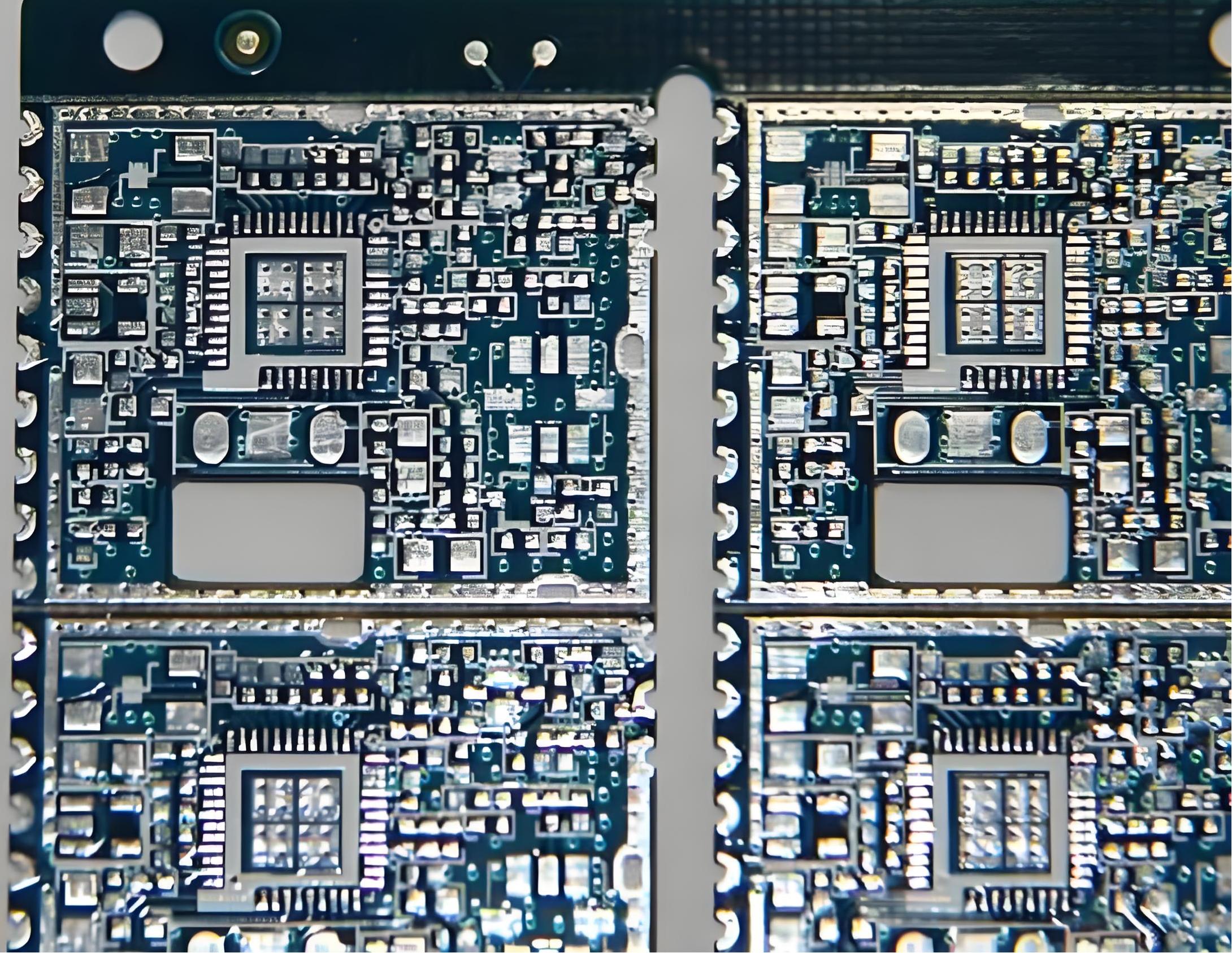
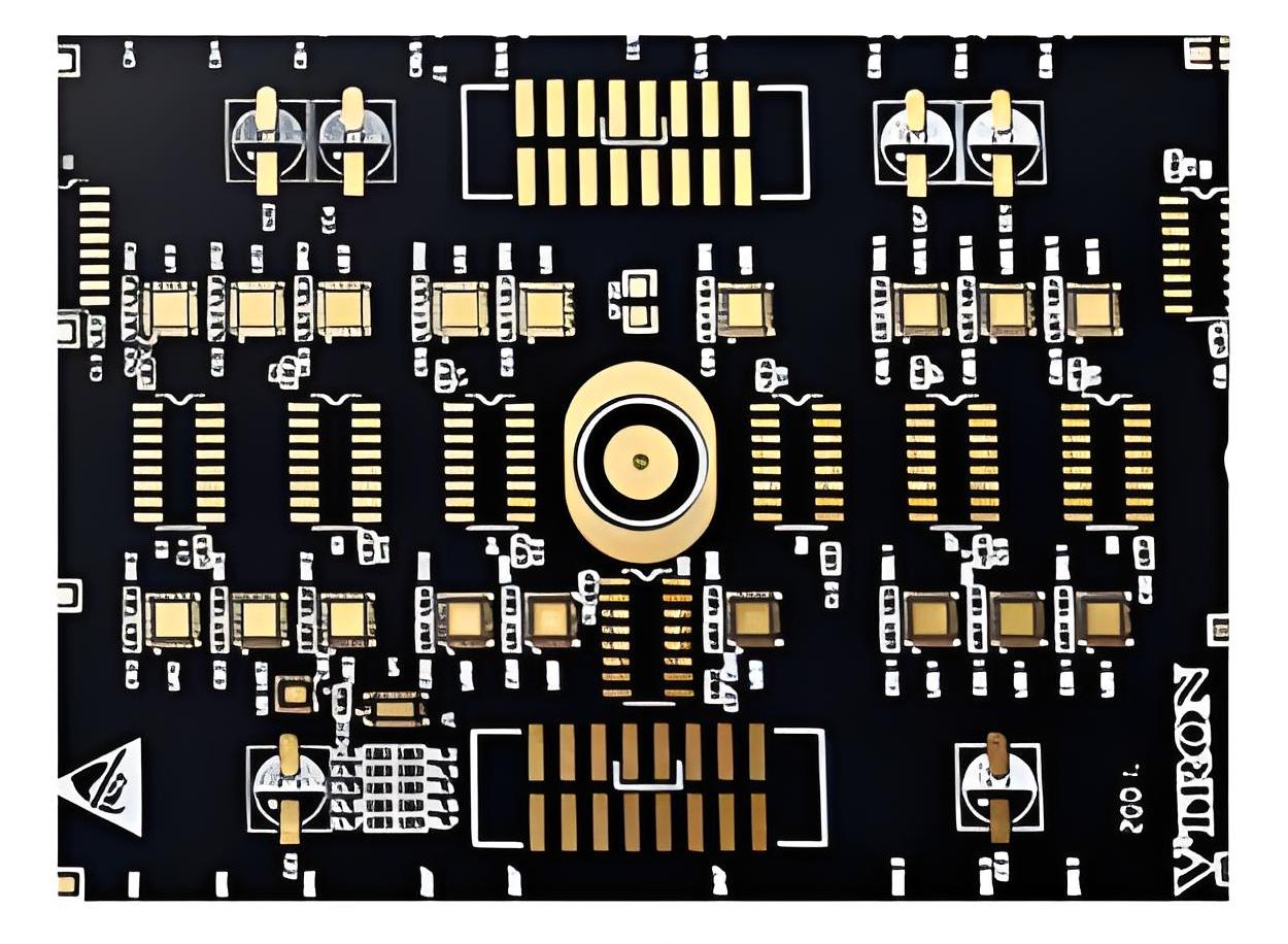
The copper layer thickness on a PCB board is usually between 1oz (35μm) and 4oz (140μm), while the copper layer thickness of a thick copper board can exceed this range, even reaching 10oz or more.
Copper layer thickness selection in different application scenarios
- Signal transmission: For signal transmission, a copper layer thickness of 1oz is usually sufficient, because signal transmission mainly focuses on signal integrity and stability.
- High current applications: For applications that need to withstand high currents, such as power supplies and industrial control equipment, 2oz or higher copper layer thicknesses are more suitable because they provide better conductivity and carrying capacity.
- Special applications: In some special applications, such as motor controllers and battery management systems for new energy vehicles, the high performance of thick copper boards can meet their stringent requirements.
What is the standard thickness of the copper layer on a PCB?
The standard thickness of the copper layer on a PCB usually ranges from 1oz to 4oz. The specific choice depends on the application scenario and requirements. For signal transmission, a thickness of 1oz is usually sufficient; for occasions that require high current, 2oz or 3oz copper thickness is more suitable.
Application scenarios of copper layers of different thicknesses
- 1oz copper thickness: suitable for general signal transmission, such as ordinary double-sided boards.
- 2oz copper thickness: suitable for occasions that require larger currents, such as power boards.
- 3oz copper thickness: suitable for high current and high power applications, such as some special industrial equipment.
The choice of copper layer thickness is mainly based on the purpose of the circuit board, the signal voltage and the current. In addition, thicker copper layers can improve the electrical performance and load-bearing capacity of the circuit board, but it will also increase the manufacturing cost.
How to calculate PCB thickness?
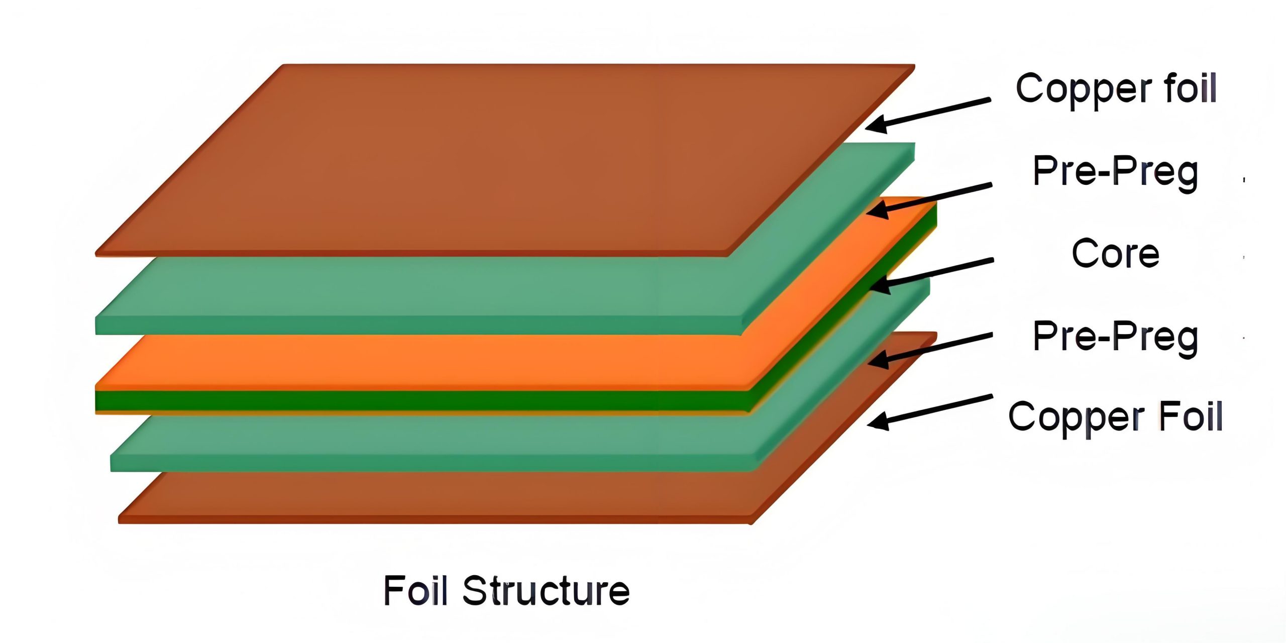
The calculation of PCB thickness mainly depends on the thickness of the copper foil and the number of layers and structure of the PCB.
The thickness of the copper foil is usually expressed in ounces (OZ), and 1OZ copper foil is approximately equal to 35 microns (um) or 1.4 mils (mil). Common PCB copper foil thicknesses are 17.5um, 35um, 70um, etc.
The thickness of the multilayer board also needs to consider the lamination loss, which is usually related to the residual copper rate of the inner copper foil. The specific formula for calculating the lamination thickness is: Lamination thickness = PP theoretical thickness – lamination loss.
What is the difference between 1oz and 2oz copper PCB?
The main difference between 1oz and 2oz copper PCBs is the thickness of the copper foil and the applicable scenarios.
1. Copper foil thickness:
- 1oz copper thickness: 1oz copper thickness means that the weight of copper foil per square foot of board area is 1 ounce (about 35.3 grams), and the corresponding copper foil thickness is about 1.4 mils (0.035mm).
- 2oz copper thickness: 2oz copper thickness means that the weight of copper foil per square foot of board area is 2 ounces (about 70.6 grams), and the corresponding copper foil thickness is about 2.8 mils (0.071mm).
2. Applicable scenarios:
- 1oz copper thickness: Suitable for most common circuit board designs and applications because it is low cost and can meet general needs.
- 2oz copper thickness: Suitable for applications that require higher current carrying capacity, such as power electronic devices and high-power LEDs.
3. Cost:
- 1oz copper thickness: It is a common choice due to its low cost.
- 2oz copper thickness: Due to the thicker copper foil, the cost is relatively high.
How thick is the copper in a flex PCB?
The copper thickness in a flexible PCB is usually 1/3 ounce (OZ), 1/2OZ, 1OZ and 2OZ, and the corresponding physical thickness is 12μm, 18μm, 35μm and 70μm respectively.
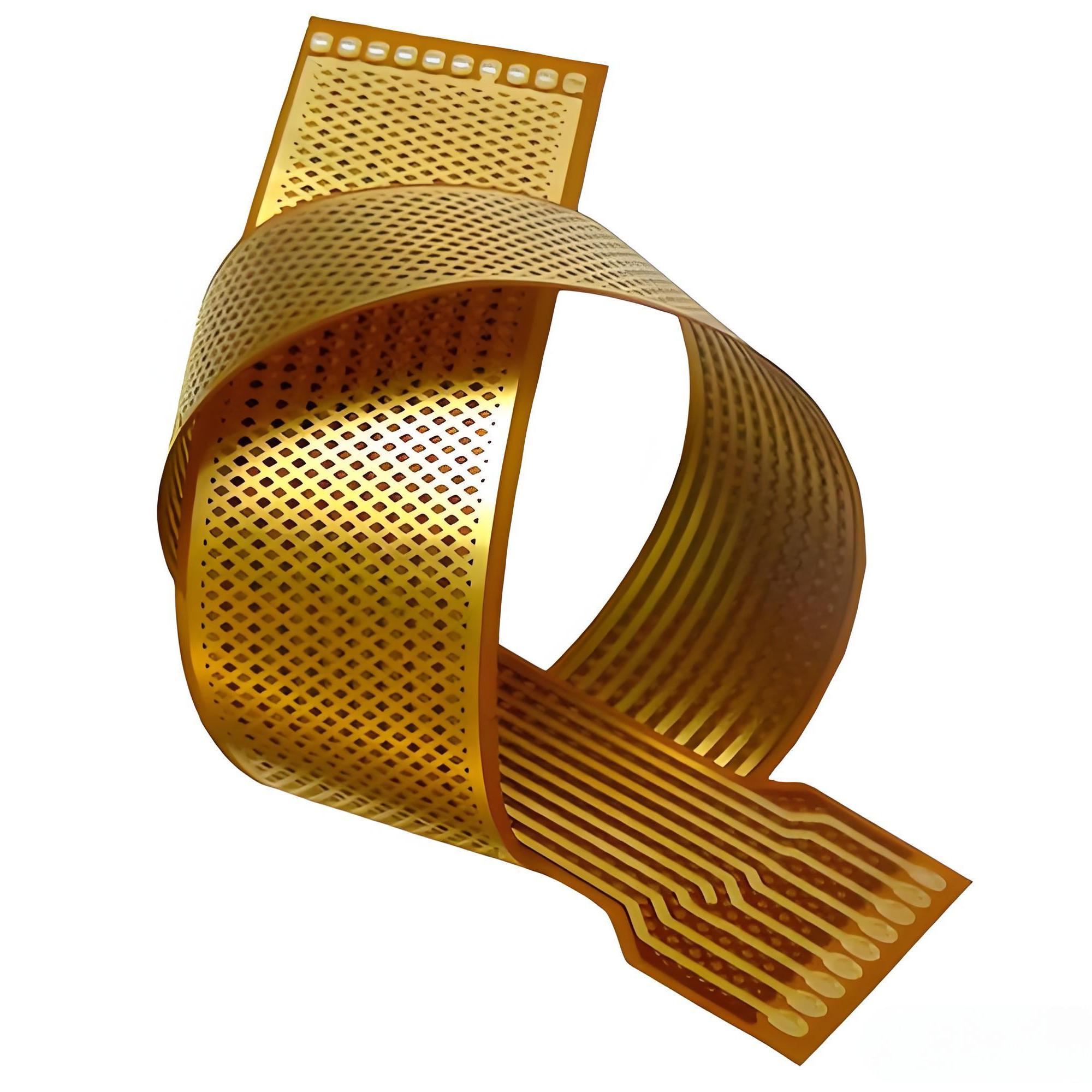
Choosing the right copper thickness is a key link in the design of flexible boards, and factors such as the application requirements, cost and technical feasibility of the circuit board need to be considered. Thicker copper foil can provide better current conduction, reduce resistance and heat generation, and improve the stability and efficiency of the circuit, but at the same time it will increase the cost and processing difficulty.
What is the thickness tolerance of copper in PCB?
The thickness tolerance standard of copper in PCB mainly depends on the type and specification of the board used.
According to the GB/T 4722 standard, the common PCB board copper thickness standard tolerances are as follows:
- 0.5mm board thickness: coarse tolerance is ±0.07mm, fine tolerance is ±0.01mm.
- 0.7mm board thickness: coarse tolerance is ±0.15mm, fine tolerance is ±0.09mm.
- 0.8mm plate thickness: rough tolerance is ±0.15mm, fine tolerance is ±0.09mm.
- 1.0mm plate thickness: rough tolerance is ±0.17mm, fine tolerance is ±0.11mm.
- 1.2mm plate thickness: rough tolerance is ±0.18mm, fine tolerance is ±0.12mm.
- 1.5mm plate thickness: rough tolerance is ±0.20mm, fine tolerance is ±0.14mm.
- 1.6mm plate thickness: rough tolerance is ±0.20mm, fine tolerance is ±0.14mm.
- 2.0mm plate thickness: rough tolerance is ±0.23mm, fine tolerance is ±0.15mm.
- 2.4mm plate thickness: rough tolerance is ±0.25mm, fine tolerance is ±0.18mm.
- 3.2mm board thickness: the rough tolerance is ±0.30mm, and the fine tolerance is ±0.20mm.
In addition, according to the IPC-6011 standard, the inner layer copper thickness tolerance is usually 10%, and the outer layer copper thickness tolerance is usually +20%. For PCBs with a thickness of less than 1mm, the board thickness tolerance is ±10% of the board thickness; for PCBs with a thickness greater than or equal to 1mm, the board thickness tolerance is ±0.10%.
How to choose PCB copper layer thickness?
There are several key factors to consider when choosing the thickness of the PCB copper layer:
- Current carrying capacity: Generally speaking, the thicker the copper, the better the electrical performance of the circuit board, and it can carry more current. For power lines or high-power applications that require large currents to pass through, using thicker copper foil can effectively reduce the temperature rise of the line and avoid performance degradation or safety issues caused by overheating.
- Signal transmission quality: Thicker copper foil can reduce wire resistance, reduce attenuation and delay during signal transmission, and thus improve signal integrity. Especially in high-frequency circuit design, precise control of copper foil thickness is the key to achieving good impedance matching, reducing signal reflection and crosstalk.
- Cost considerations: The thicker the copper, the higher the cost of the circuit board. Because thicker copper foil will increase material costs and processing difficulty, leading to an increase in overall costs.
Application scenarios Ordinary double-sided boards usually use 1oz copper thickness, while the inner layer of multi-layer boards is generally 1/2oz or 1/3oz, and the outer layer is 1oz or 1/2oz1. For circuits that require high current, 2oz or 3oz copper thickness may be used.
In short, the PCB copper thickness varies greatly. 0.5 ounce copper foil is low in cost and easy to process, suitable for simple and small products; 1 ounce is highly versatile and suitable for general electronic products; 2 ounces of copper is about 70μm thick, can carry more current, and has relatively good heat dissipation performance, but it is costly and difficult to process, and is often used in industrial equipment with extremely high power requirements. The copper thickness should be selected according to the actual situation of product function, cost, etc. to ensure that it is easy to use and economical.