If you’ve ever dealt with overheating issues or unexpected failures in automotive electronics, you know how critical PCB design is for vehicle performance and safety. Automotive circuits today handle more power than ever before, especially in electric vehicles (EVs), battery management systems (BMS), and advanced driver assistance systems (ADAS). Standard FR4 PCBs with typical 1oz or 2oz copper layers often struggle to meet these demands.
This is where 4oz copper PCBs step in. But what exactly is a 4oz copper PCB, and why does it matter so much in automotive electronics? In this blog, we’ll explore the fundamentals, compare it to standard options, and show you how it can improve your vehicle designs across the board.
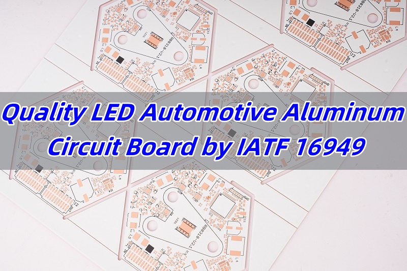
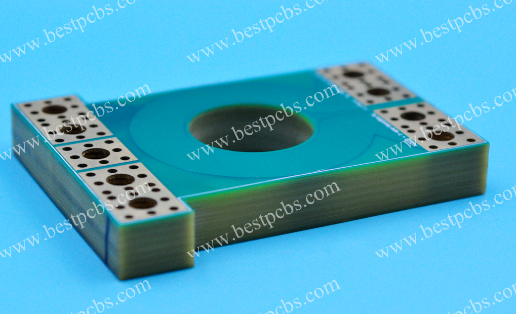
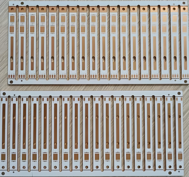
4oz Copper PCB for Automotives
What Is 4oz Copper PCB?
In PCB manufacturing, “oz” refers to the weight of copper per square foot of board surface. One ounce (oz) corresponds roughly to a copper thickness of 35 micrometers (µm). Therefore, a 4oz copper PCB has approximately 140µm of copper thickness—about four times thicker than a standard 1oz copper PCB.
This increase in copper thickness means the PCB can carry higher currents without overheating. The thicker copper layer also spreads heat more effectively, reducing hotspots and improving the board’s durability under thermal stress. These features are especially important in automotive environments, where electronics are exposed to high temperatures and heavy current loads.
1oz~4oz Copper PCB Thickness
Let’s break down the copper PCB thickness range for better understanding:
| Copper Weight | Approx. Thickness (µm) | Max Current (10mm trace) |
| 1oz | 35µm | ~10A |
| 2oz | 70µm | ~20A |
| 3oz | 105µm | ~30A |
| 4oz | 140µm | 40A+ |
As you move from 1oz to 4oz, the copper layer becomes significantly thicker and handle more current and allow for more current flow. While 1oz and 2oz are suitable for signal layers or low-power modules, 4oz copper PCBs are designed for high-power circuits. That’s why 4oz copper pcb is a preferred choice in automotive systems where reliability and thermal control are paramount.
Benefits of 4oz Copper PCB in Automotives
- A thicker copper layer means you can run higher currents without overheating or damaging the traces.
- 4oz PCBs handle heat much better. This is especially useful in high-temperature zones like under the hood.
- With more copper, the PCB becomes more robust and less likely to break or warp during vibration or shock.
- Automotive systems need to last years. Thicker copper extends the life of the circuit board, even in aggressive environments.
- Instead of using multiple layers to handle current, a 4oz PCB can do it in fewer layers, saving board space and reducing weight.
Comparison with Standard PCBs for Automotives
While standard PCBs using 1oz or 2oz copper can handle simple functions—like dashboard indicators or infotainment controls—they fall short in high-current, high-temperature applications. This is where a 4oz copper PCB makes a real difference.
Automotive environments are harsh. The electronics must endure constant vibration, wide temperature shifts, and demanding power loads. A 4oz copper PCB provides thicker conductive paths that can safely handle larger currents without overheating. This is crucial in systems like:
- Electric vehicle (EV) battery packs
- Motor controllers and inverters
- LED headlamp circuits
- Power distribution units (PDUs)
- ABS and electric steering systems
When to Use 4oz Copper PCB?
Not every automotive application needs 4oz copper. It’s best used when:
- The circuit needs to carry large currents continuously
- The design requires strong heat resistance
- There’s limited space for large traces or cooling systems
- The board operates in harsh environments like engine bays or near power inverters
- The product is mission-critical, such as for braking systems or EV battery controls
You don’t want to overengineer a simple circuit. But if you’re designing for performance, durability, or safety, a 4oz copper PCB can be the right investment.
Capabilities Needed for High-Quality 4oz Automotive PCBs
Building a 4oz PCB isn’t just about adding more copper. It requires advanced production techniques. Here’s what to look for in a PCB manufacturer:
- Precision Etching Technology: Thick copper makes fine line control more difficult. Only experienced manufacturers can maintain accurate trace geometry.
- Heavy Copper Lamination Skills: 4oz copper needs proper lamination to avoid delamination or blistering during thermal cycles.
- Reliable Drill and Plating Process: Via reliability is critical when dealing with heavy copper. The plating must be uniform and strong.
- Controlled Impedance Design: Even thick copper PCBs need proper signal integrity for communication modules.
- Stringent Testing: Including thermal shock, solderability, and ionic contamination tests to ensure reliability in real-world automotive conditions.
Without these capabilities, the risk of product failure or performance drop increases. Choose wisely when it comes to manufacturing partners.
Key Indicators of 4oz PCB Manufacturing Quality
If you’re sourcing 4oz copper PCBs, here are some signs of a quality supplier:
- Consistent Copper Thickness: Actual copper weight matches the design specs throughout the board.
- No Over-Etching or Undercut: Clean trace edges even at high copper weights.
- Low Warpage: Even with 4oz copper, the board stays flat and stable.
- Smooth Surface Finish: Whether ENIG, OSP, or HASL, surface finish quality reflects the overall manufacturing process.
- Comprehensive Testing Reports: Good manufacturers share test data, like cross-section analysis or microvia inspection.
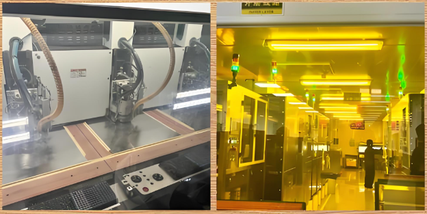
Benefits of Partnering with EBest Circuit (Best Technology)
At EBest Circuit (Best Technology), we specialize in high copper PCBs for automotive and power applications. Here’s why global clients trust us:
- We have more than 19 years experiences in this industry, and we have matured techniques to manufacture 4oz or heavier thickness copper PCB.
- Our sales are originated from engineers., they can provide the professional suggestions that based on engineers aspects, so you do not need to pay much time to wait an answer from engineer department.
- Our team helps you optimize trace width, via sizes, and stack-up to make your design work with 4oz copper. we know how to do and how to optimize to achieve the best performance.
- We are IATF16949 certified, ensuring our production lines meet strict automotive quality standards.
- Every board is tracked, from raw material to shipment, giving you complete process transparency.
- From AOI to flying probe, we inspect every stage to ensure tight tolerances and excellent repeatability.
- Whether you’re a startup or OEM, our support team makes sure your needs are met, from quotation to delivery.
FAQs
1. What current can a 4oz copper PCB carry?
Depending on trace width and cooling conditions, 4oz copper can safely handle currents exceeding 50 amps in many automotive applications.
2. Can 4oz PCBs be used in multilayer automotive boards?
Yes, thick copper layers are compatible with multilayer boards, but stack-up design must carefully consider heat dissipation and mechanical stresses.
3: Can I use a 4oz copper PCB in consumer electronics?
You can, but it’s usually not necessary unless the product requires high current flow or superior thermal performance.
4. Are 4oz PCBs compatible with HDI automotive designs?
They can be, but HDI PCB designs require precise control of trace dimensions and vias; working with an experienced supplier is key.
5. Does EBest Circuit (Best Technology) offer UL or automotive-grade testing?
Yes, we provide comprehensive testing services including UL certification support and automotive qualification testing per your needs.
If you have any questions about 4oz copper PCB or automotive PCBs, you are welcome to contact us at sales@bestpcbs.com. Our guys are 24/7 online to serve you!