High speed board design is central to advanced electronics today. In this blog, we mainly talk about how to design and manufacture a top-quality high speed board PCB, focusing on both fundamentals and practical guidelines.
Do you have issues with these aspects?
- High complexity of design and long design cycle?
- The problem of signal completeness?
- The issues of manufacturing and production? For example, when you need quick prototypes to be developed or small batch manufacturing, but the traditional manufacturer is struggling to meet these demands.
- High cost and time investment?
Below are the complete solutions for addressing the above issues.
- Enhance the design process and tools: EBest Circuit (Best Technology) presents high speed board design guidelines and expert support, which helps customers to tackle potential problems in the design phrase.
- Boost manufacturing capability: EBest Circuit (Best Technology) offers automatic production lines and cutting-edge manufacturing processes, such as SMT, AOI, and MES systems, to increase manufacturing efficiency and product quality.
- Elevate the design of signal completeness: EBest Circuit (Best Technology) provides a customizable design service, and we give quick solutions for the specific applications, such as high frequency, high speed, and high reliability applications.
- Strengthen customer support and collaboration: EBest Circuit (Best Technology) supplies the complete service from design and manufacturing, including engineering design, process design, testing, and others.
EBest Circuit (Best Technology) provides technical guidance and order process support, aiming to help customers better understand and apply high-speed PCB design and manufacturing techniques. We have our original PCB and PCB factory, and we can directly coordinate the manufacturing schedule. If you require any high-quality, high-speed board PCB, please contact us directly at sales@bestpcbs.com.
What is a high speed board?
High speed boards are defined by how signals behave when rise times are very short, not only by their clock frequency.
- Signal rise time: A 100 MHz signal with a 200 ps rise time behaves like a GHz waveform, requiring controlled impedance.
- Applications: Networking switches, 5G base stations, aerospace avionics, high-speed servers, and automotive radar.
- Design focus: Transmission line effects, reflections, and crosstalk dominate performance at these speeds.
- Engineering challenge: Even a few millimeters of extra trace can distort signals when rise times are sub-nanosecond.
High speed boards are about edge rates and timing integrity, forming the foundation for reliable modern PCB design.
What is the difference between high speed board and high-frequency PCB?
These terms are often confused, yet they describe different design needs.
- High-frequency PCB: Focused on operating frequency, usually above 1 GHz, common in RF and microwave circuits.
- High speed board: Focused on fast edge transitions, even at lower base frequencies.
- Design overlap: Both need low-loss materials, impedance control, and clean layouts, but analysis differs.
- Customer pain point: Wrong board choice often leads to wasted cost or unreliable performance.
| Aspect | High-Frequency PCB | High Speed Board |
|---|---|---|
| Main concern | Operating frequency (GHz) | Signal rise time (ps/ns) |
| Applications | Antennas, radar, RF | Digital circuits, networking |
| Key factor | Dielectric constant stability | Timing, impedance, crosstalk |
Choosing the right type depends on whether your challenge is high carrier frequency or fast switching signals.
What is the frequency of a High speed board pcb?
Frequency alone does not define speed, but it still matters in many designs.
- Range: High speed boards typically handle signals from hundreds of MHz up to several GHz.
- Edge factor: A 500 MHz signal with steep edges may behave like a 2 GHz design in terms of layout needs.
- Customer impact: Underestimating this relationship causes noise, jitter, and unreliable data transfer.
- Industry note: Many Ethernet standards (10G, 25G, 100G) rely on high speed boards with effective frequency in multi-GHz ranges.
Designers must evaluate both signal frequency and rise time to decide when high speed techniques are required.
What is the best PCB material for high speed board?
PCB materials directly influence losses, delay, and overall stability in high speed designs.
- FR4: Cost-effective but suffers high loss above 3–5 GHz.
- Low-loss laminates: Rogers (RO4000, RO3000 series), Panasonic Megtron, Taconic are popular choices.
- Dielectric constant (Dk): Materials with stable Dk minimize delay and skew.
- Dissipation factor (Df): Lower Df reduces signal loss, vital for multi-GHz signals.
- Customer concern: Overspending on premium materials when FR4 is sufficient for mid-speed designs.
| Material | Dielectric Constant (Dk) | Dissipation Factor (Df) | Typical Use |
|---|---|---|---|
| FR4 | ~4.2 | 0.020–0.025 | General, <5 GHz |
| Rogers RO4350B | 3.48 | 0.0037 | 5G, RF, high-speed |
| Megtron 6 | 3.4 | 0.002–0.003 | High-speed networking |
The best choice balances performance and budget, with EBest Circuit (Best Technology) offering material guidance tailored to customer needs.
How to do High-speed circuit design?
High-speed circuit design requires more than simple routing. At these speeds, signal integrity, impedance control, and layout accuracy are essential. EBest Circuit (Best Technology) helps engineers overcome common pitfalls.
Key steps in high-speed circuit design:
- Controlled impedance traces: Ensure PCB traces match the required impedance to minimize reflections.
- Minimize stubs: Long stubs create reflections; avoid or shorten them as much as possible.
- Ground planes: Use continuous ground planes under signal layers to reduce EMI and improve return paths.
- Via optimization: Reduce the number of vias on critical signal paths to maintain signal quality.
- Layer stack-up planning: Proper stack-up ensures signal integrity and reduces crosstalk between layers.
- Decoupling capacitors: Strategically place capacitors near ICs to stabilize voltage rails.
A successful high-speed circuit design balances performance, manufacturability, and cost. EBest Circuit (Best Technology) provides layout review and engineering consultation to help achieve optimal designs.
Why use a high speed board to board connector in PCB design?
Board-to-board connectors play a critical role in high-speed systems. They enable modular designs and reliable signal transfer between multiple boards.
Benefits of using high-speed board-to-board connectors:
- Signal integrity: Designed to maintain controlled impedance for fast signals.
- High-density routing: Allow compact designs without long traces between boards.
- Mechanical stability: Secure connections reduce vibration-induced signal degradation.
- Ease of assembly: Simplifies modular PCB designs and reduces assembly errors.
- Customer pain point: Many designers face unreliable interconnects; using proper connectors prevents signal loss.
High-speed board-to-board connectors ensure reliable communication between boards, reducing debugging and improving system stability.
How to reduce noise in high speed board?
Noise and EMI are major challenges in high-speed PCBs. Controlling them is crucial for reliable signal transmission.
Effective noise reduction techniques:
- Grounding strategy: Continuous ground planes and proper via stitching reduce noise.
- Trace spacing: Maintain spacing to reduce crosstalk between adjacent traces.
- Differential pairs: Use differential routing for high-speed signals to cancel noise.
- Shielding: Shield critical traces or areas to prevent EMI interference.
- Decoupling capacitors: Filter high-frequency noise near ICs.
Proper planning and noise mitigation strategies ensure high-speed boards perform reliably. EBest Circuit (Best Technology) can advise on PCB layout to minimize EMI and crosstalk.
How to test High speed board PCB?
Testing is critical to verify high-speed PCB performance. Early detection of problems saves cost and ensures reliability.
Key testing methods:
- Time Domain Reflectometry (TDR): Measures impedance discontinuities in traces.
- Vector Network Analyzer (VNA): Tests frequency response and signal loss at GHz ranges.
- Signal eye diagrams: Verify timing integrity and signal quality.
- Automated Optical Inspection (AOI): Checks for solder defects and shorts.
- Functional testing: Simulates real-world signals to ensure full system reliability.
Comprehensive testing ensures high-speed boards meet performance specifications. EBest Circuit (Best Technology) uses advanced testing to deliver reliable products to customers.
How to improve High-speed signals in PCB?
Maintaining signal quality is essential for high-speed boards. Even small layout or material errors can degrade signals.
Techniques to improve high-speed signals:
- Impedance matching: Match trace impedance with driver and receiver for minimal reflection.
- Minimize trace length: Shorter traces reduce delay and signal loss.
- Differential routing: Use tightly coupled differential pairs for better noise immunity.
- Proper via design: Limit vias in high-speed paths; use back-drilling if needed.
- Layer separation: Separate high-speed signals from noisy power or analog layers.
| Method | Effect |
|---|---|
| Controlled impedance | Reduces reflections |
| Differential pairs | Cancels noise |
| Proper via usage | Maintains signal integrity |
| Short trace length | Minimizes delay and attenuation |
| Ground planes | Reduces EMI and provides return path |
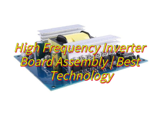
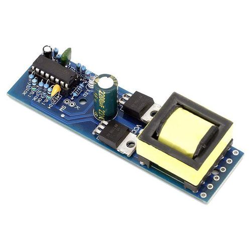
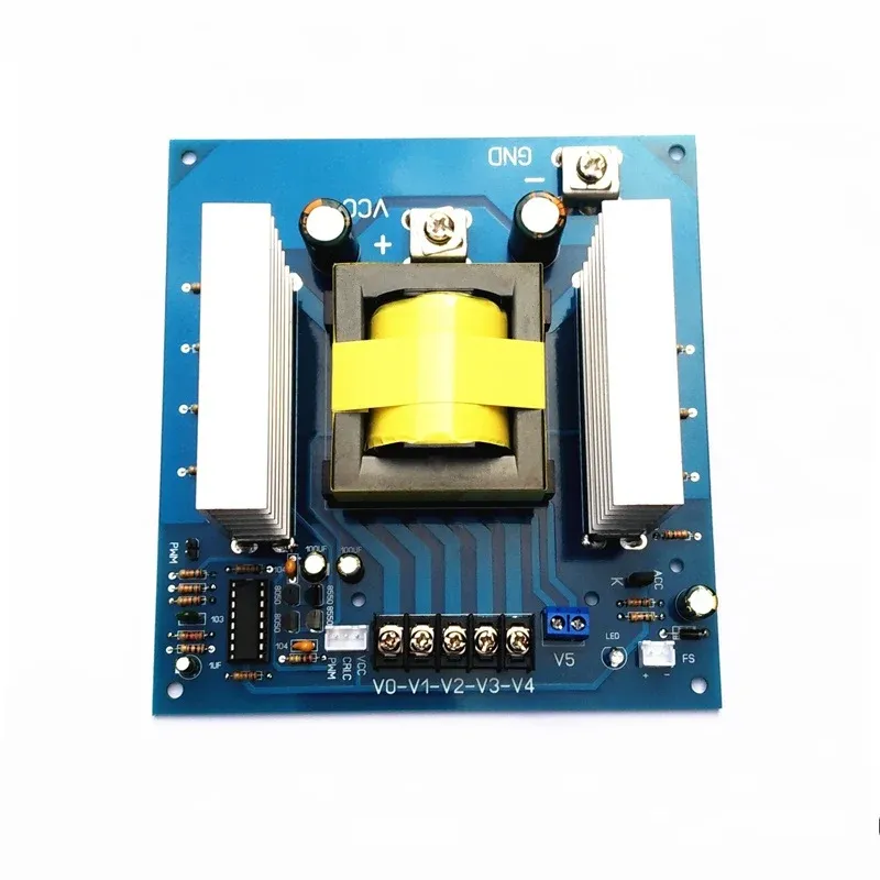
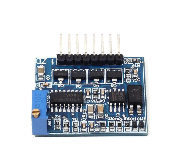
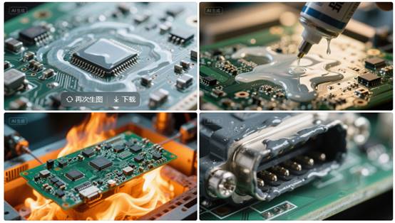
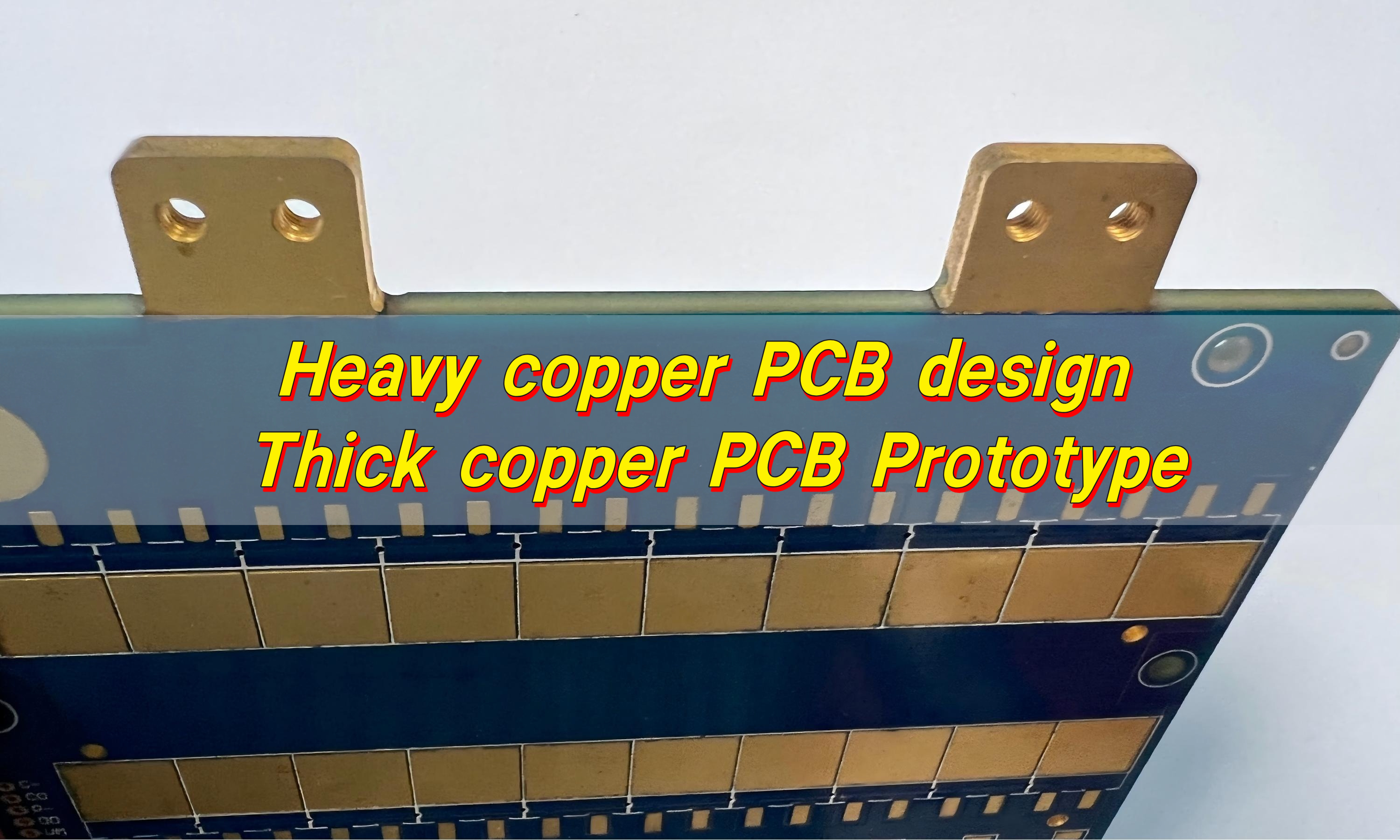
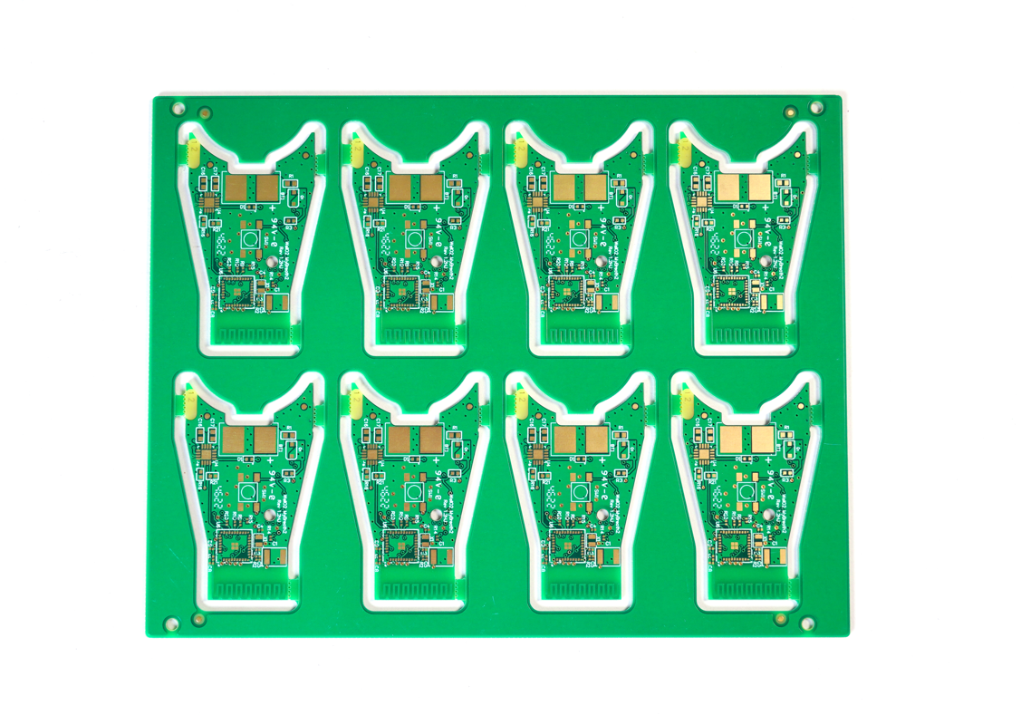
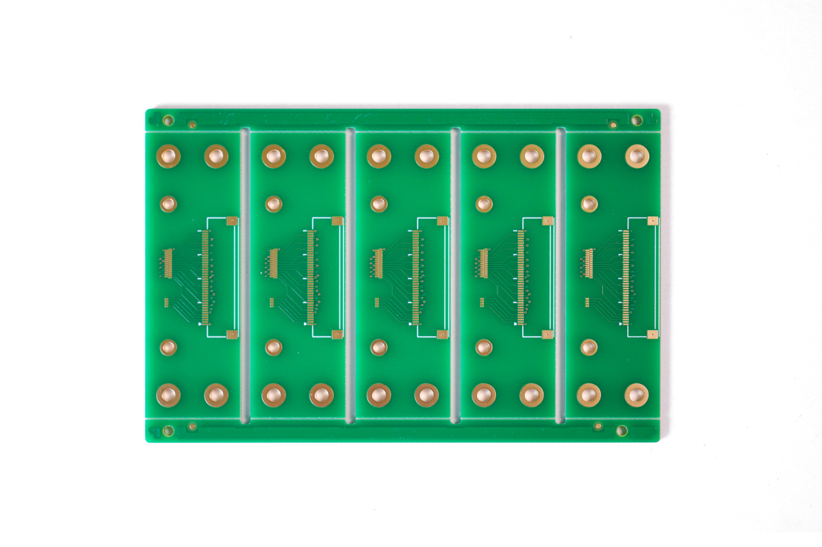
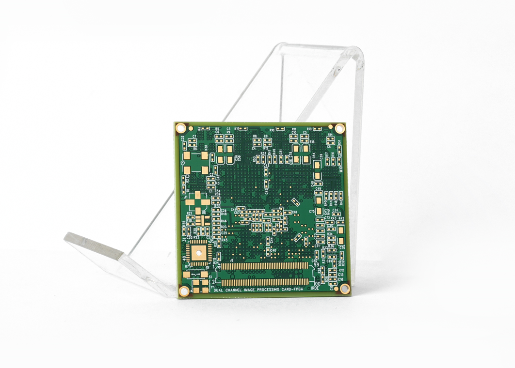
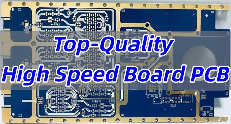
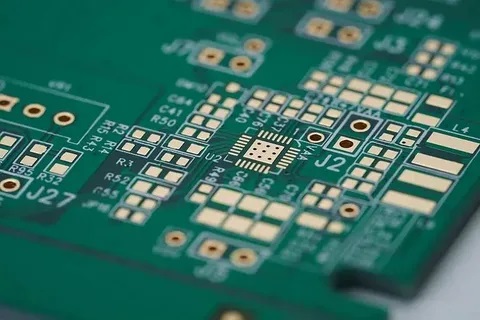
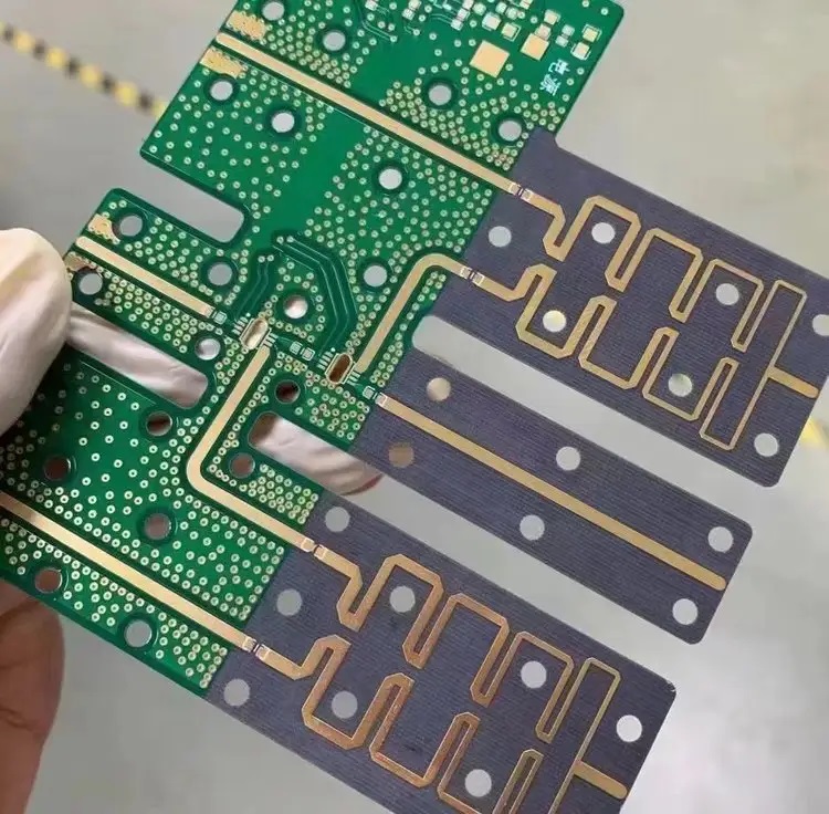
Case about High Speed Board in EBest Circuit (Best Technology)
High-speed boards are applied in a huge range of industries, such as 5G networks, RF and microwave systems, telecommunications, and others. Here are some of our high-speed PCB board pictures for your review.
To sum up, optimizing high-speed signals requires careful layout, material selection, and testing. EBest Circuit (Best Technology) supports customers with design guidelines and design review to achieve clean, reliable signals. We are happy to give our full engagement to you for your prototypes, mass production, or assembly needs. Now our PCBs have been sold to America, Germany, and other countries. A warm welcome to contact us at sales@bestpcbs.com for help.