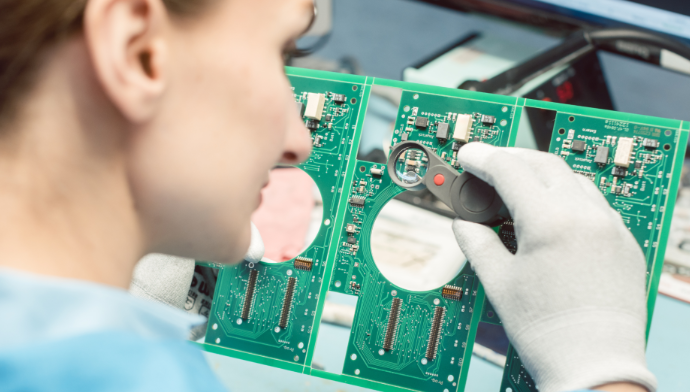
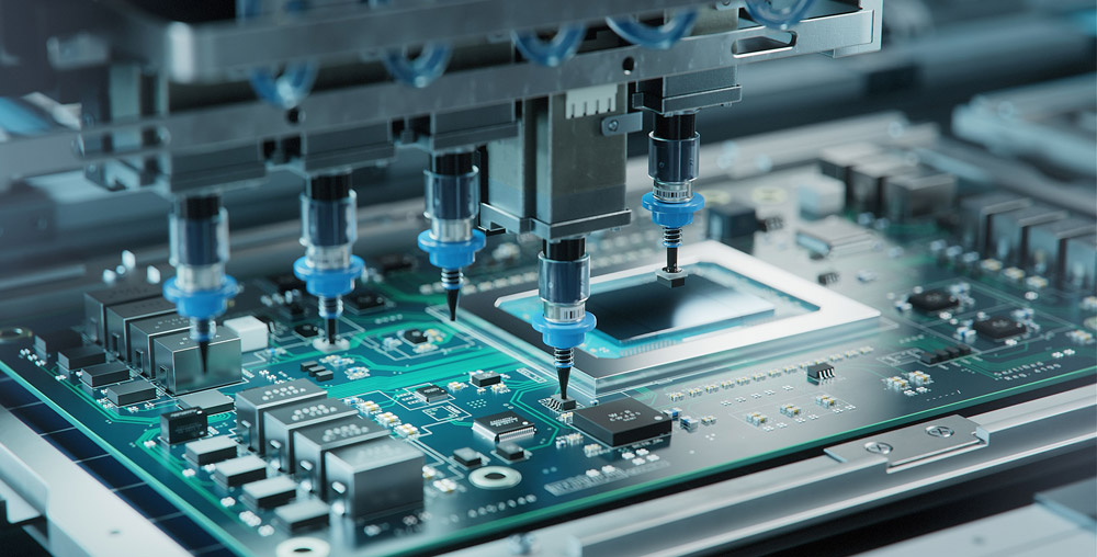
Soldering remains one of the most fundamental operations in electronics manufacturing, and its reliability depends on far more than just heat and solder alloy. Flux is a quiet but powerful material that determines how well a solder joint forms, how stable the connection remains over time, and how durable a finished PCB assembly will be in the field.
For new engineers, technicians, and even seasoned designers, misunderstandings about flux are common—especially around topics such as electrical conductivity, residue behavior, and flux selection for different soldering environments. This guide provides a detailed but easy-to-read explanation of what flux is, what it does, and whether it conducts electricity. It also highlights practical considerations for real PCB assembly workflows.
What Is Flux in Soldering?
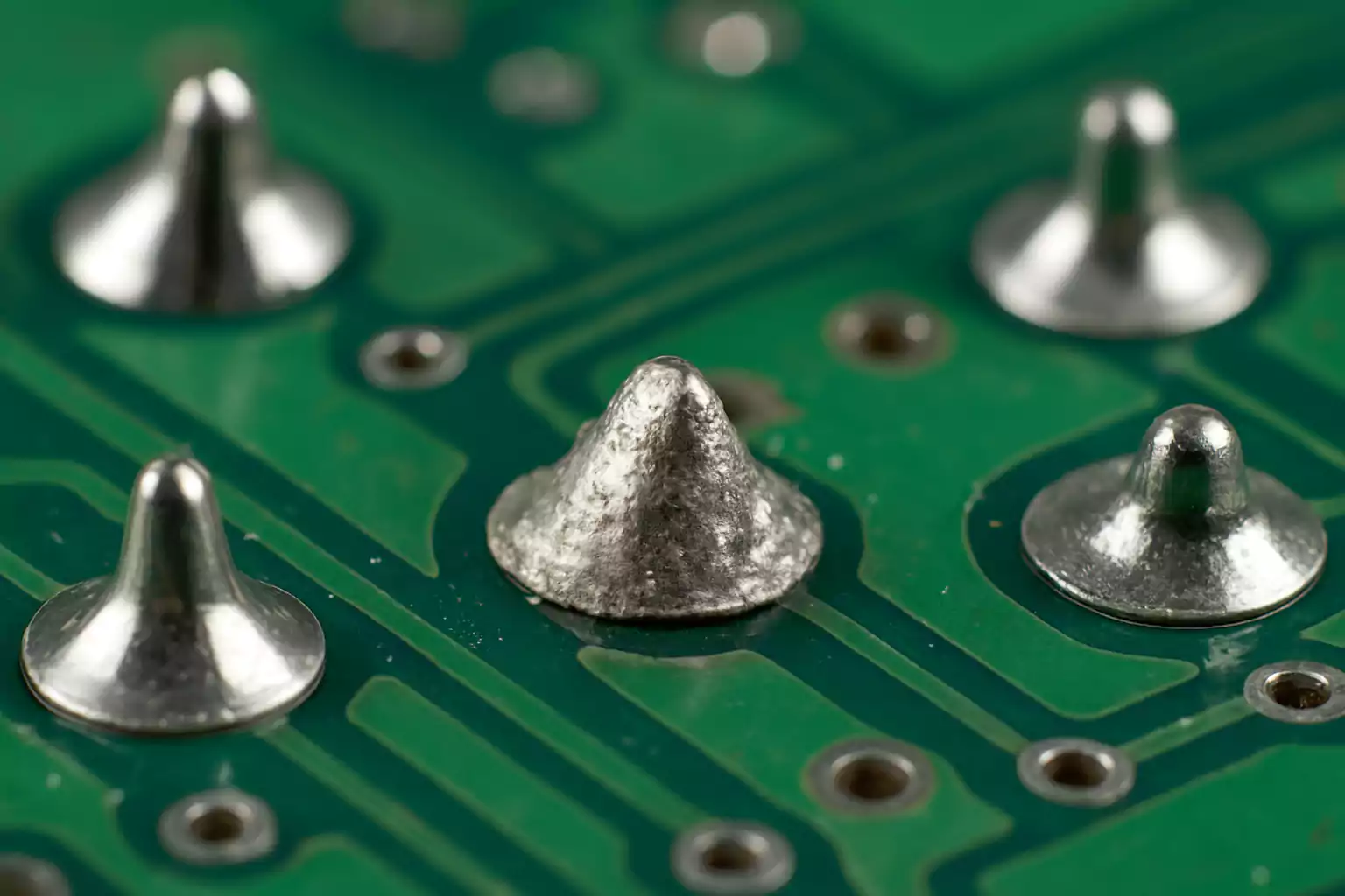
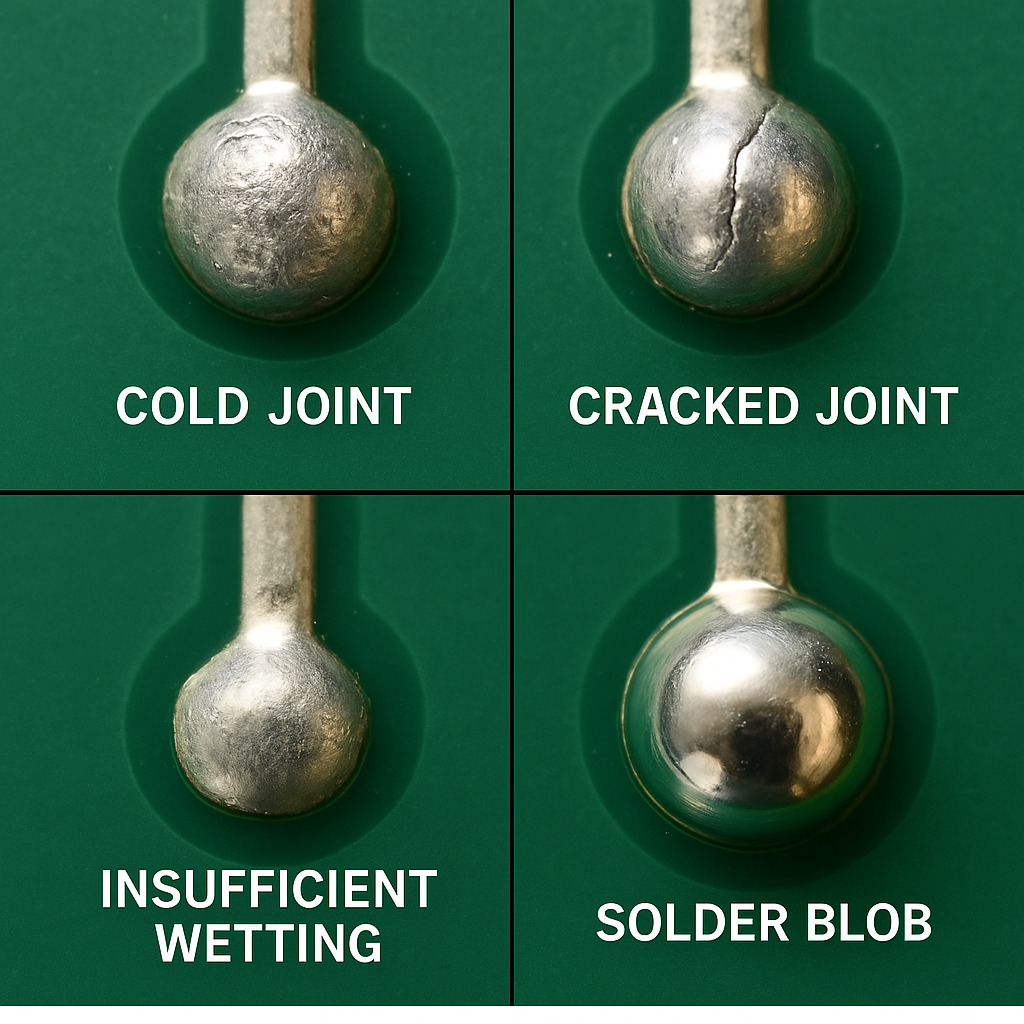
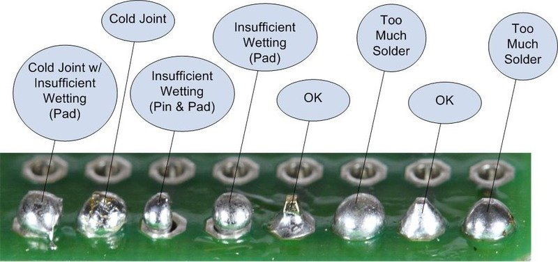
Flux is a chemical agent applied during soldering to prepare metal surfaces and support the formation of reliable solder joints. When copper pads or component leads are exposed to air, oxidation naturally occurs. Even a microscopic layer of oxidation can obstruct solder wetting, causing poor joints, voids, and insufficient fillets.
Flux removes these oxides, shields the surface from further oxidation during heating, and helps molten solder spread smoothly across metal surfaces. It improves consistency, lowers defect rates, and stabilizes the soldering process across different alloys and temperatures.
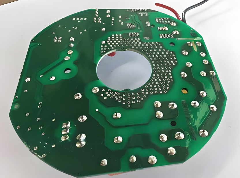
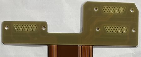
In PCB assembly—whether reflow, wave soldering, or selective soldering—flux is as essential as the solder itself. Without it, joints would frequently fail, especially on components with small contact areas or on boards that require high-density interconnects.
Is Flux the Same as Solder?
Flux and solder are very different materials, even though both are packaged together in solder wire or solder paste.
- Solder is a metal alloy that melts and forms the electrical and mechanical connection.
- Flux is a chemical compound that prepares the surface and improves the solder’s ability to bond.
Flux does not create a joint by itself. It does not replace the solder alloy. Instead, it ensures the solder achieves a strong, durable bond with copper pads and component leads.
During soldering, flux activates first. As heating continues, solder alloy becomes molten and flows into the prepared surface, producing a joint that is structurally sound and electrically stable.
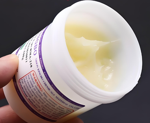
What Is Flux Made Of?
Flux formulations differ depending on application, activity level, and cleaning requirements, but most contain three major components:
1. Base Material
This forms the bulk of the flux. Common bases include:
- Rosin (natural resin from pine trees)
- Synthetic resin
- Organic acids
- Water-soluble organic compounds
2. Activators
These compounds remove oxides and enable solder wetting. Examples include:
Halides and halogen-free activators
- Organic acids
- Amines
Activators determine how aggressive the flux is and directly influence cleaning requirements.
3. Solvents
Liquids that adjust viscosity and allow the flux to spread evenly. Depending on the type, the solvent may be:
- Alcohol-based
- Water-based
- Mixed solvent systems
Additional additives control stability, residue appearance, heat resistance, and spread behavior.
In solder paste, flux is blended with metal powder (tin-based alloy particles). In liquid or pen flux, the chemical composition varies more widely depending on the intended soldering method.
Types of Flux Used in Electronics Soldering
Flux comes in multiple varieties because different electronic assemblies require different performance and cleaning levels.
1. Rosin Flux (R, RMA, RA)
A classic formulation used for decades.
- R (Rosin): Mild, minimal activity
- RMA (Rosin Mildly Activated): Balanced activity and reliability
- RA (Rosin Activated): Strong oxide removal; requires cleaning
Rosin residues are typically hard and non-corrosive but still benefit from cleaning in sensitive electronics.
2. No-Clean Flux
Designed to leave minimal residue that remains safe on the board.
- Very low activity
- Ideal for high-volume consumer products
- Popular in SMT reflow
However, no-clean flux is not “no-clean” for everything. High-reliability sectors such as medical, aerospace, and automotive often still require cleaning.
3. Water-Soluble Flux
It is a strong, highly active flux. It can:
- Removes heavy oxidation
- Excellent wetting performance
- Residue is conductive and must be cleaned with water
This flux is common for BGA, QFN, and fine-pitch applications due to its high activity.
4. Flux Paste, Gel, Liquid, and Pen Types
Each soldering method favors a different form:
- Flux paste: Hand soldering, rework
- Liquid flux: Wave soldering and selective solder
- Gel flux: BGA sphere attachment and reballing
- Flux pens: Small-area touch-ups
Choosing the right format ensures controlled application and stable process quality.

What Are the Functions of Flux in Soldering?
The main active component in the soldering agent is rosin. Rosin will be decomposed by tin at around 260 degrees Celsius. Therefore, the temperature of the soldering bath should not be too high. In soldering, it is an indispensable auxiliary material and plays an extremely important role.
- Removes surface oxides from copper pads and component leads.
- Prevents re-oxidation during heating.
- Improves solder wetting, allowing the alloy to spread uniformly.
- Reduces surface tension, enabling smoother flow.
- Promotes mechanical strength, making joints more reliable.
This combination ensures repeatable and stable solder connections for both prototype and mass production builds.
Is Flux Conductive?
Fresh flux and properly cleaned flux residue are not conductive. Most fluxes are designed to be electrically insulating, even when left on the PCB after reflow or hand soldering.
This is why no-clean flux can remain on many consumer-grade boards without impacting function.
Why Some Flux Residues Become Slightly Conductive?
Although flux itself is non-conductive, residue can become slightly conductive under certain conditions, especially with:
- Water-soluble (OA) flux
- Highly activated flux
- Flux that absorbs humidity over time
- Ionic contamination left behind after incomplete cleaning
This moisture-dependent conductivity may cause leakage paths, corrosion, or unpredictable behavior in sensitive analog, RF, or high-impedance circuits. That is why aerospace, medical, and automotive assemblies often require a thorough post-cleaning process.
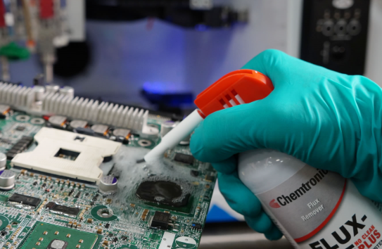
Best Cleaning Methods for Flux Residue
Different assemblies require different cleaning approaches, but the goal is always the same: remove unwanted residue without damaging components or altering board performance. Selecting the right method depends on the flux type, the board’s cleanliness requirements, and the equipment available in your production line.
- Isopropyl Alcohol (IPA) Wipe or Brush Cleaning
IPA remains one of the simplest and most effective ways to remove rosin-based flux. A soft brush or lint-free wipe helps dissolve residue quickly, making it ideal for rework, repair, or small-batch builds.
- Precision Flux Remover Sprays
Engineers often choose specialized flux remover sprays for dense assemblies or harder residues. These solutions penetrate tight spaces under components and evaporate cleanly. They are especially helpful when dealing with no-clean flux that has carbonized during reflow.
- DI Water Cleaning for Water-Soluble Flux
Water-soluble (OA) flux requires complete removal because it contains ionic materials. DI water cleaning, either by hand or in an automated system, rinses away these residues effectively.
- Ultrasonic Cleaning
For assemblies with fine-pitch packages, BGA components, or complex geometries, ultrasonic cleaning can reach areas traditional brushing cannot. High-frequency waves dislodge residue in hidden spaces. Not all components tolerate ultrasonic energy, so a controlled process is essential.
Common Mistakes When Using Flux
Many soldering issues trace back to improper use of flux. Common mistakes include:
- Applying excessive flux, which can trap residue under components
- Mixing different flux types in the same process
- Using expired flux that has lost its activity
- Selecting a flux that does not match the solder alloy or temperature profile
- Not cleaning when required by the flux classification
A disciplined approach helps avoid rework and enhances long-term reliability.
How to Choose the Right Flux for Your Soldering Process?
Select flux based on your assembly method, product reliability, and cleaning capability:
1. Consider the soldering process
- SMT reflow often uses no-clean or RMA flux.
- Wave soldering may need higher-activity flux.
- Hand soldering typically requires easily reactivated flux pens.
2. Match reliability requirements
- High-reliability industries prefer water-soluble flux with full cleaning.
- Consumer electronics often adopt no-clean materials.
3. Check board materials and surface finishes
For example, ENIG, OSP, and HASL may react differently to flux activity.
4. Account for reflow temperature
Some fluxes degrade if overheated, reducing wetting efficiency.
FAQs
1. Can you solder without flux?
It is possible but not recommended. Flux ensures strong wetting and consistent joints.
2. Is no-clean flux truly “no clean”?
In most consumer applications, yes. For high-reliability products, cleaning may still be required.
3. Does flux expire?
Yes. Its activity decreases over time, which affects soldering quality.
4. Is flux harmful to PCBs?
Not when used correctly. Incorrect cleaning or high-activity residues may cause long-term issues.
5. Why does flux smoke during soldering?
Flux evaporates and burns off as it activates. This is normal.
6. Which flux is best for sensitive electronics?
Low-residue no-clean flux or water-soluble flux with full cleaning.