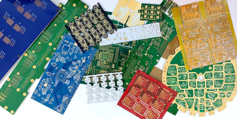
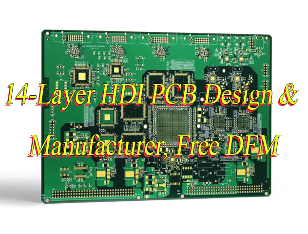
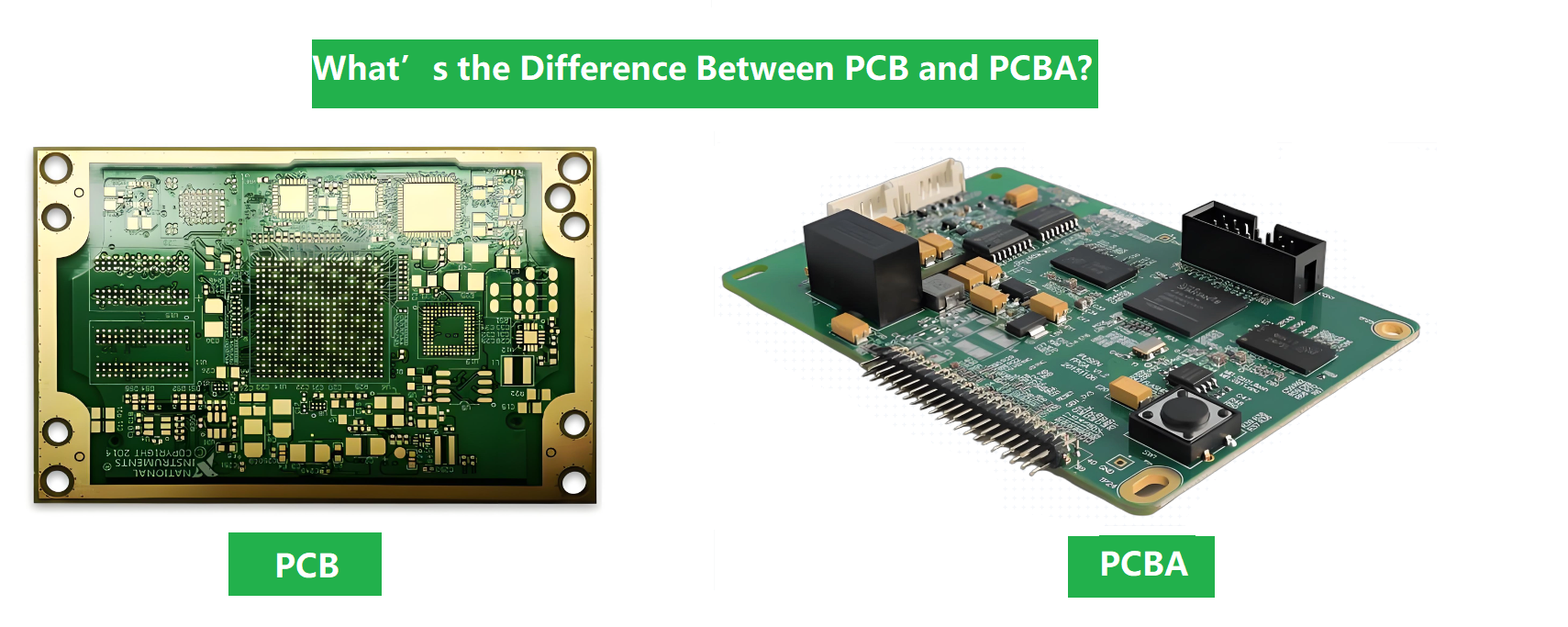
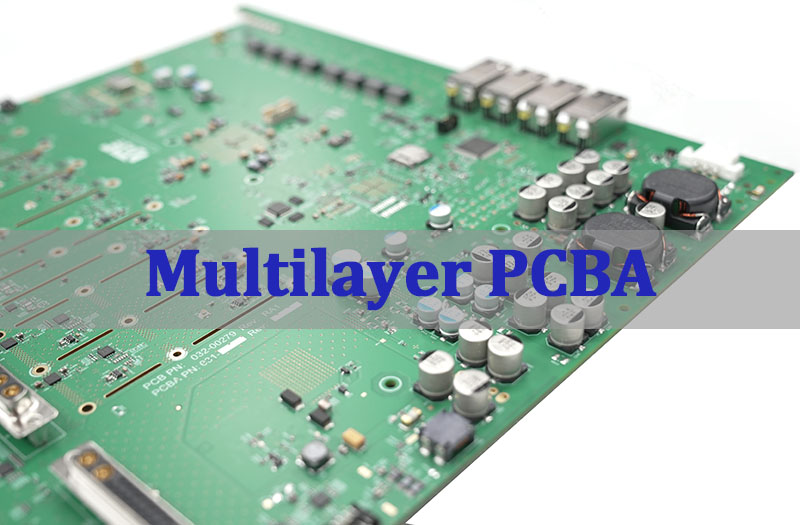
Multilayer PCBA is the practical way to integrate dense routing, controlled impedance, and stable interconnects into compact medical electronics where signal integrity and reliability must hold up in real use. This article explains the engineering controls, standards, materials, manufacturing flow, and application choices that make Multilayer PCBA Manufacturing in China for Medical Electronics both scalable and dependable.
Which Process Risks Most Often Affect PCBA Assembly Multilayer?
- Stack-up assumptions drift from the real board build, causing impedance and EMI surprises.
- Via quality and plating variability leads to intermittent opens under thermal cycling.
- Warp and twist create BGA/QFN solder defects and unstable test yields.
- Material and finish mismatch triggers delamination risk or poor solderability in rework.
- Inspection gaps and weak test coverage allow latent defects to ship.
And How Are They Prevented?
- Lock the multilayer PCB stackup early with controlled impedance targets and signed build notes.
- Control holes and copper using defined plating windows, microsection checks, and via process discipline.
- Manage flatness with panel design rules, reflow profiles, and fixture strategy for fine-pitch assembly.
- Select proven materials and finishes (e.g., FR4 multilayer PCB PCBA + stable ENIG parameters) and validate substitutes.
- Close the verification loop using AOI + X-Ray + ICT/FCT strategy and documented acceptance criteria.
EBest Circuit (Best Technology) is a PCB + PCBA manufacturer focused on high-reliability builds, including medical electronics that require disciplined process control, traceability, and consistent output across prototype-to-production ramps. If you are evaluating Multilayer PCBA Manufacturing in China for Medical Electronics, we support engineering review, stack-up confirmation, DFM feedback, and test planning as part of a practical build workflow. If you’d like to explore a suitable multilayer PCBA solution, contact our team at sales@bestpcbs.com.
What Engineering Controls Are Required To Ensure Stable Multilayer PCBA Production?
Stable multilayer PCBA output is not “good machines”; it is a controlled system: design inputs are frozen, process windows are defined, inspection gates are enforced, and exceptions are documented. For medical devices, these controls reduce variation and make your build auditable.
Core engineering controls that matter most
- Stack-up control and sign-off
- Defined dielectric thickness, copper weights, resin content, and impedance targets.
- Explicit notes for Rigid PCB vs Flex PCB vs mixed builds.
- Hole quality control (drill, smear, desmear, plating)
- Aspect-ratio limits, copper thickness targets, microsection sampling.
- Special handling for small vias on high-layer designs.
- Laminate and lamination discipline
- Press cycles, prepreg selection, and glass weave considerations for SI stability.
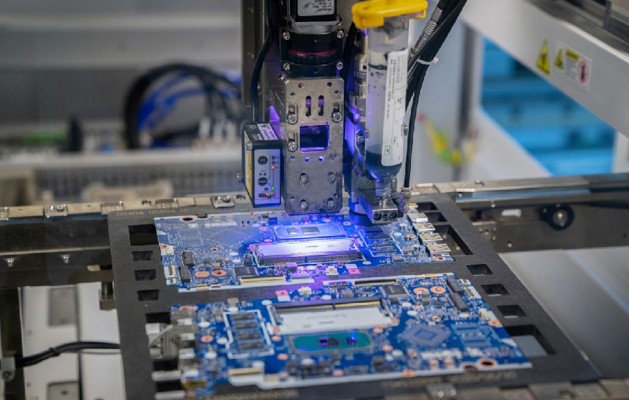
- Assembly process window definition
- Reflow profile validation, paste selection, stencil strategy, and rework rules.
- Essential for fine pitch and dense routing typical of PCBA assembly multilayer.
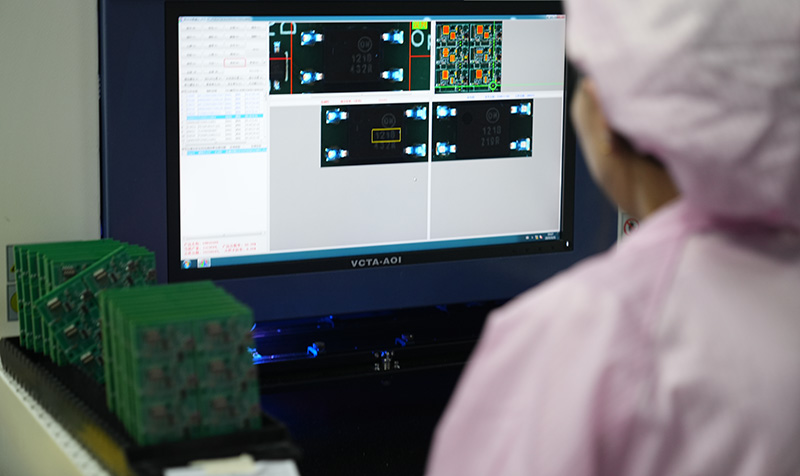
- Inspection and test gating
- AOI criteria aligned to IPC class; X-Ray for hidden joints.
- Clear pass/fail rules, not “operator judgment.”
- Traceability and change control
- Lot-level tracking for laminate, solder paste, and key components.
- DFM/DFT readiness
- Test point policy, boundary scan planning, and fixture feasibility.
Quick control checklist for medical builds
| Control Item | What You Want To See | Why It Builds Trust |
|---|---|---|
| Stack-up freeze | Signed build note + impedance table | Prevents “build drift” |
| Microsection plan | Defined coupons + sampling frequency | Verifies vias and dielectric |
| Assembly window | Profile + paste + stencil rules | Cuts BGA/QFN defects |
| Traceability | Lot mapping and records | Supports audits and RMAs |
In practice, multilayer PCBA stability comes from repeatable inputs and measurable checkpoints—not from last-minute inspections.
How Are Multilayer PCB PCBA Assembly Standards Applied In Medical And Automotive Manufacturing?
This section is about execution: standards only matter when they are translated into work instructions, acceptance criteria, and measurable records. Medical and automotive overlap on reliability culture, but medical electronics adds documentation expectations, controlled change management, and traceability intensity.
Where standards show up on the factory floor
- Acceptance criteria tied to IPC class
- Solder joint requirements, conductor spacing, annular ring, and cosmetic rules.
- Documented process instructions
- Paste handling, bake rules, moisture sensitivity, and rework limits.
- Inspection plans with defined escape-prevention
- AOI programming rules, X-Ray sampling logic, and manual inspection triggers.
- Test strategy aligned to risk
- ICT where coverage makes sense; FCT to validate functional intent.
- Traceability and deviation control
- Controlled records for component substitutions and process exceptions.
- Reliability-oriented verification
- Thermal cycling or stress screening where the product risk demands it.
Medical vs automotive execution focus
| Topic | Medical Electronics Focus | Automotive Electronics Focus |
|---|---|---|
| Documentation | Traceability + controlled deviations | Traceability + PPAP-style rigor |
| Change control | Tight, audit-friendly | Tight, high-volume resilience |
| Reliability targets | Patient safety and continuity | Harsh environment durability |
When you evaluate multilayer PCB PCBA assembly, look for proof of standards in records and checkpoints—not only certificates on a wall.
What Makes FR4 Multilayer PCB PCBA A Common Industry Choice?
For medical electronics, FR-4 is common because it balances electrical stability, manufacturability, and cost control across prototypes and volume builds—especially when the design is not strictly RF/microwave. A well-chosen FR-4 system supports consistent lamination, predictable drilling, and stable soldering behavior.
Why FR-4 keeps winning for many medical boards
- Broad supplier ecosystem in China for controlled quality builds.
- Predictable processing for lamination and drilled hole reliability.
- Cost-effective for iterations when you are still tuning firmware and sensors.
- Compatible with high-density routing in mainstream multilayer designs.
- Supports common finishes for reliable assembly and rework.
Where FR-4 is used most often in medical electronics
- Patient monitoring modules
- Control boards with mixed analog/digital signals
- Interface boards and connector-rich designs
- Compact power and communication boards
If your project includes FR4 multilayer PCB PCBA, the trust factor comes from specifying the right Tg, controlling resin flow, and maintaining consistent lamination results across lots.
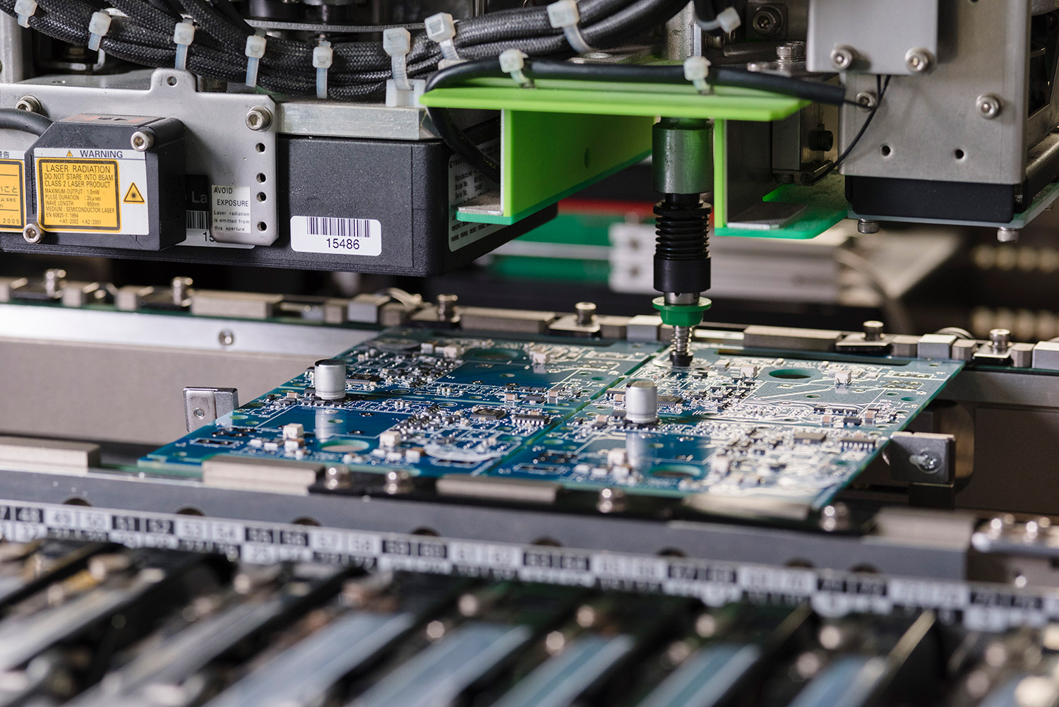
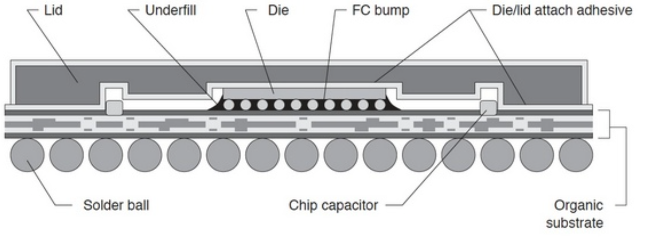
How Does Multilayer PCB Manufacturing Process Affect Final PCBA Quality?
Medical PCBA quality is “built in” during PCB fabrication, not rescued during assembly. The multilayer process controls how well vias survive cycling, how consistent impedance stays, and how stable the board behaves through reflow.
Manufacturing steps that most influence assembly yield
- Layer imaging and registration
- Misregistration steals annular ring margin and risks opens.
- Lamination quality
- Poor lamination increases delamination and CAF risk in harsh conditions.
- Drilling and desmear
- Smear control and wall prep drive plating adhesion.
- Electroless + electrolytic copper plating
- Defines via wall integrity and continuity over life.
- Solder mask definition
- Matters for fine pitch spacing and solder bridging control.
- Surface finish quality
- Impacts solder wetting, rework success, and long-term reliability.
- Electrical test strategy
- Nets verification reduces escapes before assembly.
A compact “process-to-risk” view
| Process Area | Typical Risk | What A Good Factory Does |
|---|---|---|
| Lamination | Delamination, voids | Controlled press recipe + coupons |
| Via formation | Intermittent opens | Microsection + plating window control |
| Mask/finish | Poor soldering | Tight mask alignment + finish QA |
| E-test | Escapes | 100% net test where appropriate |
For PCBA manufacturing multilayer, process transparency is a practical trust signal: you want measurable controls, not verbal assurances.
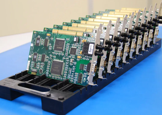
What Are Typical Use Cases For 6 Layers PCBA Multilayer PCB Designs?
A 6-layer build is often the “sweet spot” where you can separate noisy digital sections from sensitive analog, add solid reference planes, and still keep cost and lead time under control. In medical devices, this is especially useful for compact boards that include wireless, sensors, and regulated power.
Common 6-layer patterns in medical electronics
- Signal / Ground / Signal / Power / Ground / Signal
- High-speed + analog separation using dedicated reference planes
- Cleaner EMI behavior from continuous planes and controlled return paths
- Better routing efficiency around connectors and shielding constraints
- Improved power integrity with well-defined plane impedance
Typical products where 6-layer is practical
- Wearable and portable monitoring units
- Medical interface and communications modules
- Compact controller boards with motor/actuator interfaces
- Dense connector and isolation-heavy designs
If you are scoping 6 layers PCBA multilayer PCB, the decision should be driven by return path control, EMI margin, and routing congestion—not by layer count as a status symbol.
Where Are Multilayer PCB Application Scenarios Most Common Today?
Multilayer PCBs appear wherever systems are compact, feature-rich, and expected to run reliably over long duty cycles. In medical electronics, the drivers are miniaturization, low noise, and predictable behavior through assembly and rework.
High-frequency and specialty scenarios
While FR-4 covers a large share, certain designs call for specialty builds such as multilayer high frequency metal base PCB PCBA circuit boards when thermal and RF constraints dominate. These are less common in mainstream medical controls, but they matter in imaging, high-power modules, and RF front ends.
Common multilayer PCB application categories
- Medical monitoring and diagnostics (signal integrity + low noise)
- Industrial medical subsystems (robust interfaces)
- Automotive-adjacent medical modules (harsh environment tolerance)
- LED and indicator systems (where LED 94v0 FR4 multilayer PCBA may appear)
- EMS programs needing fast iteration (multilayer EMS PCBA)
- Prototype-to-production flows (rapid learning cycles)
“Application fit” is a trust builder when your manufacturer can map your use case to specific process controls and validation steps.
Why Choose EBest Circuit (Best Technology) as Your Reliable Multilayer PCBA Manufacturer In China?
For medical electronics, supplier selection is a risk decision: you need stable output, audit-friendly records, and the ability to handle complex builds without constant escalation. EBest Circuit (Best Technology) focuses on engineering-led manufacturing where build inputs are verified early and controlled throughout production.
What sets EBest Circuit (Best Technology) apart in medical multilayer PCBA manufacturing
- ISO 13485–Certified Quality System: Medical PCBA manufacturing governed by ISO 13485, with audit-ready documentation, controlled change management, and traceable production records.
- MES-Enabled Digital Workshop: A fully digitalized manufacturing environment powered by MES, enabling 5-second traceability across materials, PCBA serials, production cycles, and real-time production status.
- Engineering-Led DFM Pre-Review: Structured DFM analysis conducted by PCB and PCBA engineers with over 20 years of experience, delivering formal DFM reports, process-fit recommendations, and BOM optimization outputs.
- Prototype-to-Volume Continuity: Seamless scaling from prototype and pilot builds to volume production under the same quality system, MES framework, and engineering controls—without process resets or traceability gaps.
If you are sourcing China multilayer PCBA or evaluating a multilayer PCBA manufacturer, the most reliable indicator is how clearly the factory explains controls, records, and exception handling. For project evaluation and quoting, contact sales@bestpcbs.com.
In a nutshell, multilayer PCBA enables compact, reliable medical electronics by combining dense routing, stable reference planes, and robust interconnect structures that survive real-world assembly and operation. This article walked through the process risks and prevention methods, engineering controls, standards execution, FR-4 material rationale, manufacturing flow impacts, 6-layer use cases, and where multilayer designs fit best in medical systems. EBest Circuit (Best Technology) supports Multilayer PCBA Manufacturing in China for Medical Electronics with engineering-led controls, inspection discipline, and production-ready documentation. Contact sales@bestpcbs.com to discuss your stack-up, build requirements, and manufacturing plan.
FAQs
When to use multilayer PCB?
Use a multilayer PCB when routing congestion, EMI margin, power integrity, or controlled impedance requirements cannot be met on a double layer PCB without compromises that increase risk.
What does a 4 layer PCB mean?
A 4-layer PCB typically includes two outer signal layers and two inner layers used as ground and power planes, improving return paths, EMI control, and routing space versus a 2-layer board.
Is there a 3 layer PCB?
Yes, a 3-layer PCB can exist, but it is uncommon because symmetric stack-ups are preferred for lamination stability and warpage control; most designs move to 4 layers instead.
Can you have a 3 layer PCB?
You can, but it is usually a special-case decision; 4 layers is the more standard step up because it balances electrical performance and manufacturing stability.
What is a class 3 PCB?
Class 3 refers to the highest reliability level in IPC classification, typically used in products where continued performance is critical and defects are less tolerable than in Class 1 or Class 2.
What are the 7 types of PCB testing methods?
Common PCB/PCBA test methods include AOI, X-Ray inspection, electrical net test, ICT, flying probe test, functional test (FCT), and burn-in or stress screening (used when risk requires it).
What does a 2 layer PCB mean?
A 2-layer PCB has copper on the top and bottom only; it is cost-effective and fast, but it offers less routing space and weaker EMI/power integrity control compared with multilayer boards.