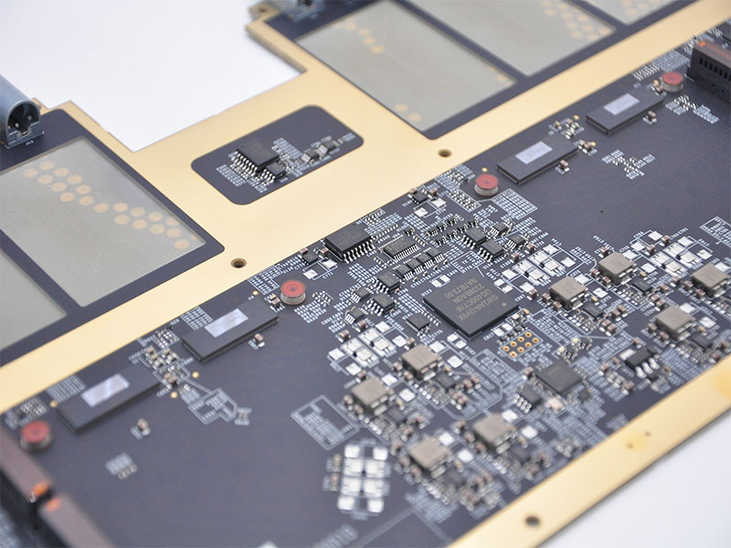
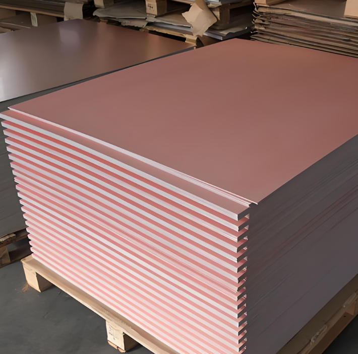
FR4 thermal conductivity is one of the most frequently misunderstood parameters in PCB thermal design. Although FR4 is the most widely used PCB substrate, its ability to conduct heat is inherently limited and must be compensated through copper design, vias, and system-level cooling.
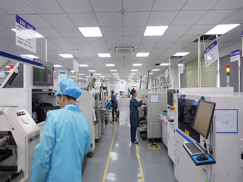
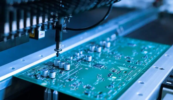
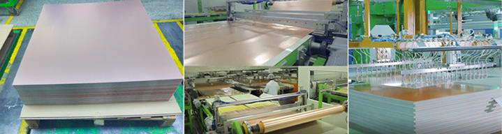
In real PCB projects, managing FR4 thermal conductivity is less about the material alone and more about how design and manufacturing decisions work together. EBest Circuit (Best Technology) addresses these limitations by providing fast, engineer-to-engineer support across material selection, stack-up design, and thermal path optimization. With DFM pre-review and BOM optimization led by PCB and PCBA engineers with over 20 years of experience, we help engineers design copper distribution, via structures, and layouts that compensate for FR4’s low thermal conductivity. For thermal design consultation or FR4-based PCB projects, please contact us at sales@bestpcbs.com.
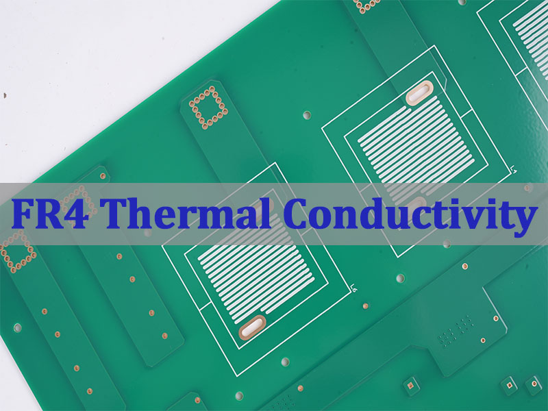
What Is FR4 Thermal Conductivity?
FR4 thermal conductivity describes how efficiently heat can pass through the glass-epoxy laminate used as the PCB substrate. Because FR4 is primarily composed of epoxy resin reinforced with glass fiber, it is mechanically strong and electrically insulating, but thermally inefficient.
From a design perspective, low FR4 thermal conductivity means:
- Heat tends to remain localized near heat sources
- Substrate alone cannot spread or dissipate power effectively
- Thermal paths must be intentionally engineered
This is why FR4 is suitable for signal integrity and structural stability, but not for direct heat spreading.
Typical FR4 Thermal Conductivity Values (W/m·K)
The thermal conductivity of FR4 is relatively consistent across suppliers, but small variations exist depending on resin formulation and glass content.
Typical reference values used in engineering calculations:
- FR4 thermal conductivity: 0.25–0.35 W/m·K
- Common design assumption: 0.3 W/m·K
This value is often expressed as FR4 thermal conductivity W/m·K in datasheets and simulation tools.
Compared to metals, this confirms that FR4 contributes very little to heat removal and should not be relied upon as a thermal path.
Thermal Conductivity of FR4 PCB vs Copper Layers
In an FR4 PCB, the substrate is not the primary heat conductor.
Copper thermal conductivity dominates thermal behavior.
Typical comparison:
- Copper: ~390–400 W/m·K
- FR4 epoxy: ~0.3 W/m·K
This difference of more than 1,000× explains why:
- Copper planes act as heat spreaders
- Copper thickness matters more than FR4 selection
- Thermal vias are essential for vertical heat transfer
In real designs, improving copper distribution yields far greater benefit than changing FR4 grade.
FR4 In-Plane vs Through-Plane Thermal Conductivity
FR4 does not conduct heat uniformly in all directions.
Its thermal conductivity is anisotropic.
- FR4 in-plane thermal conductivity: slightly higher due to glass fiber alignment
- FR4 through-plane thermal conductivity: lower due to resin-rich layers
This is why heat spreads laterally across copper planes more effectively than vertically through the board thickness.
For power components, vertical heat flow must be assisted using thermal vias and copper-filled structures.
FR4 Thermal Conductivity vs Temperature
FR4 thermal conductivity vs temperature remains relatively stable at moderate operating ranges, but degradation occurs as temperature increases.
As temperature rises:
- Epoxy resin softens
- Interfacial thermal resistance increases
- Effective heat transfer decreases
High-temperature operation close to Tg accelerates aging and can reduce long-term reliability, even if the nominal thermal conductivity value appears unchanged.
FR4 vs G10 Thermal Conductivity Comparison
FR4 and G10 are often compared due to similar composition.
From a thermal standpoint, the difference is minimal.
- Thermal conductivity of G10 FR4: ~0.3 W/m·K
- Practical PCB thermal behavior: essentially identical
Electrical and flame-retardant properties differ more than thermal performance.
Therefore, G10 FR4 thermal conductivity should be treated as equivalent for thermal calculations.
High Tg FR4 and Thermally Conductive FR4 Materials
High Tg FR4 is commonly misunderstood as a higher thermal conductivity material.
In reality, Tg affects thermal stability, not heat transfer.
Key distinctions:
- High Tg FR4 thermal conductivity: similar to standard FR4
- Tg improves resistance to thermal deformation, not heat flow
Special thermally conductive FR4 formulations exist and may reach 0.6–1.0 W/m·K, but they:
- Increase material cost
- Still fall far below metal or ceramic substrates
Such materials are niche solutions, not general replacements.
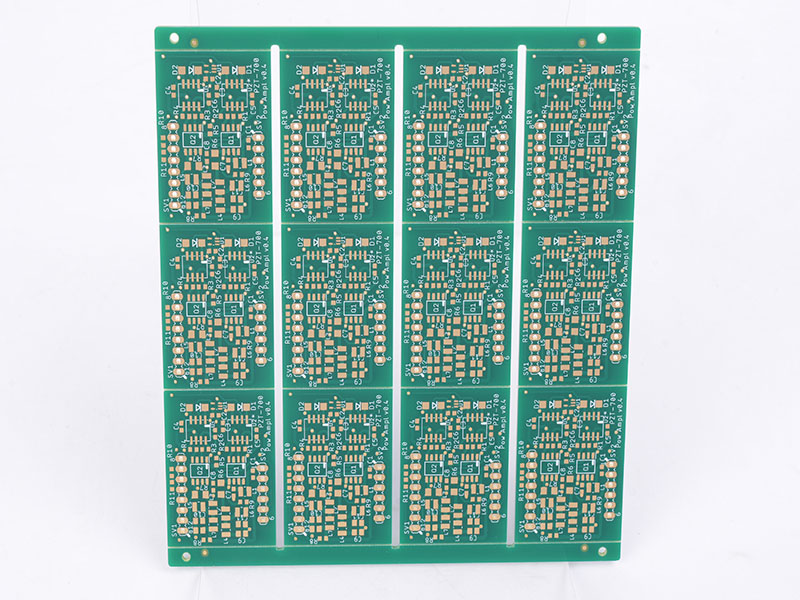
FR4 PCB Thermal Conductivity in Real Applications
In real-world electronics, FR4 PCB thermal conductivity rarely limits performance alone.
System-level design choices dominate.
FR4 performs well in:
- Digital logic boards
- Control electronics
- Low to medium power designs
Thermal failure typically results from layout constraints or enclosure limitations, not FR4 material selection.
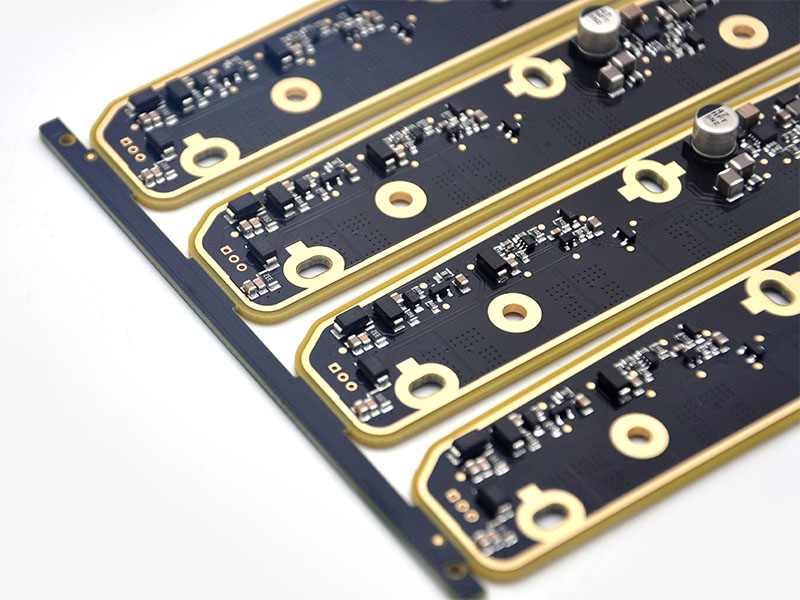
How to Improve Heat Dissipation on FR4 PCBs?
Because FR4 is thermally weak, engineers rely on structural solutions.
Common techniques include:
- Increasing copper weight
- Using continuous copper planes
- Adding dense thermal via arrays
- Coupling the PCB to metal housings or heatsinks
These approaches effectively bypass low FR4 board thermal conductivity.
FR4 Thermal Conductivity Calculator and Design Reference
A FR4 thermal conductivity calculator should be used with caution.
Material-only calculations often underestimate real temperatures.
Recommended design approach:
- Use 0.3 W/m·K for FR4
- Model copper separately
- Validate using thermal simulation or testing
This hybrid method yields results closer to actual operating conditions.
Cost Comparison: FR4 vs High Thermal Conductivity PCB Materials
FR4 remains dominant due to cost efficiency.
Relative comparison:
- FR4: lowest cost, lowest thermal conductivity
- Aluminum / ceramic: higher cost, high thermal conductivity
Unless power density demands it, upgrading material is rarely the most economical solution.
To sum up, this article explained FR4 thermal conductivity values, how heat flows in FR4 PCBs, and how engineers manage thermal performance through copper and design techniques.
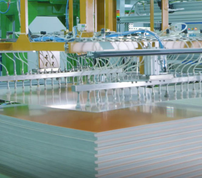
EBest Circuit (Best Technology) supports thermal-critical PCB projects through DFM-driven material selection and practical thermal design guidance provided by engineers with over 20 years of PCB experience, while delivering PCB fabrication and PCBA assembly through a fully integrated in-house process. With in-house PCB and PCBA factories, digital process traceability, and fast PCBA delivery as short as 1.5 weeks, we help engineering teams validate designs and move to production. If you need support selecting FR4 materials or designing for thermal performance, please contact us via sales@bestpcbs.com.
FAQ: FR4 Thermal Conductivity and PCB Material Questions
Is FR4 a good thermal insulator?
Yes. FR4 has low thermal conductivity and limits heat flow.
What is the thermal conductivity of a PCB board?
FR4 PCBs are typically around 0.3 W/m·K.
Which PCB material has high thermal conductivity?
Aluminum-based and ceramic substrates.
Is FR4 electrically conductive?
No. FR4 is electrically insulating.