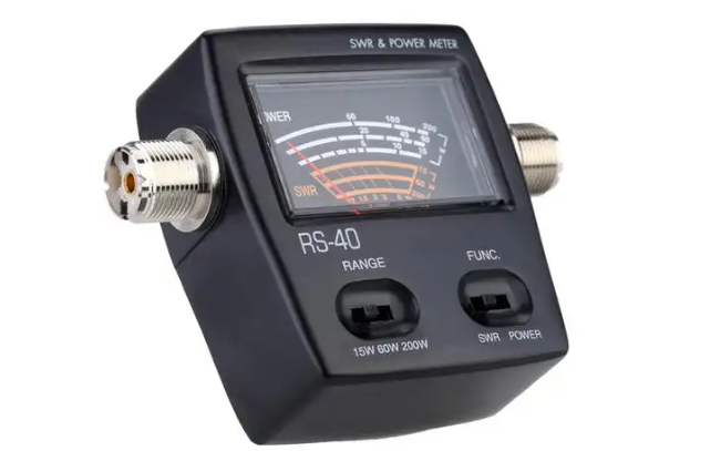
Standing Wave Ratio (SWR) power meters are essential for ensuring your radio equipment operates efficiently. These devices help users monitor power and maintain good transmission quality. Some wonder if diodes, common in various electronic circuits, can play a role in these meters. This article explores SWR power meters, their usage, and whether diodes can be used for this purpose.
What is an SWR Power Meter?
An SWR power meter measures the ratio of forward power to reflected power in a transmission line. This ratio helps determine how efficiently the transmitter’s power is delivered to the antenna. A good SWR ensures that most of the energy reaches the antenna, minimizing losses and protecting equipment.
An SWR value close to 1:1 indicates almost all power is transmitted with minimal reflection. Higher values show more power is bouncing back, which can lead to damage or poor performance.
How Does an SWR Power Meter Work?
SWR power meters are installed between the transmitter and the antenna. They measure forward power and reflected power. The forward power travels from the transmitter to the antenna, while reflected power is what returns due to impedance mismatches.
The meter calculates the SWR by comparing these two readings. Meters use directional couplers, sensitive enough to differentiate the power flows. The main goal is to ensure most energy travels forward with minimal loss.
How to Read an SWR Power Meter?
Reading an SWR meter is straightforward. Here’s how:
- Power On: Turn on the transmitter at low power.
- Set to Forward: Set the meter to the forward position and take note of the power.
- Switch to Reflect: Change the meter to read the reflected power.
- Check Ratio: Compare both readings to get the SWR.
A good reading is typically below 2:1. If it’s higher, adjustments to the antenna or transmission line may be needed.
How to Use an SWR Power Meter?
Using an SWR meter helps ensure you’re not wasting energy. Follow these steps:
Connect Properly: Place the meter between the transmitter and the antenna.
Select the Band: Choose the frequency you plan to transmit.
Adjust Power Levels: Start with lower power and increase as needed.
Read and Interpret: Note both forward and reflected power.
Adjustments can include changing the length of the transmission line or repositioning the antenna. These small tweaks help maintain a safe SWR level, ensuring longer equipment life.
Where Do You Put an SWR Meter?
Placement is critical for accurate SWR readings and maintaining optimal performance in your transmission setup. An SWR meter must be positioned directly between the transmitter and the antenna to accurately measure both the forward and reflected power.
Close to the Transmitter
Ideally, the SWR meter should be placed as close to the transmitter as possible. This ensures that any potential loss or reflection occurring within the cable before the meter is accounted for in the measurement. Keeping it close to the transmitter also reduces the risk of incorrect readings due to cable impedance variations.
Inline Connection
The SWR meter needs to be connected inline with the coaxial cable running from the transmitter to the antenna. Make sure to insert the meter so that the “Transmitter” or “TX” side of the meter is connected to the radio, and the “Antenna” or “ANT” side is connected to the feed line that goes to the antenna.
Ensure Firm Connections
A secure connection is essential to avoid power leaks or signal degradation. Loose or improperly connected cables can distort readings and give false impressions of your SWR levels.
Temporary vs. Permanent Placement
If you are conducting a one-time SWR check, a temporary connection may be enough. For continuous monitoring, you can install the meter as a permanent fixture in your transmission line. Permanent placement is particularly useful for setups where you frequently switch bands or adjust power levels and need constant feedback.
Minimize Cable Lengths
Extra cable between the transmitter and the SWR meter can introduce unwanted losses and impedance mismatches. Keeping the cable length minimal between the devices helps maintain the true characteristics of the transmission line, ensuring your SWR reading is as accurate as possible.
Environment Considerations
Place the SWR meter in a location that is easy to read and free from extreme temperature or humidity. Environmental factors can affect the meter’s internal components over time, leading to inaccuracies. Additionally, avoid areas with strong electromagnetic interference, as it can distort the meter’s readings.
Can a Diode Be Used as an SWR Power Meter?
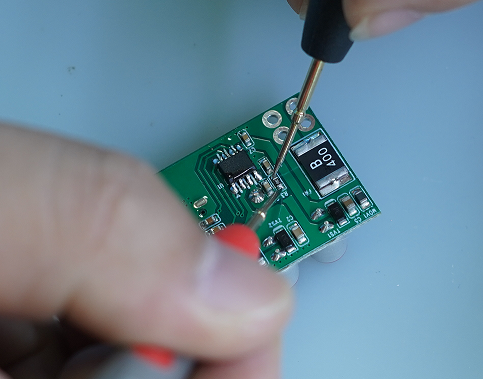
A diode can indeed play a part in an SWR power meter but not as the main measuring tool. Diodes are vital for rectifying alternating current (AC) into direct current (DC). In SWR meters, they detect voltage changes by converting RF signals into readable DC levels.
In simpler meters, diodes are part of the directional coupler circuit. This circuit separates forward and reflected signals. The diode’s role is to sense these signals and help display power levels. However, while they’re essential in detecting changes, diodes alone cannot fully replace an SWR power meter. They must work alongside other components for accurate results.
Do I Need a Diode on a Relay?
Relays switch circuits by opening and closing contacts. Sometimes, adding a diode across a relay’s coil is necessary. This type of diode, known as a flyback or snubber diode, protects against voltage spikes. When the relay is de-energized, the collapsing magnetic field can create high-voltage spikes. A diode helps by providing a path for the current, preventing damage to other parts.
In SWR meters, if relays are used to switch bands or paths, diodes could prevent potential damage. This adds safety to circuits, extending the life of the components.
How Do I Know if My SWR Meter Is Bad?
An SWR meter can fail over time. Here are signs that may indicate a problem:
Inconsistent Readings: If your meter shows fluctuating or unrealistic results, it could be faulty.
Zero Reflection: If the meter never shows any reflected power, even with known mismatches, it’s likely not functioning.
Physical Damage: Broken components or burnt circuits can lead to inaccurate readings.
Calibration Issues: A poorly calibrated meter may not reflect true power levels.
If you suspect a problem, testing the meter with known setups or professional recalibration might be necessary.
SWR power meters play a critical role in ensuring efficient power transmission. While diodes can be part of their design, they aren’t standalone SWR meters. Diodes help in detecting voltage changes, contributing to the overall accuracy of readings. Proper use and placement of an SWR meter ensure good transmission quality and equipment longevity. If you’re considering adding diodes to other components, such as relays, they can offer valuable protection.
Choose reliable SWR meters to safeguard your transmission setup and maintain optimal performance. If accuracy and durability matter, it’s worth investing in well-calibrated tools that use components like diodes effectively.