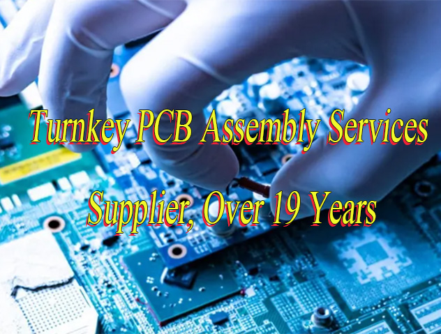
Turnkey PCB Assemblyrefers to a single supplier providing a complete service process, from design review and component procurement to PCB manufacturing, assembly, testing, and packaging. Customers only need to provide design files to receive a complete and usable finished circuit board. This model integrates supply chain resources, eliminating the complexity of coordinating multiple suppliers and achieving “plug-and-play” delivery.
Faster Time-to-Market: Cuts assembly time from 15-20 days to 7-10 days, supports 48-hour rapid prototyping for early market entry.
Technical Expertise: Free DFM consultations and advanced engineering support (signal integrity, EMI/EMC), solves design challenges upfront.
Scalable Production: Adapts from small batches to mass production, modular lines handle diverse PCB sizes/layers without capacity waste.
Transparent Tracking: Real-time project visibility via online systems, automated alerts and remote audits ensure accountability.
When to Use Turnkey PCB Assembly Services?
Applications of Turnkey PCB Assembly Service:
Rapid market feasibility verification for startups (48-hour rapid prototyping).
Small- to medium-volume production of 50-50,000 units (adaptable to modular production lines).
High-frequency, high-speed, HDI, rigid-flex PCBs, and other complex process projects.
Supply chain stability during periods of component shortages and price fluctuations.
Quality control scenarios requiring ISO13485/IATF16949 certification for medical and automotive electronics.
What Problems Turnkey PCB Assembly Can Solve?
Cost Efficiency Optimization: Turnkey PCB Assembly integrates design, procurement, manufacturing, and testing to reduce logistics, communication, and management costs. For example, bulk purchasing discounts and optimized inventory management cut single-board costs by 15–30% for overseas clients, especially small-batch production.
Time Acceleration & Market Responsiveness: Single-supplier coordination shortens prototype cycles from 4–6 weeks to 2–3 weeks, enabling rapid design-to-test closure. This helps overseas clients seize market opportunities in time-sensitive sectors like consumer electronics and medical devices.
Quality & Reliability Assurance: Expert teams control design specs, material selection, process parameters, and test standards, minimizing rework risks from design flaws or manufacturing errors. Techniques like AOI and X-ray inspection detect soldering defects early, ensuring compliance with standards (e.g., RoHS, UL) and boosting market trust.
Supply Chain Simplification & Risk Mitigation: Overseas clients avoid cross-border supplier coordination, time zone gaps, and language barriers. Turnkey providers manage the full chain from component sourcing to final assembly, preventing delays from shortages or logistics issues and ensuring stable material supply via global networks.
Flexible Production & Scalability: Supports elastic production from 10 prototypes to 10k+ volumes, eliminating frequent supplier changes. Startups can scale seamlessly from small-batch validation to mass production, reducing changeover costs and technical adaptation issues.
Technical Support & Optimization: Offers design optimization (e.g., PCB layout, thermal management), material guidance, and process improvements. Simulation tools predict design flaws, and cost-effective component alternatives enhance performance while cutting costs for overseas clients.
Risk Sharing & Compliance Guarantee: Providers assume liability for manufacturing defects and test failures, freeing clients from complex production issues. Familiarity with regulations (e.g., EU REACH, FCC) ensures compliance, reducing market entry barriers for overseas clients.
Turnkey Printed Circuit Board Assembly Process
1. Design and Verification: After customers submit design files (Gerber, BOM, component libraries), manufacturers conduct DFM (Design for Manufacturing) analysis. This includes checking layout rationality, compliance of line width/spacing (e.g., IPC-6012 standards), and thermal design optimization.
2. Material Procurement and Supply Chain Management: Based on the BOM, components and PCB substrates are procured from ISO 9001/14001 certified suppliers. An ERP system tracks material status to ensure traceability of critical components (e.g., BGA, CSP). Incoming materials undergo inspection, such as XRF testing for solder composition compliance.
3. PCB Manufacturing and Lamination: Processes include layer stacking, etching, drilling, and plating, adhering to standards like IPC-6013 (flexible boards) or IPC-6012 (rigid boards).
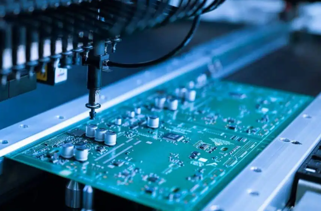
4. Surface Mount and Through-Hole Assembly: SMT production lines use high-speed placement machines (e.g., Siemens SIPLACE) for 0201 component placement with ±0.05mm accuracy. Through-hole components are assembled via wave soldering or selective soldering, combined with nitrogen protection to reduce oxidation.
5. Soldering and Connection Processes: Reflow soldering is performed in a nitrogen environment to ensure solder joint reliability and gloss. BGA packages undergo X-ray inspection for solder ball integrity. Soldering temperature profiles strictly follow J-STD-001 standards to prevent cold soldering or thermal damage.
6. Multidimensional Testing and Quality Inspection: In-line AOI detects placement deviations. ICT (In-Circuit Testing) verifies circuit functionality, while flying probe testing covers over 99% of network nodes. Functional testing simulates real-world conditions (e.g., -40°C to 125°C thermal shock), and aging tests last 168 hours to validate long-term stability.
7. Quality Control System: Visual inspections follow IPC-A-610 standards. SPC (Statistical Process Control) monitors critical parameters like solder paste thickness. Manufacturers certified under ISO 13485 (medical devices) or AS9100 (aerospace) implement additional environmental stress screening (e.g., vibration testing).
8. Packaging and Logistics: ESD-safe packaging (e.g., conductive foam) and vacuum-sealed moisture barriers are used. Logistics integrate tracking systems to ensure global delivery timeliness, such as 48-hour delivery via DHL/FedEx partnerships.
9. Final Validation and Delivery: Finished products undergo final functional testing, generating traceable batch reports (including test data and QC signatures). After customer confirmation, products enter mass production, supporting seamless transition from small-batch trials to large-scale manufacturing.
10. After-Sales Support and Feedback Loop: Technical documentation (e.g., assembly guides, troubleshooting manuals) and on-site support services are provided. Continuous process optimization is driven by customer feedback, such as implementing AI-powered defect prediction systems to reduce repair rates below 0.1%.
Turnkey PCB Assembly Types We Can Offer
Surface mount technology (SMT): High-precision placement machines enable automated placement of micro-components (such as 0201 packages and 0.35mm pitch BGAs), making it suitable for high-density, miniaturized circuit boards (such as smartphone motherboards).
Through-hole technology (THT): Wave soldering or hand soldering is used to mechanically secure and electrically connect large components (such as connectors and relays), making it suitable for applications requiring high mechanical strength (such as industrial power modules).
Hybrid technology (SMT/THT): Combining SMT and THT processes, it is compatible with both surface mount and plug-in components and is suitable for complex circuit designs (such as double-sided PCBs or multilayer boards).
Global Top-Tier Certification Quality Assurance System: Achieved ISO 9001, ISO 13485 (Medical), and AS9100D (Aerospace) triple international certifications, enforcing end-to-end rigorous control from raw material procurement to final delivery. Solder composition is 100% traceable, BGA solder ball integrity verified via X-ray NDT, with defect rates capped at 0.1%, significantly outperforming industry benchmarks.
Imported High-Speed SMT Mounting Capacity: Equipped with imported high-speed SMT machines, achieving ±0.05mm precision for 0201 components with 4 million SMT points/day + 3 million DIP points/day throughput. Supports seamless transition from small-batch (200PCS) prototyping to mass production (20K+), with standard lead time of 3 days and next-day express for urgent orders.
Lead-Free Soldering Process & Extreme Reliability Verification: Adopts J-STD-001-compliant lead-free solder paste process with 245-260℃ peak temperature control and ≥3℃/s cooling rate. Passes 168-hour thermal shock aging tests, enhancing solder joint gloss by 20% while maintaining cold solder rates below 0.1%.
Triple-Layer Inspection System for Full-Cycle Quality Control: AOI detects ±0.05mm placement deviations, ICT validates circuit functionality, and FCT simulates -40℃~125℃ extreme conditions. Flying probe tests cover 99% of net nodes with 99.9% signal integrity, ensuring zero-defect delivery.
MES-Enabled Full-Lifecycle Traceability: MES production execution system tracks material lifecycle with XRF composition testing and batch traceability for critical components. SPC monitors key parameters like solder paste thickness (±0.01mm), stabilizing yield at ≥98%.
Eco-Compliance & Cost Optimization: Complies with EU ROHS lead-free standards, reducing material costs by 10% through supply chain optimization. Combined with 85% full-line automation and high yield rates, overall project costs are 15% below industry averages.
ESD Protection & Global 48-Hour Logistics Network: Uses conductive foam + vacuum-sealed anti-static packaging. Integrates with DHL/FedEx for global 48-hour door-to-door delivery, supporting flexible multi-batch/small-quantity distribution.
Our Turnkey PCB Assembly Capabilities
Item
Capabilities
Placer Speed
13,200,000 chips/day
Bare Board Size
0.2″ × 0.2″ – 20″ × 20″ / 22″ × 47.5″
Minimum SMD Component
01005 (0.4mm × 0.2mm)
Minimum BGA Pitch
0.25mm (10mil)
Maximum Components
50mm × 150mm (Board Area)
Assembly Type
SMT / THT / Mixed Assembly
Component Package
Reels / Cut Tape / Tube / Tray / Loose Parts
Lead Time
1 – 5 days (Standard)
How to Get a Quote for Turnkey PCB Assembly Services?
Quotation Submission List for Turnkey PCB Assembly Services:
BOM (Bill of Materials): Excel/.xlsx/.csv, detailing component name, model, quantity, package type (SMT/THT), supplier, and specifications (e.g., 0603 resistor, SOP-8 package).
Gerber Design Files: Copper layer, solder mask layer, silkscreen layer, solder paste layer, and NC drill files in RS-274X format.
Centroid File (Pick-and-Place Coordinate File): Component coordinates, rotation angles, and reference designators for SMT machine programming and process validation.
PCB Engineering Drawings & Design Documents: Schematics, PCB layout diagrams, assembly drawings, and 3D models (e.g., STEP files) to specify hole positions, dimensions, connector placements, and special assembly requirements (e.g., waterproof coating, thermal design).
Testing & Certification Requirements: Test Specifications: ICT (In-Circuit Test), FCT (Functional Circuit Test), burn-in testing, X-ray inspection (for BGA/CSP), etc.
Certification Documents: RoHS, CCC, ISO, and other environmental/safety compliance requirements; specify lead-free process compliance.
Production Quantity & Lead Time: Define order quantities (e.g., small batch: 10-500pcs; bulk: 500+pcs) and delivery timelines (e.g., 8-48 hours for rapid prototyping, 1-2 weeks for mass production), which directly influence cost structure and production scheduling.
Welcome to contact us if you have any request for turnkey PCB assembly: sales@bestpcbs.com.
The printed circuit board production process is the fundamental sequence of steps that brings electronic designs to life. Understanding this process is key to appreciating the engineering behind the devices we use daily. This article will walk you through each stage, explain the importance of materials, and show how quality is guaranteed from start to finish.
Have you ever wondered what separates a high-performance, reliable PCB from one that fails prematurely? Are you struggling with:
Inconsistent quality from one production batch to the next?
Confusing communication and a lack of technical support from your supplier?
Delays in delivery that disrupt your own production schedules?
Hidden costs that appear after you’ve placed an order?
Limited capabilities in a supplier, preventing you from exploring advanced designs?
At EBest Circuit (Best Technology), we’ve built our entire operation around solving these exact problems. We provide:
A rigorous, data-driven quality control system that ensures every board, every time, meets spec.
Direct access to experienced engineers who speak your language and understand your challenges.
A streamlined production flow managed by advanced MES and ERP systems for on-time delivery.
Upfront, transparent pricing with no surprises, allowing for accurate budgeting.
A one-stop solution from basic FR4 boards to complex HDI, flex, and rigid-flex PCBs.
EBest Circuit (Best Technology) is a specialized PCB manufacturer with a modern, highly automated facility in China. Our team of seasoned engineers leverages cutting-edge technology to deliver great quality boards. We pride ourselves on being a reliable extension of your engineering team. For a consultation on your next project, reach out to us at sales@bestpcbs.com.
What Is the Printed Circuit Board Production Process?
The printed circuit board production process is the methodical series of steps used to manufacture the essential electrical pathways that connect components in electronic devices.
At its core, the process is about creating order out of raw materials. It involves precisely patterning conductive pathways onto insulating substrates, connecting multiple layers with microscopic precision, and protecting the circuit from environmental challenges. Understanding this flow is crucial for any engineer or purchaser, as it highlights the critical control points that separate a good board from a great one.
At EBest Circuit (Best Technology), we see this process as our core expertise, not just a series of steps. Our approach is built on a foundation of three key principles:
Precision Engineering: We go beyond basic specifications. For instance, our drilling capabilities can achieve hole diameters as small as 0.1mm with positional accuracy of ±0.025mm, ensuring perfect alignment for even the most dense designs.
Controlled Automation: Our factory floor features fully automated optical inspection (AOI) systems that scan every layer for defects invisible to the human eye. This isn’t just about efficiency; it’s about eliminating human error and guaranteeing consistency across every production panel, from the first board to the thousandth.
Proactive Collaboration: The process starts long before production. Our engineering team conducts a thorough Design for Manufacturability (DFM) analysis on every order. We don’t just build your design; we partner with you to identify potential issues like acid traps or insufficient copper balancing upfront, saving time and cost by preventing failures before they happen.
This meticulous attention to detail at every stage—from material selection and chemical processing to final electrical testing—is what defines our printed circuit board fabrication process flow. It’s how we ensure that every board leaving our facility not only meets the print but is built to exceed expectations, fully embodying our commitment to quality that is “Made in China, Trusted Worldwide.”
Printed Circuit Board Production Process – EBest Circuit (Best Technology)
At EBest Circuit (Best Technology), we understand that high-frequency PCB manufacturing requires specialized expertise. While standard FR-4 boards follow conventional workflows, PTFE-based high-frequency materials demand precise process adaptations. Here’s how we handle different high-frequency board scenarios:
A. NPTH PTFE Boards: Streamlined for Simplicity
For non-plated-through-hole PTFE applications, we employ an optimized process:
Panel Preparation: Precision cutting of PTFE laminates
Drilling: Creating component holes with PTFE-optimized parameters
Circuit Patterning: Direct imaging and pattern transfer
Etching: Precise copper removal to define circuits
AOI Inspection: Automated optical verification
Solder Mask Application: Protection with high-frequency compatible materials
Outer Layer Processing: Pattern transfer and plating
Final Processing: Completion through standard workflow
Key Differentiators for High-Frequency Success:
Material-Specific Expertise: Each material family receives customized processing parameters
Process Optimization: Critical adjustments at drilling, plating, solder mask, and routing stages
Quality Assurance: Enhanced inspection protocols at each manufacturing stage
Technical Flexibility: Ability to handle pure PTFE, ceramic hydrocarbon, and hybrid constructions
Our manufacturing approach ensures that whether you require simple NPTH designs or complex multilayer high-frequency boards, each product receives the specialized attention necessary for optimal RF performance. The careful process adaptations for PTFE materials—particularly in drilling, hole preparation, and plating stages—make the crucial difference in achieving consistent high-frequency performance.
By maintaining strict process controls and material-specific expertise, we deliver high-frequency PCBs that meet the most demanding performance specifications while ensuring manufacturing reliability and consistency.
Material Matters: Why We Choose the Right Base for Every Application
Think of your PCB’s substrate as the foundation of a building. A weak or unsuitable foundation will compromise the entire structure, no matter how perfect the design. The base material is not just a passive platform; it actively dictates your board’s electrical performance, thermal resilience, mechanical strength, and ultimate reliability. Choosing the wrong material is a primary reason behind field failures, signal integrity issues, and manufacturing defects.
At EBest Circuit (Best Technology), we go beyond simply sourcing laminates from top global suppliers. Our engineering team acts as your guide, translating complex material properties into practical solutions for your specific application. We help you navigate the critical trade-offs between performance, cost, and manufacturability.
1. FR-4
FR-4 remains the industry standard for a vast range of applications due to its excellent balance of properties and cost-effectiveness.
What It Is: A composite material made from woven fiberglass cloth and an epoxy resin binder.
Key Considerations: The critical differentiator within FR-4 is its Glass Transition Temperature (Tg). Think of Tg as the temperature at which the solid substrate begins to soften. Standard FR-4 has a Tg around 130-140°C, which is sufficient for conventional soldering processes.
When to Choose High-Tg FR-4: For lead-free soldering (which requires higher temperatures) or applications in elevated temperature environments (like under-hood automotive electronics), High-Tg FR-4 (≥170°C) is essential. It provides superior thermal stability, preventing board deformation (delamination) and ensuring long-term reliability. We also pay close attention to the Td value (Decomposition Temperature); a higher Td (e.g., >350°C) means better resistance to thermal breakdown during repeated thermal cycles.
2. High-Speed Materials
When your design involves high-frequency signals, standard FR-4 can cause significant signal degradation. This is where specialized high-speed materials come in.
The Core Parameters: The two most critical properties are Dielectric Constant (Dk or Er) and Dissipation Factor (Df).
Dk influences the speed of your signals. A stable, low Dk value ensures consistent signal timing and controlled impedance.
Df measures the signal energy lost as heat. A lower Df (e.g., 0.003 vs. FR-4’s 0.020) is crucial for minimizing loss in high-speed digital applications (like servers, networking gear) and RF circuits.
Our Approach: We recommend materials like ISOLA’s FR408HR or Panasonic’s Megtron series when signal integrity is paramount. These materials offer tight Dk/Df tolerances and consistency across the panel, which is vital for impedance control.
3. High-Frequency Materials: Engineered for RF & Microwave
For applications pushing into the GHz range (e.g., radar, satellite communications, 5G infrastructure), PTFE-based materials (like Rogers RO4000® series) are the gold standard.
Why PTFE? These materials exhibit exceptionally low and stable Dk/Df values, enabling minimal signal loss and phase stability at microwave frequencies. However, they require specialized plasma treatment during manufacturing to ensure proper hole wall preparation for reliable plating—a process we have mastered.
Hybrid Constructions: We expertly manufacture multilayer boards that combine PTFE layers with ceramic-filled hydrocarbon thermoset materials (e.g., RO4350B), optimizing performance and cost.
4. Specialized Substrates for Demanding Applications
Metal-Core PCBs (Aluminum/Copper): When heat dissipation is the primary concern—such as in high-power LED lighting, power supplies, and automotive modules—metal-core boards are ideal. The metal base acts as an integrated heatsink, efficiently drawing heat away from critical components.
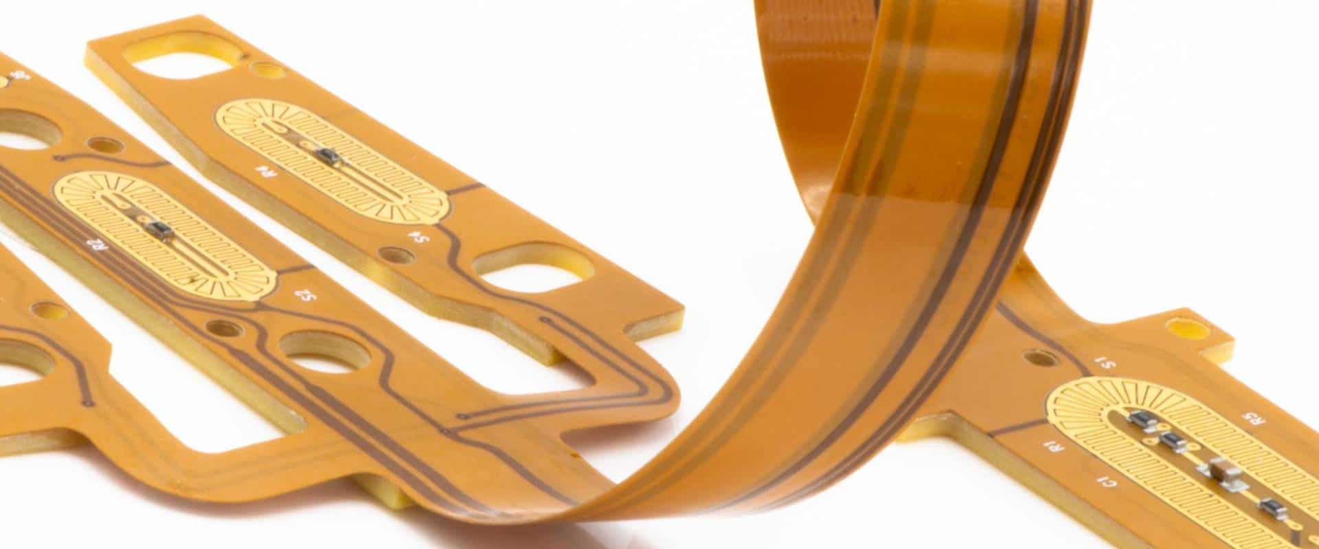
Flexible Materials (Polyimide): For products that need to bend, fold, or fit into compact spaces (wearables, medical devices, consumer electronics), flexible PCBs made from polyimide offer incredible durability, light weight, and excellent heat resistance.
In summary, understanding how are printed circuit boards made to meet your specific needs starts with selecting the right material. It’s a decision that impacts everything from electrical performance to manufacturing yield. Our engineers are here to demystify the data—from Tg and Td to Dk and Df—and help you select the optimal material that ensures your product’s success without over-engineering the cost.
How EBest Circuit (Best Technology) Ensures Consistent Quality in Every PCB?
Precision in manufacturing is useless without consistent quality. For us, quality is not just a final inspection step. It is a mindset integrated into every stage of our printed circuit board production. We are a precision-focused partner, not just a production shop.
Our commitment is backed by international certifications, including ISO9001, IATF16949 for automotive, ISO13485 for medical, and AS9100D for aerospace. Our inspection methods are robust:
Automated Optical Inspection (AOI): This system scans the boards to detect common flaws like scratches, stains, or incorrect parts.
Flying Probe Testing: This is a critical electrical test. It checks for short and open circuits on the bare board, ensuring the netlist matches the design.
Impedance Control: For high-speed designs, controlling the impedance of traces is vital. We test samples to ensure the impedance values are within your specified tolerance.
Cross-Section Analysis: We regularly cut sample boards to microscopically inspect the internal layers, plating thickness, and hole wall quality.
This systematic approach eliminates guesswork. It gives you data-driven confidence in the boards you receive.
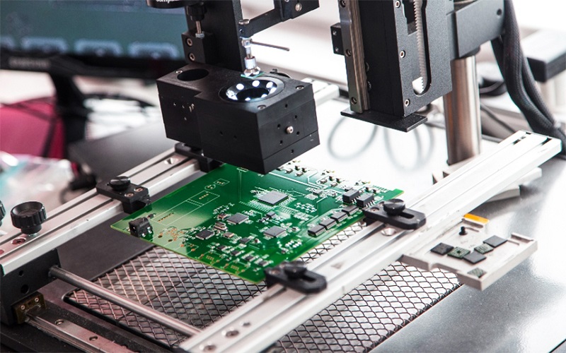
PCB Assembly Process: From Bare Board to Functional Circuit
EBest Circuit (Best Technology) has our own SMT factories in China and in Vietnam respectively. Here is our Core Flow of PCB Assembly: Incoming Materials (BGA/PCB) → Baking → Solder Paste → Printing → SPI → Component Placement → Reflow Soldering → Line Clearance → Post-Reflow Inspection → AOI → X-Ray → Through-Hole Insertion (THT) → Cleaning → Programming/Testing → Conformal Coating → Potting → Final Assembly → Labeling → Depaneling → Packaging & Shipping
Detailed Process Breakdown:
Incoming Materials (BGA/PCB)
Receipt and verification of customer-supplied PCBs and components (reel, tray, tube, or bulk).
Initial audit of documentation: BOM, centroid data (pick-and-place coordinates), and solder paste stencil design.
Baking
Purpose: To remove moisture absorbed by moisture-sensitive components and PCB substrates, preventing delamination, popcorning, or soldering defects during reflow.
Specifications:
All FPCs, sensitive ICs, and LEDs must be baked before production.
Standard ICs: 120°C for 12 hours.
LEDs (Tape & Reel): 60°C for 12 hours.
FPCs / FR-4 PCBs: 120°C for 1.5 hours.
Storage: Moisture-sensitive materials baked but not used on the same day are stored in controlled dry cabinets.
Solder Paste Management
Primary Alloy: We recommend and primarily use high-temperature solder paste.
Stencil Types: Standard, Step-up/Step-down, and Nano-coated (reduces paste adherence to apertures, improving print quality).
Common Sizes: 42x52cm (most common), up to 73.6×73.6cm.
Thickness: Ranges from 0.08mm to 0.15mm, determining solder paste volume. Aperture size is typically 10-20% larger than the pad.
Stencil Life: A stencil is retired if its tension measures ≤25N/cm² or after approximately 50,000 prints. Client-owned stencils are archived for three years.
Equipment: High-precision automated printers (e.g., GKG) with accuracy up to ±0.025mm.
Small PCB Support: PCBs smaller than the printer’s minimum size require a custom carrier fixture.
Solder Paste Inspection (SPI)
A 3D optical system inspects the paste printing quality immediately after the printer.
Measures: Paste volume, area, height, and alignment to detect defects like bridging, insufficient solder, or misplacement. Inspection precision is 10µm.
Automated Component Placement
Equipment: 4 SMT lines (2 Juki, 2 Yamaha YSM20R). The Yamaha YSM20R offers high-speed placement of up to 95,000 components per hour with an accuracy of ±0.035mm, supporting 0201 metric chip components.
Programming Requirements: BOM, centroid data, and board CAD data (for footprint verification).
Process: Components are picked from feeders using vacuum nozzles and placed with high precision.
Reflow Soldering
The PCB passes through a controlled thermal profile to melt the solder paste, forming permanent solder joints.
Reflow Options:
Nitrogen (N₂) Reflow: Soldering in an oxygen-free environment results in brighter, more reliable solder joints with significantly reduced oxidation and up to 10% fewer voids. This is our premium quality process.
Air Reflow: Standard process for many applications.
Process Control: Thermal profiles are meticulously monitored and recorded using profiling equipment to ensure they meet the specific requirements of the solder paste (e.g., peak temp ~220-245°C for high-temperature paste). Typical cycle time is 7-8 minutes.
Line Clearance & Post-Reflow Inspection
Line Clearance: Verification and accounting of all materials used in the production batch.
Post-Reflow Inspection: Initial manual visual inspection for gross defects like misplaced or tombstoned components, poor solder wetting, or board discoloration.
Automated Optical Inspection (AOI)
A high-speed camera system performs a comprehensive 2D/3D inspection of the assembled board.
Detects: Missing, misaligned, wrong, or damaged components; soldering defects like bridging, insufficient solder, and lifted leads.
X-Ray Inspection (AXI)
Purpose: To inspect hidden solder connections, such as those on Ball Grid Arrays (BGAs) and other bottom-termination components.
Rule: This step is mandatory for assemblies containing BGAs or any components with hidden joints.
Quality Standard: We adhere to an industry-standard voiding ratio of <25% for general electronics, with <10% achievable for automotive/medical-grade applications.
Through-Hole Technology (THT) / Manual Assembly
Process: Insertion and soldering of pin-in-hole components.
Equipment: Selective soldering machines are used for high-reliability applications, supporting PCBs up to 300x350mm with a placement accuracy of ±0.05mm.
Tools: ESD-safe soldering stations, solder wire, and appropriate PPE (mask, gloves).
Cleaning
Removal of flux residues and other contaminants post-soldering using approved solvents (e.g., alcohol, flux remover) or advanced methods like dry ice blasting. All chemicals are stored in flammable safety cabinets.
Programming & Functional Testing
Programming: In-circuit programming of MCUs, memory, etc., using customer-supplied firmware files.
Testing: Basic power-up and functional validation to ensure the PCBA operates as intended.
Conformal Coating & Potting
Conformal Coating: Application of a protective dielectric layer (Model: HS-6001) to shield the assembly from moisture, chemicals, and contamination. Typical thickness is 0.03mm. A UV tracer aids in inspection.
Potting/Encapsulation: Applying epoxy or silicone for additional mechanical strength and environmental protection.
Final Assembly → Labeling → Depaneling
Integration of the PCBA into its final enclosure or with other sub-assemblies.
Application of identification labels.
Separation of individual boards from a production panel (if applicable).
Packaging & Shipping
Packaging Solutions: ESD-safe packaging is used to prevent damage in transit, including anti-static bags, custom divider cards (cardboard or plastic), bubble wrap, and vacuum-formed trays.
In brief, this optimized SMT process flow, from meticulous material preparation to final packaging, ensures the manufacture of high-quality and reliable printed circuit board assemblies (PCBAs). By integrating precision machinery, strict process controls, and comprehensive inspection at every stage, we guarantee exceptional soldering quality, component reliability, and final product performance. This end-to-end control under one roof provides our clients with a streamlined, efficient, and accountable manufacturing solution.
Why Global Clients Choose EBest Circuit (Best Technology) for PCB Manufacturing
Our technical capabilities are only part of the story. The real value we provide comes from our partnership approach. We understand that you need more than just boards; you need a reliable solution that helps your business succeed.
Clients choose us for several key reasons:
Proven Results: We have helped companies across industries—from automotive to medical—reduce their production costs, improve delivery speed, and achieve higher quality outcomes.
Flexible Scale: We expertly handle everything from small-batch prototyping to high-volume mass production. This supports you from the R&D phase through to market launch.
Strong Technical Support: Our engineers are available to discuss design challenges, material selection, and any technical questions you may have. We are here to help you innovate.
Our commitment is to be more than a supplier. We aim to be a trusted partner in your success. The positive feedback we receive is a testament to this commitment.
Case of Printed Circuit Board Production by EBest Circuit (Best Technology)
In precision electronics manufacturing, maintaining optimal environmental conditions is critical for product quality and equipment longevity. By integrating Filter Monitoring system, manufacturers can achieve predictive maintenance of ventilation systems through real-time data collection and intelligent analysis. The system employs wireless sensors to track filter pressure differentials, temperature, and humidity, transmitting data via the LoRa network to a cloud platform for automated alerts and maintenance scheduling.
Key Application Scenarios
Energy Efficiency Optimization
Dynamic filter replacement cycles reduce fan energy consumption by over 15%.
Real-time alerts prevent equipment overheating due to filter blockages.
Example notification: “Eastern zone filter pressure threshold exceeded. Recommend replacement within 3 days.”
Cost Reduction
Eliminates manual inspections, cutting labor costs by up to 70%.
Precise monitoring avoids premature filter changes, reducing annual spare part costs by ~30%.
Risk Mitigation
Instant leakage or clog detection triggers multi-level alerts (SMS/email/phone).
Potential production disruptions are addressed within 24 hours.
Data-Driven Insights
Predictive algorithms forecast filter lifespan and seasonal contamination trends.
Customizable dashboards support compliance with ISO 50001 energy standards.
Printed Circuit Board Examples
Special Processes: Blind/Buried Vias, Impedance Control (±10%), Signal Loss <0.2dB/inch
LED Lighting: Heat dissipation management for high-power fixtures
For scenario-specific customization or demo data, please provide detailed requirements for further optimization.
Overall, the printed circuit board production process is a sophisticated dance of engineering and technology. It is the critical path that turns a design into a reality. Understanding this process helps in selecting the right manufacturing partner. This article has outlined the key stages, from material choice to final testing.
EBest Circuit (Best Technology) stands ready to be that partner for you. We combine advanced technology with deep expertise to deliver PCBs you can depend on. Our focus on quality, transparency, and partnership ensures your projects are in the best possible hands. Pls feel free to contact our team at sales@bestpcbs.com for a prompt and professional response.
FAQs
Q1: Why are tooling rails (process edges) necessary on PCBs?
Tooling rails are blank strips added along the edges of a PCB panel to provide space for automated SMT equipment to grip and transport the board during assembly. They also accommodate fiducial markers and tooling holes essential for accurate component placement. The standard width ranges from 5mm to 8mm.
Q2: Do you provide detailed production progress tracking?
Yes. We maintain a real-time Work-in-Progress (WIP) system that tracks each board’s status daily. Clients receive updates at key stages—from material preparation to final inspection—ensuring full transparency throughout production.
Q3: Which file formats do you accept for manufacturing?
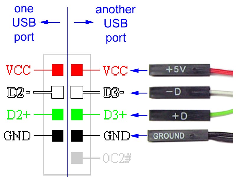
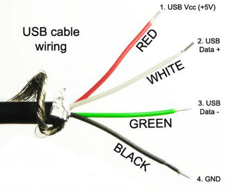
We support standard design formats including Gerber files (RS-274X), CAD data, and IPC-2581. For assembly, we require a Bill of Materials (BOM) and centroid (pick-and-place) files.
Q4: What is solder mask, and what is its function?
Solder mask is a protective polymer layer applied over copper traces to prevent oxidation, avoid solder bridges, and insulate circuits. It ensures solder adheres only to exposed pads (e.g., component leads and vias), improving reliability.
Q5: What solder mask colors are available?
We offer green, blue, black, red, white, yellow, and purple. Green is standard; other colors may involve longer lead times.
Q6: How long does SMT assembly take?
If components are in stock, SMT requires 2–3 days, followed by 1–2 days for testing. Most orders can be shipped within one week after production begins. Complex designs or special materials may extend the timeline.
For further details or project-specific queries, contact us at sales@bestpcbs.com.
HDI PCB manufacturing is a specialized process that pushes the boundaries of electronics design. It allows for the creation of incredibly complex and powerful devices that fit in the palm of your hand. This blog explains the process, benefits, and how to choose the right manufacturer for your advanced projects.
Are you battling with signal integrity issues in your HDI PCB designs? Many engineers and product managers face these exact challenges when pushing their PCB HDI technology forward.
Difficulty achieving high component density in a limited board space.
Signal loss and interference in complex, high-speed designs.
Managing heat dissipation in increasingly powerful but compact devices.
Facing high costs and long lead times for sophisticated multi-layer boards.
Finding a manufacturer with the right expertise and technology to bring an advanced design to life.
The good news is that these challenges have right solutions. By partnering with a skilled manufacturer, you can overcome these obstacles. Here is how a professional HDI PCB manufacturer addresses these points:
Utilizing microvias and stacked vias to maximize routing density in a small area.
Implementing precise impedance control and advanced materials to ensure clean signal transmission.
Offering specialized materials and thermal management techniques to keep your device running cool.
Providing cost-effective manufacturing strategies and reliable quick-turn services to meet your timeline and budget.
Bringing years of specialized experience and state-of-the-art equipment like laser drilling machines to the table.
BEST Technology is a professional HDI PCB manufacturing factory focused on delivering high-quality, high-density interconnect solutions. Our team is dedicated to supporting your projects from the initial design review to final assembly. For a personal consultation, pls feel free to reach out to us at sales@bestpcbs.com.
What Is HDI PCB Manufacturing?
At its heart, HDI PCB manufacturing is all about packing more functionality into a smaller space. It’s the advanced process of creating printed circuit boards with a significantly higher wiring density per unit area than conventional PCBs. Think of it as the difference between a wide, sprawling suburban neighborhood and a dense, efficient city skyline—both serve a purpose, but one is built for maximum space efficiency and interconnection.
To truly grasp the HDI PCB meaning, it’s helpful to understand its key building blocks:
1. Microvias, Blind, Buried and Through Vias: These are the tiny, laser-drilled holes that make HDI possible.
Microvias are incredibly small holes, typically with a diameter of less than 0.15mm. They act as miniature tunnels connecting adjacent layers.
Blind Vias connect an outer layer to an inner layer, but don’t go all the way through the board.
Buried Vias connect inner layers only, remaining hidden within the board’s core.
Through-holes refer to a hole that is open on both outer layers of a PCB, thereby connecting the two sides. This term encompasses via holes, plated through-holes (PTH), and non-plated through-holes (NPTH).
Why they matter: By using these small, targeted vias instead of large through-holes, designers can save a tremendous amount of space. This freed-up real estate allows for more components and more complex routing.
2. The Evolution to UHDI (Ultra High Density Interconnect): As technology pushes for even greater miniaturization, UHDI represents the next frontier. It involves even finer lines, smaller vias, and more advanced materials. If HDI is a dense city, UHDI is a city of micro-skyscrapers.
3. The Role of a Specialized HDI PCB Manufacturer: Not every factory can produce these advanced boards. A specialized HDI PCB manufacturer invests in specific technology—like laser drilling systems—and cultivates the expertise needed to manage the complex, sequential lamination processes involved. Choosing the right partner is crucial for success.
To truly understand what HDI PCBs are, let’s look at their key characteristics:
Key Features of HDI Technology:
Uses laser drilling instead of mechanical drilling, with via diameters ≤0.15mm
Microvias with bottom pads smaller than 0.25mm (10mil)
Fine line width/spacing of 3/3mil or less
Requires copper plating thickness ≥15μm in laser vias
Aspect ratio (dielectric thickness to via diameter) ≤1:1
How HDI Differs from Standard PCBs:
Contains blind vias, buried vias, or both
Requires multiple lamination cycles (≥2 times)
Involves multiple drilling and plating processes
Features much denser routing on both inner and outer layers
Has more complex manufacturing process and longer production cycles
In short, HDI PCB manufacturing is the enabling technology behind the powerful, compact electronics we rely on every day.
What Are the Types of HDI PCB Manufacturing Products?
The world of HDI is diverse, offering solutions for many different applications. The types of products are primarily classified by their layer buildup structure, which refers to the number of sequential lamination cycles and the arrangement of microvias. Understanding these structures is key to selecting the right board for your project.
A crucial concept here is the “order” or “step” of an HDI board, often described by formulas like a+N+a or a+N+N+a.
a stands for the Build-up layer, which is formed using laser microvias. Each additional build-up layer on one side counts as one “step” or “order”.
N stands for the Core layer, which is a traditional multilayer PCB with through-holes or buried vias. The value of N indicates the number of conductive layers within the core. For example, a 4-layer core is N=2 (counting internal layers), and an 8-layer core is N=4. This explains why “N” is often an even number.
Here is a clear outline of common HDI structures, from simple to complex:
1. 1+N+1 (1-Step HDI)
This is the simplest form of HDI. It features a single build-up of high-density interconnection layers on both sides of a core. This is a cost-effective entry point for adding HDI features, allowing for finer lines and microvias while keeping the process relatively straightforward.
2. 2+N+2 (2-Step HDI)
This structure involves two sequential HDI build-ups on each side. This allows for the use of stacked microvias (microvias placed directly on top of each other) or staggered microvias. It is ideal for designs requiring higher pin-count components and much greater routing density.
3. 3+N+3 and Beyond (3-Step / Any-layer HDI)
These are the most complex and advanced boards. They feature three or more sequential laminations, enabling “any-layer” interconnection, where virtually any layer in the board can be interconnected with microvias. This enables incredibly high component density and is used in cutting-edge applications like flagship smartphones, network servers, and medical imaging equipment.
HDI vs. Mechanical Blind/Buried Vias
It’s important to distinguish between laser-drilled HDI microvias and mechanically drilled blind/buried vias, as they represent different product types with distinct cost and capability profiles.
HDI (Laser Drilled):
Microvia Aperture: ≤ 0.15mm.
Characteristics: Uses laser drilling for high positioning accuracy, enabling very small apertures. Employs RCC (Resin Coated Copper) or laser-specific prepreg as dielectric material.
Applications: High-end miniaturized products.
Mechanical Blind/Buried Vias:
Aperture: Typically ≥ 0.2mm.
Characteristics: Uses mechanical depth-controlled drilling. Generally more cost-effective for larger diameter holes or high-volume production. Filled with resin or copper paste.
Applications: Applications requiring inter-layer connections but not the ultimate density.
Complex Structural Variations
HDI technology allows for complex combinations to meet specific design needs, such as stacked microvias, staggered microvias, and mixed structures combining laser and mechanical vias. These advanced configurations provide maximum design flexibility for the most demanding applications.
Beyond the Layer Count: Other HDI Product Forms
Furthermore, HDI technology is applied across various product forms to meet specific application needs:
HDI Rigid-Flex PCB Boards: Combine the durability of rigid boards with the flexibility of flexible circuits, using HDI technology to maximize density in the rigid sections and interconnection points.
Specialized High-Frequency HDI Boards: Utilize advanced dielectric materials with low loss tangent, combined with HDI design rules, to ensure signal integrity in high-speed digital and RF applications.
The goal of all these HDI PCB manufacturing products is always the same: to pack more performance and functionality into a smaller, lighter, and more reliable package. Understanding these types and structures helps in selecting the optimal product for your project’s specific needs, balancing complexity, performance, and cost.
What Is the Process of HDI PCB Fabrication?
The fabrication process for HDI PCBs is a highly precise and sequential operation that involves multiple cycles of lamination, drilling, and plating. This complex manufacturing process requires strict process controls and advanced equipment to achieve the high density interconnections characteristic of HDI boards. Here is the detailed manufacturing process of 3-Step HDI PCB:
Stage 1: Core Layer Processing
The foundation of HDI PCB starts with the core layer processing, which establishes the basic interconnection framework:
Panel Cutting – The process begins with cutting the base copper-clad laminate to the required size for panel processing.
Inner Layer Imaging – The circuit pattern is transferred to the core using photolithography with a dry film resist.
AOI (Automated Optical Inspection) – The imaged inner layer circuits are automatically inspected for defects like opens, shorts, or pattern irregularities.
Lamination – Multiple inner layers are bonded together with prepreg under heat and pressure to form the core structure.
Copper Reduction – Excess copper is chemically etched away to define the precise circuit traces.
Laser Drilling – Microvias with diameters ≤0.15mm are ablated using a precision laser drill system.
Mechanical Drilling – Through-holes are drilled mechanically for layer-to-layer connections.
Electroless Copper Deposition – A thin conductive copper layer is chemically deposited onto the entire panel, including the walls of all drilled holes.
Via Filling – The vias are filled with conductive paste or resin to create a flat surface for subsequent layers.
Stage 2: First Build-Up Layer (2nd Lamination Cycle)
The first HDI build-up layer adds additional interconnection density:
Inner Layer Imaging – Circuit pattern imaging for the first build-up layer using LDI (Laser Direct Imaging) for higher precision.
AOI (Automated Optical Inspection) – Comprehensive inspection of the imaged layer to ensure pattern accuracy.
Lamination – The first build-up dielectric layer is laminated onto the core structure.
Copper Reduction – Copper is etched to define the fine-line circuits on this layer.
Laser Drilling – Second-level microvias are drilled for the first build-up layer interconnection.
Electroless Copper Deposition – Copper deposition ensures proper conductivity in the new microvias.
Via Filling – The newly drilled microvias are filled to maintain surface planarity.
Dielectric Thickness: Consistent dielectric layer thickness control for impedance management
This precise, multi-cycle manufacturing process enables the creation of sophisticated HDI PCBs that meet the demanding requirements of modern electronic devices, providing the high density interconnections necessary for advanced applications while maintaining reliability and performance standards.
Why Choose an HDI PCB Manufacturer in China?
Selecting a manufacturing partner is a strategic decision. For many global companies, partnering with a HDI PCB manufacturer in China offers a distinct competitive edge. This advantage stems from a powerful combination of factors:
Unmatched Supply Chain Ecosystem: China’s concentrated electronics industry means HDI PCB manufacturing suppliers have immediate access to high-quality raw materials and components, reducing logistics costs and delays.
Concentrated Expertise and Experience: The region has been at the forefront of PCB production for decades. Many HDI PCB manufacturing factories possess deep, practical knowledge gained from handling countless complex projects.
Significant Investment in Advanced Technology: To stay competitive, leading Chinese manufacturers heavily invest in state-of-the-art equipment, such as advanced laser drilling machines and automated inspection systems.
Excellent Cost-Effectiveness: The scale of manufacturing and efficient operations allows for competitive pricing without compromising on quality, offering outstanding value.
Integrated Services (One-Stop Shop): Many leading HDI PCB manufacturers in China offer integrated services, from HDI PCB fabrication to full HDI PCB assembly. This simplifies your supply chain and accelerates time-to-market.
EBest Circuit (Best Technology) is a leading specialist in manufacturing complex 3-Step HDI (High-Density Interconnect) PCBs. With over 19 years of industry experience and a monthly production capacity of 28,900 square meters, we have the expertise and scale to bring your most advanced electronic designs to life.
Our focus on precision engineering and rigorous quality control makes us the ideal partner for industries where miniaturization, high speed, and reliability are critical, including:
Advanced telecommunications
Medical electronics
High-performance computing
A 3-Step HDI process involves three sequential lamination cycles, enabling highly complex interconnect architectures essential for modern, compact, high-pin-count devices.
This advanced capability allows for:
Stacked or staggered microvias
Efficient routing under fine-pitch BGAs
Enhanced signal integrity
These features are crucial for designing boards that meet the demands of next-generation electronics. To ensure the highest quality, we utilize state-of-the-art equipment, including Automated Optical Inspection (AOI) and Laser Direct Imaging (LDI). These systems allow us to deliver 3-Step HDI PCBs that consistently meet the strictest performance standards.
Why Choose EBest Circuit (Best Technology) for HDI PCB Manufacturing?
Selecting the right manufacturing partner is crucial for the success of any HDI PCB project. It requires a blend of advanced technical capabilities, a commitment to quality, and a service-oriented approach. EBest Circuit (Best Technology) offers a compelling combination of these factors, providing a reliable and efficient manufacturing experience.
Here are the key reasons to partner with us for your HDI needs:
Full Turnkey Solution and Extensive Experience: We simplify your supply chain by offering a comprehensive one-stop service. From initial PCB design and DFM (Design for Manufacturability) advice to component sourcing, PCB assembly, and final box build, we manage the entire process. Founded in 2006, our 19 years of experience mean we have the expertise to anticipate challenges and ensure your project’s success from concept to completion.
Uncompromising Quality and Certifications: Quality is embedded in our operations. We hold internationally recognized certifications, including ISO9001:2015, IATF16949, and ISO13485:2016, which validate our commitment to consistent quality management systems. Our strict quality control procedures cover every stage of production, from raw material inspection to final electrical testing, ensuring every HDI board we deliver is reliable and high-performing.
Advanced Technical Capability and Engineering Support: Our technical capabilities, detailed in the section below, are tailored for advanced HDI manufacturing. Beyond machinery, we provide dedicated one-on-one engineering sales support. This service ensures that your design is optimized for manufacturability and cost-effectiveness before production begins, reducing time-to-market and avoiding potential issues.
On-Time Delivery: We are committed to offering high-quality PCB solutions through efficient production and cost management. Furthermore, we understand the importance of deadlines. Our streamlined processes and online WIP (Work In Progress) updates ensure 97% on-time delivery, allowing you to plan your projects with confidence.
To sum up, our blend of technical expertise, quality assurance, comprehensive service, and reliable delivery makes us the ideal choice for your demanding HDI PCB requirements.
Technical Capability for HDI PCB Design
To ensure the successful manufacture of your High-Density Interconnect (HDI) printed circuit boards, designing within specific technical parameters is crucial. The following details EBest Circuit (Best Technology)’s comprehensive manufacturing capabilities, which are designed to guide your design process effectively. The data presented reflects our standard production capabilities as well as our advanced limits for specialized or prototype projects.
1. Laser Drilling & Microvia Capability
The foundation of HDI technology lies in creating microvias. Our advanced laser drilling technology ensures high precision and reliability for the most demanding designs.
Laser Drill Minimum Diameter: Our standard capability is 0.10mm, with a limit of 0.070mm available for prototype orders.
Microvia Aspect Ratio: We support an aspect ratio of up to 1:1, which is essential for creating reliable, high-density interconnects.
Microvia Copper Thickness: We maintain a standard copper thickness of ≥ 15μm within microvias to ensure excellent electrical conductivity and long-term reliability.
2. Fine Line & Space Technology
HDI designs require dense routing to accommodate complex circuitry in a compact space. Our advanced imaging and etching processes support the following minimum trace and space widths (based on client original artwork):
Inner Layer (1/1 OZ base copper):
Standard Capability: 4/4.5 mil (line/space)
Limit Capability: 3.5/3.5 mil (line/space)
Outer Layer (1/1 OZ base copper):
Standard Capability: 3.5/4 mil (line/space)
Limit Capability: 3/3 mil (line/space)
3. Layer Stack-Up and Registration Accuracy
Managing complex layer structures with high precision is critical for multi-step HDI boards. Our capabilities ensure perfect alignment and integrity throughout the stack-up.
Maximum Manufacturing Layers: We routinely produce boards with up to 50 layers, and have the capability to support designs of up to 100 layers, subject to a technical review to ensure optimal quality.
Layer-to-Layer Registration Accuracy: We achieve a standard registration accuracy of ≤ 0.15mm, with a high-precision limit of ≤ 0.13mm. This exceptional alignment is critical for the success of complex 3-Step HDI designs with stacked or staggered microvias.
4. Material Expertise for HDI Applications
We are proficient in processing a wide range of high-performance materials to meet the electrical and thermal requirements of various HDI applications.
Standard & High-Tg FR4: We offer a range of materials suitable for general use and thermally demanding applications, ensuring board stability under high operating temperatures.
High-Speed/Low-Loss Materials: For designs where signal integrity is paramount, we work with leading material brands such as Rogers, Taconic, and Isola to minimize signal loss and maintain integrity in high-frequency applications.
All in all, by designing within these proven capabilities, you can ensure your HDI PCB is both highly manufacturable and reliable. Leveraging EBest Circuit (Best Technology)’s advanced engineering and production expertise allows you to push the boundaries of innovation while minimizing risk, ensuring your product achieves its full performance potential.
Laser Drilling Machine for HDI PCB Manufacturing in China
The microvia is the cornerstone of any HDI board. Creating these tiny, precise holes reliably and consistently requires one key piece of technology: an advanced laser drilling machine.
Here’s why this investment is critical for quality in HDI PCB manufacturing in China:
Precision at Micro-Scale: Our laser drilling systems can create microvias with diameters smaller than 100 microns (0.1mm) with exceptional accuracy. Mechanical drills simply cannot achieve this level of fineness.
Clean and Consistent Holes: The laser creates clean, ablated holes without causing excessive stress or tearing in the surrounding material. This consistency is vital for reliable plating and electrical connection.
Enabler for High Density: This precision is what makes the high wiring density of HDI boards possible. It allows for the dense arrays of blind and buried vias that define advanced PCB HDI technology.
Our commitment to maintaining state-of-the-art laser drilling machine for HDI PCB manufacturing is a direct investment in the quality and capability we can offer our customers.
What Certifications Should a Reliable HDI PCB Manufacturing Factory Have?
Trust must be verifiable. International certifications are the clearest proof of a factory’s commitment to quality and reliability. When auditing potential partners, look for these key certifications:
ISO 9001: This certifies the company has an effective Quality Management System in place. It’s the fundamental baseline for a reliable operation.
IATF 16949: Essential for supplying the automotive industry, this standard focuses on continuous improvement, defect prevention, and reducing variation in the supply chain. It indicates a very high level of process control.
ISO 13485: This is specific to medical devices. Certification demonstrates that the manufacturer meets the stringent quality and traceability requirements critical for healthcare applications.
UL Listing: Underwriters Laboratories (UL) is a leading safety certification. A UL listing means the PCB materials and construction meet specific safety standards, which is often a requirement for products sold in North America.
At BEST Technology, we maintain these certifications not as mere badges, but as the operational framework for everything we do. They provide you with confidence that your products are built to last.
Case of Quick-Turn Wholesale HDI PCB Manufacturing by EBest Circuit (Best Technology)
A client required a batch of 8-layer HDI PCBs for a new networking device. The project faced two major constraints:
Time: Extremely short time-to-market demanded a quick-turn production cycle.
Performance: The design required high-density interconnects (HDI), impedance control, and high-Tg materials for reliability.
Traditional manufacturers often force a compromise between speed and advanced capabilities. This case illustrates how EBest Circuit (Best Technology) delivers both.
We tackled the challenge with a streamlined, application-focused workflow:
Rapid DFM Analysis
Within hours of receiving the files, our engineering team performed a Design for Manufacturability (DFM) check.
This proactive step identified potential production issues related to trace spacing and via design, preventing costly delays.
Material & Process Optimization
Immediately allocated high-Tg FR4 materials from stock.
Flexible production lines were configured for HDI processes, enabling a seamless transition from prototyping to full production.
Critical Process Execution
Laser Drilling: Achieved precise 0.10mm laser microvias for dense interconnections.
Fine-Line Imaging: Maintained consistent 3/3 mil inner layer trace/space to meet strict impedance requirements.
Controlled Surface Finish: Applied ENIG (Immersion Gold) on pads for superior solderability and Hard Gold Plating on connectors for durability.
Guaranteed On-Time Delivery: Quality control (AOI, E-test) ensured 100% reliability despite the accelerated schedule.
The success of this quick-turn HDI project relied on the following capabilities:
Advanced Material Support: Immediate access to high-Tg (>180°C), halogen-free, high-speed materials (e.g., Rogers, Taconic).
HDI & Micro-Via Expertise: Laser-drilled blind vias as small as 0.10mm.
High-Layer-Count Manufacturing: Ability to produce up to 32-layer boards.
Fine-Line Precision: 3/3 mil trace/space for complex, high-speed designs.
High Aspect Ratio Support: Through-hole aspect ratios up to 10:1 for reliable plating in thick boards.
Comprehensive Surface Finishes: ENIG, ENEPIG, Immersion Silver, Hard Gold, and more.
Precision Mechanical Machining: Tight outline tolerances of ±4 mil and expert gold finger bevelling.
EBest Circuit (Best Technology) merges rapid prototyping workflows with sophisticated HDI manufacturing. We are not just a supplier but a strategic partner, enabling clients to accelerate development without compromising performance or quality.
In conclusion, HDI PCB manufacturing is the critical engine behind the continued miniaturization and performance gains we see in modern technology. This guide has explored its processes, benefits, and what to look for in a manufacturing partner.
For your most demanding projects, you need a partner with proven expertise, advanced technology, and a commitment to quality. BEST Technology is that partner. We specialize in complex HDI, including advanced 3-step constructions, and rigid-flex boards. Pls contact us today at sales@bestpcbs.com for a personal consultation and a quick quote.
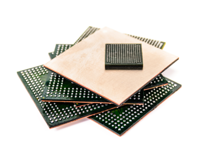
BGA Assembly is an advanced packaging process that achieves electrical connection between integrated circuits (ICs) and printed circuit boards (PCBs) through an array of solder balls arranged at the bottom. Its core feature lies in replacing traditional pins with tin balls, forming high-density, low-resistance interconnection structures via reflow soldering technology. This approach is particularly suited for high-pin-count, high-performance chips such as processors and GPUs.
What Are Pros and Cons of BGA Assembly Service?
Advantages of BGA Assembly Service
High density and miniaturization: Ball grid array layout increases pin count per unit area by 30%-50%. For equivalent capacity, its volume is only one-third of TSOP packages, suitable for miniaturization needs of high-pin-count chips like CPUs and GPUs.
Superior electrical performance: Short-path design reduces parasitic inductance/capacitance, cutting signal transmission delay by 40%-60%. Supports high-frequency applications above 100MHz and high-speed communication with 2-3 times improved crosstalk resistance.
Outstanding thermal efficiency: Solder balls increase contact area by 3-5 times. Combined with metal substrates or thermal materials, chip operating temperature decreases by 15-20°C, ideal for high-power scenarios like servers and automotive electronics.
High mechanical reliability: Solder ball structure buffers thermal expansion stress, improving shock resistance by 50%. Suitable for vibration-prone environments like mobile devices and industrial controls, reducing failure rates by 30%.
Optimized production efficiency: Reflow soldering self-alignment reduces placement errors, improving yield by 10%-15%. Automated equipment supports mass production, cutting costs by 20%-30%
Disadvantages of BGA Assembly Service
Complex inspection and repair: Requires X-ray/industrial CT for internal defect detection (e.g., voids, cracks) with high equipment costs. Rework needs specialized hot air guns or laser reflow devices. BGA becomes non-reusable post-removal, increasing repair costs by 50%-100%.
High costs and technical barriers: Materials (e.g., lead-free solder balls), equipment (high-precision pick-and-place machines), and inspection costs are 30%-50% higher than traditional QFP packaging. Process control requires ±0.05mm placement accuracy.
Environmental sensitivity: Requires strict storage conditions (humidity <10% RH, temperature 20-25°C). Prolonged logistics may cause solder ball oxidation, affecting welding quality.
Coplanarity and warpage risks: Full-array packaging demands coefficient of thermal expansion (CTE) matching between substrate and PCB (difference <5ppm/°C). Otherwise, coplanarity errors or post-soldering warpage may cause voids or shorts.
Competition from alternative technologies: Faces competition from CSP, flip-chip, and other packaging technologies. Requires continuous innovation (e.g., 3D stacked BGA) to maintain market edge, increasing R&D costs by 20%-30%.
Applications of BGA Assembly
Smartphones and tablets: Processors, memory chips, and RF modules.
Laptops: CPUs, GPUs, and mainboard components.
Server systems: Data center CPUs, GPUs, and storage controllers.
High-end graphics cards and workstations: High-speed computing modules.
5G base stations and network equipment: Switch/router integrated circuits.
Automotive systems: ADAS domain controllers, navigation units, and control modules.
Industrial automation: Microprocessors for harsh environment equipment.
Aerospace systems: Satellite/radar microprocessors and image processors.
Medical devices: CT machine data processors and patient monitor chips.
AI and quantum computing: Multi-chip module (MCM) integration platforms.
What Problems Can BGA Assembly Solve?
Enhanced Routing Density: BGA’s bottom grid array design achieves over 1,000 I/O integrations at 0.4mm pitch, increasing pin density by 3-5x compared to traditional QFP packaging. This resolves routing constraints in compact spaces like smartphones and servers. For instance, 0.3mm pitch BGA with laser soldering technology improves ball placement yield to 99.7%, enabling high-density layouts.
Signal Stability Optimization: Differential routing and impedance matching (e.g., PCIe 85Ω/100Ω standards) minimize high-speed signal crosstalk and reflections in 5G base stations and high-end GPUs. Blind/buried via technology shortens signal paths, reducing losses and ensuring stability in high-frequency scenarios.
Thermal Efficiency Improvement: Spherical solder joints expand heat dissipation area, combined with ceramic substrates, thermal via arrays, and heat sinks, to address overheating in high-power chips like GPUs and FPGAs, extending device lifespan.
Process Reliability Enhancement: X-ray inspection and SPC (Statistical Process Control) mitigate hidden defects like voiding and opens in solder joints. Moisture sensitivity classification (per J-STD-020) and baking processes prevent package warpage, while CTE-matched designs reduce solder fatigue in automotive/industrial environments.
Cost-Performance Balance: Standardized packaging supports automated SMT assembly, while HDI (High-Density Interconnect) technology optimizes routing density. This balances performance upgrades with PCB layer count and material cost control, ideal for mass production in consumer electronics. For example, PBGA packaging reduces costs by 30% compared to CBGA while maintaining electrical performance.
Common BGA Package Types
PBGA (Plastic Ball Grid Array)
Substrate: BT resin/glass laminate, solder balls made of 63Sn37Pb eutectic or lead-free solder.
Features: Low cost, good thermal matching (CTE ≈14ppm/°C), compatible with PCB (CTE ≈17ppm/°C), supports self-alignment soldering.
Applications: Consumer electronics chips like CPUs and GPUs, e.g., Intel Pentium II/III/IV processors.
Limitations: Susceptible to moisture (requires moisture-proof packaging), reliability affected by “popcorn effect,” slightly taller than QFP.
CBGA (Ceramic Ball Grid Array)
Substrate: Multilayer ceramic, solder balls use 10Sn90Pb high-temperature solder, requires low-temperature solder for auxiliary connection.
Features: Excellent air tightness (moisture resistance), low thermal conductivity (ceramic substrate CTE ≈7ppm/°C), superior heat dissipation, good electrical insulation.
Applications: High-reliability scenarios like aerospace and military, early Intel Pentium Pro processors.
Limitations: High cost, significant thermal expansion coefficient difference with PCB (causing thermal stress), solder joint fatigue failure risk.
TBGA (Tape Ball Grid Array)
Substrate: PI multilayer wiring substrate, solder balls use high-melting-point solder (e.g., 10Sn90Pb), soldered with low-melting-point solder.
Features: Ultra-thin profile (thickness ≤1mm), better heat dissipation than PBGA, good thermal matching with flexible tape and PCB.
Applications: Mobile devices and high-frequency communication chips, e.g., smartphone processors.
Challenges: Requires X-ray/CT inspection for internal defects, high repair costs, sensitive to humidity (<10% RH).
EBGA (Enhanced Ball Grid Array with Heatsink)
Structure: Integrated metal heatsink or thermal spreader for enhanced heat dissipation.
Applications: High-power chips (e.g., server CPUs), optimized thermal performance via thermal interface materials (TIMs).
BGA Assembly Process Flow
1. Solder Paste Printing Precision Control
Utilize 0.12-0.15mm thick stencils with laser-cut apertures to ensure solder paste volume deviation ≤10% for 0.4mm pitch BGA pads. For sub-0.3mm fine-pitch applications, adopt Type 4 solder paste (particle size 15-25μm) with printing speed 30-50mm/s and squeegee pressure 5-10N to prevent solder defects like insufficient solder, bridging, or collapse. Implement AOI systems for real-time monitoring and automatic adjustment for pads with ≥0.1mm misalignment.
2. 3D SPI Detection & Closed-Loop Feedback
Employ phase-measuring profilometry (PMP) 3D SPI technology for full-field detection of solder paste volume, height, and shape, unaffected by PCB color/reflection. Data feeds back to the printer for dynamic adjustment of squeegee pressure or stencil cleaning. Integrate SPC control to trigger automatic alarms for consecutive critical defects, enabling proactive process optimization.
3. High-Precision Placement & Vision Alignment
Placement machines achieve positioning accuracy ≤±0.03mm and repeatability ≤±0.015mm, with nozzles matched to BGA size/weight. Control placement pressure within 5-20N to avoid PCB warping or pad damage. Post-placement verification via dual-camera vision systems ensures alignment accuracy <1/4 pad diameter; misalignment >0.1mm triggers automatic rework.
4. Reflow Soldering Profile Optimization
Customize four-stage temperature profiles based on solder paste melting points (e.g., 217-227°C for lead-free solder): preheat (150-180°C/60-90s), soak (180-210°C/30-60s), reflow (peak 20-30°C above melting point/30-45s), and cooling (≤4°C/s gradient). Nitrogen atmosphere (O₂ <500ppm) reduces oxidation and void rates. Control furnace temperature uniformity within ±2°C and conveyor speed 50-100cm/min.
5. Multi-Stage Cleaning & Residue Control
Remove flux residues using water-based/semi-aqueous cleaning processes to prevent ionic contamination. For BGA pads, employ specialized cleaners with solder wick to ensure surface flatness. Post-cleaning X-ray inspection verifies solder joint quality, with void rates <25% and no defects like cold joints or bridges.
6. X-ray & AOI Synergistic Inspection
3D X-ray CT scans detect internal defects (voids, cracks, missing solder balls), while 2D X-ray focuses on center and perimeter regions. Post-reflow AOI performs three-point correlation analysis to trace defect origins. Data links to equipment via IPC-CFX protocol for smart factory integration.
7. Electrical Testing & Functional Verification
ICT tests detect solder bridges, opens, and component failures; FT validates circuit continuity and signal integrity. Environmental stress screening (85°C/85%RH/1000h) and ESS accelerate defect detection. Test coverage meets AQL 1.0 standards for reliability assurance.
8. Rework Process & Quality Control
Use hot-air rework stations for BGA removal (preheat ≤120°C, removal temperature matching peak reflow profile). Clean pads and re-place components with secondary vision alignment. Post-rework executes 100% X-ray inspection and functional testing per IPC-7095C standards, with full process data logged for traceability.
Quality Inspection Methods for BGA Assembly
1. Visual Inspection and Surface Defect Screening
Application Scenario: First-article and in-process monitoring on production lines.
Technical Points: Use high-magnification microscopes (≥20X) to inspect solder ball appearance, focusing on bridges, solder balls residue, solder collapse, and oxidation. According to IPC-A-610 standards, the solder wetting angle must be ≤90°, with pad coverage ≥75%.
Limitations: Only detects surface defects; cannot evaluate internal joint integrity.
2. X-ray Inspection Technology (2D/3D)
2D X-ray: Uses planar imaging to detect two-dimensional defects like solder shift, shorts, or insufficient solder volume. Overlapping depth data may cause misjudgment (e.g., stacked layer shadows). Equipment like the YXLON Cougar S series achieves 1μm resolution.
3D X-ray (CT Scanning): Employs tomography for 3D modeling, quantifying void ratios, crack lengths, and interface bonding states. Per IPC 7095, Class 3 products require void diameters ≤30% (or area ≤9%); medical/military sectors demand ≤25%. Space-grade BGA mandates total void area ≤5%.
Principle: Utilizes 50MHz ultrasonic waves to detect delamination, voids, and interface defects via reflection differences. Excels at identifying microvoids ≤50μm.
Case Study: Automotive MCUs undergo C-SAM validation post -40°C~125°C thermal cycling, requiring delamination area ≤10% of joint cross-section. “Popcorn effect” (moisture-induced cracking) is detectable via abnormal attenuation coefficients.
4. Thermal Imaging Testing
Thermal Analysis: Infrared thermal cameras monitor temperature distribution during BGA operation; faulty joints show ≥5°C abnormal rises. Dynamic load testing locates thermal failure points.
5. Electrical Performance Testing
Electrical Test Systems: ICT/Flying Probe: Tests open/short circuits via PCB contact points; 0.4mm-pitch BGA requires spring-loaded probe arrays (±0.02mm accuracy).
Boundary Scan (JTAG): IEEE 1149.1-compliant chip self-testing verifies logic functions and pin connectivity with ≤0.1% false error rates.
High-Frequency Signal Testing: 1GHz+ signals demand insertion loss ≤0.5dB, phase shift ≤5°, using shielded chambers (≥80dB@1GHz) to avoid EMI.
6. Destructive Physical Analysis
Red Dye Penetration Test: Dye penetration visualizes voids/cracks in joint cross-sections. Requires 100°C/4h baking for dye curing, with ≥25mm cutting margins to prevent artificial damage.
Metallographic Cross-Section Analysis: Samples embedded in cold resin undergo grinding/polishing for SEM crack analysis (≤50μm acceptable), paired with EDS for elemental anomaly detection.
7. Environmental Stress and Reliability Verification
Thermal Cycling: -40°C~125°C for 1000 cycles (500 cycles for industrial), 1h per cycle; crack growth ≤50μm. Automotive-grade components require AEC-Q200 certification for 10-year equivalent lifespans.
Ultra-Precision BGA Ball Placement Process with Yield Exceeding 99.8%: Achieves solder ball position accuracy ≤0.02mm through precision mechanical calibration and multi-stage verification, eliminating void soldering/short-circuit risks while reducing client rework costs by over 30%.
Ultra-Fine Pitch PCBA Integration Capability: Supports 01005 component packaging, 2mil line width/spacing, and 40μm laser microvias. Enables integration of over 5,000 BGA solder joints per board, reducing product volume by 40% while increasing functional density by 50%.
7-Day Rapid NPI Verification Service: Four fully automated SMT lines + two dedicated BGA packaging lines enable prototype delivery within 7 days, 40% faster than industry average, accelerating time-to-market for clients.
DFM-Driven Cost Optimization Solution: Optimizes BGA packaging layers through Design for Manufacturability (DFM) analysis, combined with cost-effective material substitution and bulk procurement advantages, reducing total PCBA costs by 15% for enhanced market competitiveness.
End-to-End Transparent Quality Control: MES system enables full barcode traceability from material intake to final shipment, with real-time cloud synchronization of critical process parameters. Clients gain instant access to production progress and quality reports for zero-distance quality monitoring.
Green Manufacturing Compliance System: Uses lead-free solder paste and halogen-free substrates with 100% compliant wastewater/gas emissions. ISO 14001 certified, ensuring seamless compliance with EU RoHS/REACH regulations to avoid trade barriers.
Multi-Scenario Failure Analysis Support: Equipped with X-ray inspection, ultrasonic scanning microscopy, and cross-section analysis tools. Offers 24/7 failure analysis services with root cause reports delivered within 48 hours to minimize production line downtime.
Agile Supply Chain Assurance System: Strategic inventory partnerships with top-tier component manufacturers reduce critical material lead time to 3 days. Multi-site factory coordination ensures stable delivery of large-volume orders while mitigating supply chain risks.
Our BGA Assembly Capabilities
Item
Capabilities
Placer Speed
13,200,000 chips/day
Bare Board Size
0.2″ × 0.2″ – 20″ × 20″ / 22″ × 47.5″
Minimum SMD Component
01005 (0.4mm × 0.2mm)
Minimum BGA Pitch
0.25mm (10mil)
Maximum Components
50mm × 150mm (Board Area)
Assembly Type
SMT / THT / Mixed Assembly
Component Package
Reels / Cut Tape / Tube / Tray / Loose Parts
Lead Time
1 – 5 days (Standard)
How to Get a Quote for BGA Assembly Services?
All documents required to obtain a quote for BAG assembly services:
Submit Design Files: Provide Gerber files, a bill of materials (BOM) (including BGA model/parameters), PCB design drawings, and 3D models (if available). Ensure the file version is the final production version.
Specify BGA technical details: Indicate the BGA pad size, ball diameter, ball pitch (e.g., 0.25mm), package type (e.g., PGA/LGA), and solder requirements (e.g., lead-free/lead-containing).
Confirm production capacity and delivery time: Indicate annual demand, batch order quantity, and target lead time (e.g., 7 days/15 days/30 days). Indicate whether expedited service is required.
Specify testing standards: Indicate whether X-ray inspection, AOI optical inspection, flying probe testing, or functional testing is required, and whether third-party certification (e.g., AEC-Q100) is required.
Indicate material sources: Specify the sourcing method (customer-furnished/contract manufacturing) for BGA chips and other key components, as well as brand preference (e.g., Intel/AMD/Murata).
Fill out the Quote Request Form: Submit the Quote Request Form containing the above information via our official website or designated email address, along with contact information and decision-maker information for follow-up.
Welcome to contact us if you have any request for BGA assembly services: sales@bestpcbs.com.
How to design a mouse PCB? Let’s discover definition, parts, function, types, design guide, production process for mouse PCB.
Are you worried about these questions?
How to cost-effectively mitigate high-frequency signal crosstalk causing cursor jitter?
With urgent projects, how to achieve 72-hour prototyping from design to validation?
How to ensure batch-to-batch performance consistency amid quality fluctuations?
As a mouse PCB manufacturer, EBest Circuit (Best Technology) can provide you service and solutions:
19-Year Process Database Empowerment – Leverage intelligent defect analysis to deliver impedance matching + ground plane segmentation solutions, cutting high-frequency interference costs by 20%!
24-Hour Rapid Prototyping + Free DFM Review – Pre-identify pad spacing/trace width risks to halve prototype cycles, seizing market opportunities ahead of competitors!
Triple Quality Control System – Full coverage of AOI/X-ray/functional testing integrated with ISO 19001 process controls, achieving <3% batch performance variation for reliable mass production!
Welcome to contact us if you have any request for mouse PCB: sales@bestpcbs.com.
What Is a Mouse PCB?
Themouse PCB is a printed circuit board that carries the core electronic components and serves as the hardware hub of the mouse. It integrates components such as a microcontroller, optical sensor, micro switch, and scroll wheel encoder to convert physical operations (movement/click/scrolling) into digital signals, which are then processed and transmitted to the computer via a wired or wireless interface to achieve cursor control and interactive functions.
What Are Parts of Mouse PCBs?
Components of Mouse Printed Circuit Board:
Main Control MCU (Microcontroller): Processes sensor data, executes firmware instructions, manages communication protocols (e.g., USB/HID), and controls peripheral devices.
Optical Sensor: Core positioning component (e.g., PAW series from PixArt), captures surface textures via CMOS imaging, calculates displacement trajectories, and outputs coordinate data.
Micro Switch: Mechanical contact electronic switch (typical model: Omron D2FC-F-7N), converts physical clicks into electrical signals to trigger key responses.
Encoder (Scroll Wheel Module): Mechanical or optical rotary sensor that converts physical scroll wheel rotations into digital pulse signals (e.g., TTC Gold Wheel Encoder).
Wireless Module (Exclusive to Wireless Mice): Integrates 2.4GHz RF chips (e.g., Nordic nRF52 series) or Bluetooth modules for low-latency data transmission and communication with receivers.
Power Management Unit: Lithium battery charging ICs (e.g., TI BQ series) and voltage regulation circuits, providing required voltages for components while optimizing wireless mouse battery life.
Passive Components: Resistor, capacitor, and inductor arrays for signal conditioning, power decoupling, and high-frequency circuit impedance matching (e.g., MLCC capacitors for noise filtering).
LED Driver Circuit: RGB lighting control chips (often integrated into the MCU), driving multi-zone programmable LEDs for dynamic lighting effects.
What Are Function of PCB Mouse?
Below are Functions of PCB Mouse:
High integration and compact layout: Unify all components (MCU, sensors, switches, encoders, LEDs, connectors, passives, wireless modules) on a single platform with stable electrical connections, enabling miniaturized and lightweight design.
Precise signal collaborative processing: Synchronously capture movement signals from optical sensors/roller encoders, click signals from micro-switches, and scroll signals from wheel encoders. Process via MCU for vector calculation, action recognition, DPI switching, and lighting control, then output processed data through wired/wireless channels.
Efficient power management: Distribute power from USB/battery to all components via voltage regulation and filtering circuits, ensuring stable operation and extending battery life while protecting sensitive elements.
Firmware extensibility: Store firmware in built-in/external SPI Flash for dynamic function updates (DPI expansion, light effects, protocol optimization), enhancing maintainability and long-term value.
Multi-mode connectivity: Support USB Type-C/Type-A physical interfaces and wireless antenna interfaces (Bluetooth/2.4GHz), ensuring compatibility with both wired high-speed transmission and stable wireless communication.
Customizable lighting control: Integrate LED driver circuits (MCU-embedded or standalone) and RGB LED pads for user-defined effects (breathing, gradients, game sync), balancing aesthetics with energy efficiency.
Modular expandability: Standardized solder pads and interfaces allow modular replacement/upgrades of sensors and wireless modules, extending product lifecycle and meeting personalized performance/function needs.
What Are Types of Mouse PCB Board?
By High-Density Technology Trends
Multi-layer Rigid-Flex PCB: Adopts 4-layer or higher stacked structures, combining rigid support with flexible connections. Suitable for modular designs (e.g., Razer Viper Ultimate’s “main board + secondary board + display” structure), enabling high-density routing and signal isolation. Meets demands of premium gaming mice for multi-button, RGB lighting, and macro programming.
HDI (High Density Interconnector) Board: Achieves high integration via microvias, blind/buried vias. Applied in compact devices (e.g., Logitech G Pro X Superlight), supporting native 5000-20000 DPI optical sensors (e.g., PixArt PAW series) and high-speed protocols like USB 3.0.
RF PCB: Uses low-loss dielectrics like PTFE or Rogers materials, ideal for wireless mouse RF modules (e.g., 2.4GHz antennas) to ensure signal integrity and noise immunity.
By Heat Dissipation and Lightweight Requirements
Aluminum/Metal Core PCB: High thermal conductivity (1-3W/m·K), used in high-power wireless mice (e.g., Razer Basilisk Ultimate) to extend battery life and enhance structural strength.
Ceramic Substrates: Ultra-high thermal conductivity (Al₂O₃: 24W/m·K), applied in high-precision optical sensor modules to maintain stability during high-speed computation.
By Application Scenarios and Functional Expansion
Office Mouse PCB: Uses single/double-layer FR-4 substrate, integrating low-power sensors (e.g., 5000 DPI optical engines) and basic buttons. Supports multi-surface recognition (glass, wood desks) with emphasis on portability and cost efficiency.
Gaming Mouse PCB: Adopts multi-layer design with high-DPI sensors (e.g., PMW3389, 16000 DPI), programmable buttons, RGB lighting, and macro programming (e.g., MSI DS102 RGB’s 18 RGB LEDs and light guide strip for dynamic effects).
Define parameters: wired/wireless mode, DPI range (e.g., 100-26,000 DPI), key count (left/right/side buttons, DPI toggle), RGB lighting support, battery life (if wireless), and connectivity standards (USB 2.0/3.0, Bluetooth 5.x/2.4GHz).
Specify mechanical constraints: PCB dimensions (based on mouse shell), mount points, key switch footprints, sensor window alignment (for optical sensors), and connector placement (USB-C/Type-A).
2. Component Selection & Bill of Materials (BOM)
MCU Selection: Optimize for ARM Cortex-M4/M7 with hardware accelerators (e.g., NXP LPC55S69 or STM32F4 for DSP instructions). Prioritize GPIO density (≥30 pins), PWM channels (for LED dimming), and integrated peripherals (USB FS/HS, SPI, I²C, ADC for battery monitoring).
Sensors: Optical sensors like PixArt PMW3395 (26,000 DPI, 50g acceleration) or mechanical encoders (e.g., Alps EC11 for scroll wheel). Include gyroscopes/accelerometers for motion tracking in advanced designs.
Power Management: Use low-dropout regulators (LDOs) like TPS7A4500 for 3.3V rails, and buck converters (e.g., TPS62840) for efficient 1.8V/1.2V supplies. Include battery fuel gauges (MAX17048) and protection ICs (DW01A for over-current/short-circuit).
Connectivity & Wireless: USB-C controllers (FUSB302) with CC logic, wireless modules (Nordic nRF5340 with 2.4GHz/BLE 5.3), and antenna matching networks (π-network for 50Ω impedance).
3. Schematic Design & Circuit Partitioning
Power Rail Design: Implement a 3-stage power tree: input from USB/battery → buck converter → LDOs for noise-sensitive rails. Add decoupling caps (10µF electrolyytic + 100nF ceramic) within 5mm of power pins.
Signal Paths: Use star topology for digital traces to minimize crosstalk. Separate analog (sensor) and digital (MCU) ground planes with a single-point connection. Implement Schmitt triggers for switch inputs to debounce signals.
Firmware Interface: Design SPI buses (10MHz) for sensor communication, I²C for auxiliary sensors, and USB HID for configuration. Include a bootloader (e.g., STM32CubeProgrammer) for OTA updates.
Protection Circuits: Add TVS diodes (SMBJ5.0A) on USB lines, polyfuses for over-current, and ESD suppression (ESD7464) on button pads.
4. PCB Layout & Signal Integrity
Layer Stackup: Use a 6-layer stack (signal-ground-power-signal-ground-signal). Route USB differential pairs (90Ω impedance) on inner layers with adjacent ground planes. Place sensitive analog traces (sensor data) on top layer with guard rings.
Component Placement: Cluster the MCU centrally, sensors adjacent to their mechanical windows, and power components near inlets. Orient bypass caps vertically to minimize loop area.
Signal Integrity: Terminate USB lines with 33Ω series resistors. Use ground stitching vias (0.3mm grid) to connect ground planes. For wireless modules, route antenna traces on microstrip layers with 20mm clearance from digital noise.
Thermal Management: Add thermal vias under voltage regulators and LED drivers. Use copper pours (70µm) for heat dissipation. Ensure airflow paths for natural convection.
EMC/EMI Mitigation: Implement ferrite beads on power lines, shield cans for wireless modules, and chokes for high-speed signals. Validate layout against FCC Part 15B/CE RED standards.
5. Firmware & Software Integration
Firmware Architecture: Use a real-time OS (FreeRTOS) for task scheduling. Implement a state machine for button/sensor handling. Optimize power management with sleep modes (e.g., STM32 Stop Mode with RTC wake-up).
Storage: Use SPI Flash (Winbond W25Q16JV) for firmware and user profiles. Include wear-leveling and error correction (ECC) for data integrity.
Configuration Tools: Develop a GUI (Qt/C#) for DPI tuning, lighting effects, and macro programming. Support USB HID and wireless APIs (nRF5340 SDK).
6. Testing & Validation
Functional Testing: Use a USB protocol analyzer (e.g., Total Phase Beagle) for HID traffic. Validate sensor accuracy with a motion test rig. Measure button response time with an oscilloscope.
Signal Integrity: Perform TDR/TDT measurements for impedance control. Use a vector network analyzer for S-parameters. Validate eye diagrams for USB 3.0 compliance.
Power & Thermal: Measure voltage margins with a multimeter. Use thermal cameras to identify hotspots. Validate battery life with a cycle tester.
EMC/Compliance: Test radiated emissions with a spectrum analyzer. Perform ESD testing (IEC 61000-4-2) and surge testing (IEC 61000-4-5).
Durability & Reliability: Conduct vibration testing (MIL-STD-810G), drop testing (1.5m to concrete), and thermal cycling (-40°C to 85°C).
7. Manufacturing & Assembly
DFM/DFA: Use a 2×2 panel with tooling strips. Include fiducials (0.5mm diameter) for pick-and-place. Optimize pad sizes for solderability (ENIG finish).
Material Selection: FR-4 with Tg 170°C for thermal stability. Use high-CTI substrates for safety compliance.
Assembly Process: Use SMT for 01005/0201 passives and BGA/QFN packages. Manual assembly for switches/connectors. Perform AOI and X-ray inspection.
Quality Control: Implement in-circuit test (ICT) for shorts/opens. Conduct functional testing (FT) for all features. Perform burn-in testing (72 hours at 60°C).
How to Make a Mouse PCB Board?
1. Circuit Design Phase
Schematic Design: Utilize EDA software (e.g., Altium Designer, KiCad) to draft the mouse circuit schematic, defining electrical connections for modules like key matrix, optical sensor, microcontroller, and power management. Annotate component parameters (e.g., resistance, capacitance) and package dimensions (e.g., 0603, SOP-8).
PCB Layout Design: Route the PCB based on the schematic, prioritizing signal integrity (e.g., differential pair length matching, impedance control), electromagnetic compatibility (avoiding high-frequency signal crosstalk), thermal design (heat sink placement), and manufacturability (minimum trace width/spacing ≥0.1mm, via size ≥0.3mm).
Gerber File Generation: Output Gerber files (copper layers, solder mask, silkscreen) and Excellon drilling files for subsequent fabrication.
2. Substrate Material Preparation
Material Selection: FR-4 epoxy glass cloth substrate (thickness 1.6mm±0.1mm) with 35μm copper foil (single/double-sided). Verify flatness, copper adhesion, and dielectric constant (typically 4.2–4.8).
Cutting & Cleaning: Cut bulk substrate into standard sizes (e.g., 100mm×100mm). Ultrasonic clean to remove contaminants, ensuring process adhesion.
3. Imaging (Pattern Transfer)
Dry Film Lamination: Apply photosensitive dry film (≈30μm thickness) to cleaned substrate via hot roll lamination, ensuring no bubbles or wrinkles.
Exposure & Development: Use laser photoplotters to generate artwork from Gerber files. UV exposure (365nm, ≈150mJ/cm²) followed by sodium carbonate development to remove unexposed film, forming etch-resistant circuit patterns.
4. Etching & Stripping
Etching Process: Spray copper chloride etchant (250–350g/L, 45–55°C) to remove exposed copper, forming precise circuits. Control etching time (2–3 minutes) to prevent over/under-etching.
Stripping Treatment: Remove residual dry film with sodium hydroxide solution (3–5%), rinse, and dry.
Copper Plating: Deposit conductive layer (≥0.5μm) via electroless copper, then electroplate to thicken (≥20μm) for interlayer connectivity. Acid clean to remove oxides.
6. Solder Mask & Surface Finish
Solder Mask Application: Screen-print liquid photoimageable solder mask (20–30μm thickness) to protect non-soldered areas from oxidation and shorts.
Silkscreen Printing: Add component identifiers, polarity marks, etc., via white silkscreen for assembly reference.
Surface Treatment: Apply HASL (hot air solder leveling), ENIG (electroless nickel immersion gold), or OSP (organic solderability preservative) to enhance pad solderability and oxidation resistance.
7. Profiling & Testing
CNC Profiling: Cut PCB outlines via CNC milling to design specifications (edge smoothness, dimensional tolerance ±0.1mm).
Electrical Testing: Use flying probe or fixture testing to verify continuity, shorts, and impedance.
Functional Verification: Assemble critical components (e.g., microcontroller, buttons) for real-world testing of cursor movement, button response, etc.
8. Packaging & Quality Inspection
Final Inspection: Visual check for defects (solder mask, silkscreen, edges).
ESD-Safe Packaging: Use antistatic bags to prevent electrostatic damage during transit. Label with batch number, production date, and quality grade.
How to DIY a Mouse PCB Board?
1. Circuit Design & Component Selection
Use KiCad or Altium Designer to draw circuit schematics, integrating core components including a microcontroller (e.g., STM32 series), optical sensor (e.g., PixArt PAW3360), micro switches, and USB-C interface. Prioritize sensor data line routing to minimize signal delay, and generate Gerber files for PCB manufacturing.
2. PCB Layout & Impedance Control
Position the optical sensor at the geometric center of the board to reduce offset errors. Surround micro switch pads with grounded copper foil to absorb arc interference. High-speed data traces must maintain equal length and achieve 50Ω impedance matching, avoiding right-angle bends.
3. Substrate Selection & Pattern Transfer
Select a 1.6mm-thick FR4 double-sided copper-clad laminate. Transfer circuit patterns via thermal transfer or photoengraving. For photoengraving, cover the board with negative film and expose it under UV light for 60-90 seconds to harden traces; unexposed areas are removed using developer solution.
4. Precision Etching & Copper Treatment
Etch exposed copper with ammonium persulfate solution (1:8 concentration) at 50°C, agitating continuously to accelerate the reaction. After etching, neutralize with sodium carbonate solution, polish the surface, and apply rosin-alcohol solution for oxidation protection.
5. Drilling & Pad Reinforcement
Drill 0.8mm holes at micro switch pin positions using carbon steel bits, then deburr holes with fine sandpaper. Pre-tin pads using a soldering iron at 350°C to prevent oxidation and enhance soldering reliability.
6. Soldering & Functional Testing
Solder components in sequence: STM32 chip (preheat to prevent cold joints), sensor, micro switches, and USB interface. Power on and test key response rates using open-source firmware (e.g., QMK). Measure sensor supply voltage fluctuations with a multimeter (target: 3.3V±5%).
7. Structural Adaptation & Case Fabrication
Model a 3D-printed case based on PCB dimensions, with a 15°-20° thumb rest angle for ergonomic design. Add 0.5mm clearance around micro switch mounts to prevent key sticking. Attach Teflon feet to the base for smooth movement.
Why Choose EBest Circuit (Best Technology) as Mouse PCB Manufacturer?
Precise Cost Optimization Solutions: Leveraging 19 years of mouse PCB production data to recommend material substitutions and layout optimizations, achieving 15%-30% BOM cost reduction. This directly enhances project profitability and supports budget-sensitive product development.
Rapid Prototyping Capability: 24-hour rapid prototyping for urgent orders, paired with free DFM analysis to pre-identify 30+ manufacturing risks. This reduces prototype validation time to one-third of traditional cycles, accelerating product launch and market capture.
Ultra-Reliable Delivery Performance: 99.2% on-time delivery rate supported by intelligent production scheduling systems, ensuring stable production timelines and minimizing supply chain disruption risks or additional costs from delays.
End-to-End Quality Control: 100% batch inspection with AOI/X-ray/functional testing triple verification, combined with dual ISO 19001/IATF 16949 certified processes, achieving zero-defect bulk shipments and reducing after-sales repair expenses.
Cross-Industry Compliance Assurance: Medical-grade certifications and RoHS compliance enable seamless adaptation from consumer electronics to medical devices, meeting global market access requirements and enhancing product versatility and competitiveness.
Process Expertise from Accumulated Experience: 19 years of vertically integrated manufacturing experience with a database of 2,000+ mouse PCB cases provides proven process parameters and risk forecasting, shortening new project ramp-up time and lowering learning costs.
Customizable Surface Finish Options: Offering HASL/ENIG/OSP and other surface treatment choices to precisely match welding requirements and cost targets, balancing performance with optimal cost efficiency.
Welcome to contact us if you have any request for mouse PCB: sales@bestpcbs.com.
From charging phones to transferring data between devices, USB (Universal Serial Bus) has become one of the most familiar interfaces in electronics everywhere. Universal Serial Bus (USB) is everywhere. But while everyone uses USB daily, few people know how it actually works or how each pin functions inside the connector.
Understanding USB pinout is essential for engineers, PCB designers, and anyone who deals with cable repair or prototyping. Whether you’re working with USB-A, USB-B, or the modern USB-C, knowing each pin’s purpose helps you connect devices safely and efficiently. This guide explains every detail of USB pinouts — including female and male connectors, wire color codes, data transfer principles, and what happens when connections go wrong.
What Is the Pinout for USB?
The USB pinout defines the electrical layout and functionality of the connector’s pins. Each pin has a specific role, such as carrying power, transferring data, or grounding the circuit.
Different types of USB connectors — USB Type-A, USB Type-B, Micro-USB, and USB-C — share similar core principles but have different numbers of pins.
Here’s a simple overview of common USB versions:
USB 1.1 / 2.0: 4 pins (Power, Ground, and two data lines)
USB 3.0 / 3.1: 9 pins (adds extra SuperSpeed data pairs)
USB-C: 24 pins (supports data, power delivery, and video output)
In short, the pinout structure defines how the USB communicates and delivers power between devices.
USB Pinout Diagram
The usb pinout male connector (the plug) is typically what you insert into a device or computer port, while the usb pinout female connector (the receptacle) is what’s mounted on the board or device side.
USB 2.0 Type-A (Male Plug)
Pin
Name
Wire Color
Description
1
VBUS
Red
+5V Power
2
D–
White
Data –
3
D+
Green
Data +
4
GND
Black
Ground
This is the standard configuration used in most USB pinout male connectors. The female connector (socket) has the same pins but in reverse order, facing inward.
USB 3.0/3.1 Type-A (Male Plug)
Pin
Name
Wire Color
Description
1
VBUS
Red
+5V Power
2
D–
White
Data –
3
D+
Green
Data +
4
GND
Black
Ground
5
StdA_SSRX–
Blue
SuperSpeed Receive –
6
StdA_SSRX+
Yellow
SuperSpeed Receive +
7
GND_DRAIN
Black
Ground
8
StdA_SSTX–
Purple
SuperSpeed Transmit –
9
StdA_SSTX+
Orange
SuperSpeed Transmit +
The extra pins in USB 3.0 and newer allow for faster data rates and improved power management.
USB-C Pinout
The USB-C pinout is the most advanced. It’s symmetrical, meaning you can plug it in either way.
Pin
Name
Description
A1, B1
GND
Ground
A4, B4
VBUS
+5V Power
A5, B5
CC
Configuration Channel
A6, B6
D+
USB 2.0 Data +
A7, B7
D–
USB 2.0 Data –
A8, B8
SBU1/SBU2
Sideband Use
A9, B9
VBUS
+5V Power
A12, B12
GND
Ground
A2–A3, B10–B11
TX/RX
High-Speed Data Lanes
USB-C connectors can handle much higher power, up to 100W, and transfer data at speeds exceeding 20 Gbps.
USB Pinout Color Code
The usb pinout color code helps you identify wires easily when stripping or repairing cables. The colors are mostly standardized:
Color
Signal
Description
Red
VBUS
+5V Power
White
D–
Data –
Green
D+
Data +
Black
GND
Ground
Blue/Yellow
SuperSpeed RX/TX (USB 3.x)
High-speed data lanes
Always double-check with a multimeter before soldering or reconnecting wires. While most cables follow this color code, some low-cost ones might differ slightly.
How to Identify USB Pins?
Identifying pins is easier than it looks. Start by checking the USB symbol on the connector to find its orientation. Then, look inside — you’ll see four or more contact pads.
Pin 1 (VBUS) is usually on the left if the port’s wider side faces up.
Pin 4 (GND) sits on the far right.
For a USB pinout male plug:
Pin 1 (VBUS) is on the right when the flat side faces down.
Pin 4 (GND) is on the left.
Using a simple continuity test can also help confirm which pin connects to which wire. It’s especially useful when building custom USB cables or integrating USB interfaces on PCB designs.
Which USB Pin Is Power and Ground?
Power delivery is one of USB’s fundamental functions. The power (VBUS) and ground (GND) pins form the electrical foundation for charging and powering devices.
Pin 1 (Red): +5V DC (VBUS) — supplies power to the connected device.
Pin 4 (Black): Ground (GND) — provides the return path for current.
In older USB versions (1.1 and 2.0), this voltage is fixed at 5V, typically providing up to 500mA of current.
With USB 3.0 and later, the current increases to 900mA, while USB-C supports adjustable power delivery (PD) up to 20V and 5A (100W) depending on negotiation between devices.
If you ever test a USB cable with a multimeter, the red wire corresponds to the +5V pin, and the black one connects to ground.
USB Data Transfer
USB communication happens over differential pairs, meaning the D+ (green) and D– (white) lines carry complementary signals. This design minimizes interference and enables stable, high-speed data transfer. Here’s how data transfer works:
1. The host (computer or controller) initiates communication.
2. The D+ and D– lines transmit binary data in opposite polarity.
3. The device responds through the same lines, completing two-way communication.
USB 2.0 supports up to 480 Mbps, while USB 3.0/3.1 adds new data pairs (SuperSpeed lines) to reach 5 Gbps and 10 Gbps, respectively. USB-C goes even further — supporting USB 4.0 and Thunderbolt modes with speeds over 40 Gbps, depending on configuration.
What Do the Red, White, and Green Wires Do in a USB Cable?
Every wire inside a USB cable plays a unique role:
Red (VBUS): Supplies +5V DC power to charge or operate the device.
White (D–): Carries the negative side of the differential data signal.
Green (D+): Carries the positive side of the differential data signal.
Black (GND): Provides the common return path for current.
If one of these connections is interrupted — for example, a broken white or green wire — the USB will still supply power but won’t transfer data properly. This explains why some damaged cables “charge only” but fail to sync data.
Which USB Wires Are Positive and Negative?
In USB wiring:
Positive: Red wire (VBUS) — supplies +5V.
Negative: Black wire (GND) — completes the electrical circuit.
The data pair (white and green) also has positive and negative roles:
D+ (green) carries positive data signals.
D– (white) carries negative data signals.
This differential system is key for stable and interference-free communication. Always double-check wire polarity before soldering or connecting to avoid damage.
What Happens If I Mix Up Positive and Negative Wires?
Mixing up positive and negative USB wires can damage your devices or ports. If you accidentally reverse them, the circuit might short, causing immediate disconnection or, in worst cases, permanent hardware damage.
The USB port may short-circuit, triggering protection or permanently damaging components.
Devices could fail to boot or suffer electrical damage.
PCB traces might burn due to excessive current.
For this reason, always double-check the pinout before soldering or applying power. Using fuses or protection circuits in prototypes is also a wise practice.
What Happens If You Plug a USB 2.0 into a USB 3.1 Port?
The good news — USB standards are backward compatible. Plugging a USB 2.0 cable or device into a USB 3.1 port will still work safely.
However, data speed will be limited to the lowest standard in the connection. For example, if you connect a USB 2.0 flash drive to a USB 3.1 port, the data rate caps at 480 Mbps instead of 10 Gbps.
Compatibility is one of USB’s greatest strengths — you can mix different generations without damaging your devices.
USB-C Pinout Overview
The usb-c pinout is far more advanced than earlier types. With 24 symmetrical pins, USB-C supports reversible plug orientation, fast data transfer, and powerful charging options.
Here’s a simplified overview of the USB-C pin configuration:
Because USB-C is reversible, you can insert it in either direction — the system automatically recognizes the orientation through CC1 and CC2 pins. It also supports Power Delivery (PD), allowing dynamic voltage adjustment from 5V to 20V, making it suitable for charging laptops, monitors, and industrial equipment.
Why Partner with EBest Circuit (Best Technology) for USB-Related PCB Projects?
Comprehensive engineering support for USB-A, USB-B, Micro-USB, and USB-C connectors
High-quality PCB fabrication with strict impedance control for data traces
ISO-certified quality systems, including ISO9001, ISO13485, IATF16949, and AS9100D
Full traceability system to monitor production and ensure full transparency
Prototype to mass production services, covering cable integration, connector soldering, and testing
Factory based price with no minimum quantity order requirements
Whether you need usb-c pinout-based designs for fast-charging products or usb pinout male/female connectors for embedded systems, EBest Circuit (Best Technology) offers professional solutions tailored to your application
FAQs About USB Pinout
1. What is the difference between USB 2.0, 3.0, and USB-C pinouts?
USB 2.0 has 4 pins—power, ground, and two data lines. USB 3.0 adds five extra pins to support faster data rates up to 5 Gbps. USB-C is more advanced, with 24 pins supporting reversible connections, higher current (up to 5A), and protocols like DisplayPort and Thunderbolt.
2. Can I connect USB male and female cables with different pinouts?
Yes, but only if the pin assignments match. For example, connecting a USB 2.0 male to a USB 3.0 female works because USB 3.0 ports are backward compatible. However, improper wiring or mismatched pinouts may cause unstable connections or charging failure.
3. Why are USB wires color-coded?
The color codes make identification simple during repair or assembly. Red is usually +5V (VCC), black is ground (GND), white is data– (D–), and green is data+ (D+). These color standards help avoid short circuits or reversed connections.
4. Can I use USB pins to power other devices?
Yes, but with caution. Standard USB 2.0 provides up to 500mA, while USB 3.0 can supply 900mA. USB-C supports higher power levels up to 100W (20V/5A) under the Power Delivery (PD) standard. Always check the device’s power requirements before using USB pins as a power source.
5. What should I do if my USB cable gets hot or doesn’t charge properly?
Overheating may indicate a short circuit, incorrect wiring, or poor cable quality. Disconnect it immediately and inspect the pinout. Using cables with the correct gauge and verified USB certification ensures both safety and performance.
Taiwan PCB production has been a global powerhouse for decades. For anyone sourcing electronics, the island’s name is almost synonymous with quality and reliability. We will explore the strengths of the Taiwan PCB industry, weigh it against other options, and introduce a compelling alternative that might just be the smarter choice for your next project.
Are you feeling squeezed between demanding higher quality and managing tighter budgets? Let’s look at some common challenges you might recognize:
Sticker Shock: You receive a quote from a reputable Taiwan PCB company, and the Taiwan PCB price is significantly higher than expected, putting your project’s budget at risk.
Slower Prototype Turnaround: While mass production lead times might be competitive, getting a first-run PCB prototype fabrication can take longer than your development schedule allows.
Less Flexibility for Smaller Orders: Large Taiwan PCB factories are optimized for high-volume runs. They might be less enthusiastic about your initial low-volume or prototype requests.
Hidden Logistics Complexities: Managing shipping and import logistics from Taiwan can add unexpected costs and delays that aren’t always clear in the initial quote.
The solution lies in finding a partner that combines top-tier quality with cost-effectiveness and exceptional service. The ideal partner addresses these issues directly:
Cost-Effective Excellence: They offer competitive pricing without sacrificing quality, giving you the performance you need within your budget.
Rapid Prototyping: They prioritize quick-turn PCB prototype fabrication to keep your product development on track and agile.
Scalability for All Order Sizes: They welcome both small-batch prototyping and large-scale production, growing with your business needs.
Simplified Logistics: A strategic location with well-established shipping routes minimizes transit times and simplifies customs clearance.
This is exactly the kind of partnership we’ve built at BEST Technology. We specialize in high-quality, reliable PCB fabrication and assembly, offering a viable and often superior alternative to traditional Taiwan PCB suppliers. Our focus is on providing quick delivery, responsive service, and manufacturing excellence that meets global standards. If you are working on any PCB projects, please contact us at sales@bestpcbs.com to start a conversation.
What Does “Taiwan PCB” Mean in the Global Electronics Supply Chain?
When we talk about ”Taiwan PCB“, it’s like talking about the Michelin stars of circuit board manufacturing – a symbol of precision, reliability, and cutting-edge innovation. But here’s the exciting part: while Taiwan has long set the standard, manufacturers like EBest Circuit (Best Technology) (Shenzhen) are now not just matching but redefining what excellence looks like.
Technological Leadership:
Taiwanese PCB manufacturers have long been recognized as pioneers in HDI boards and IC substrates, often regarded as the “Apple” of the circuit board industry. Today, EBest Circuit (Best Technology) is establishing itself as a leading innovator in PCB manufacturing:
We produce advanced boards equivalent to Taiwan’s top-tier offerings, including 32-layer HDI boards and ceramic substrates.
Leveraging Shenzhen’s manufacturing ecosystem, we achieve approximately 30% cost reduction and significantly accelerate time-to-market.
Our research and development laboratories operate with the same level of innovation and rigor as Taiwan’s premier manufacturers.
Quality Standards:
Taiwan has set the industry benchmark with its 99.9% quality standards. At EBest Circuit (Best Technology), we not only meet these standards but also elevate them:
Fully certified under IATF 16949, the recognized “gold standard” for automotive-quality PCBs.
Utilizing AI-powered inspection systems to detect defects that may be overlooked by traditional visual inspection.
This approach allows our clients to achieve premium-quality performance with optimized cost efficiency.
Supply Chain Advantage:
Taiwanese PCB manufacturers are renowned for their supply chain reliability. EBest Circuit (Best Technology) builds on this foundation while introducing enhanced responsiveness:
Rapid prototyping: Delivering complex boards in 5 days versus the industry standard of 10.
Flexible order management: Adjusting production volumes weekly without penalties.
A combination of proven reliability and operational agility, akin to merging German engineering precision with Silicon Valley speed.
Global brands are increasingly including EBest Circuit (Best Technology) in their supplier networks due to:
For engineers: Access to advanced technical specifications equivalent to Taiwan boards.
For procurement teams: Achieving 20–30% cost savings, enhancing budget efficiency.
For supply chain managers: Flexibility to accommodate fluctuating demand and unexpected market changes.
In a nutshell, while “Taiwan PCB” remains synonymous with world-class quality, Shenzhen PCB now represents a combination of high-quality, faster delivery, and operational efficiency. EBest Circuit (Best Technology) is proud to define the next chapter in global PCB excellence, offering solutions that balance advanced technology, cost-effectiveness, and agile service.
How Big Is the Taiwan PCB Industry and Who Are the Leading Taiwan PCB Manufacturers?
This section examines the Taiwan PCB industry from both quantitative and qualitative perspectives. We will first highlight the industry’s impressive scale and global influence, then introduce the leading manufacturers that drive innovation and form the backbone of this ecosystem, emphasizing their unique capabilities and strategic partnerships.
Dominant Scale:
The Taiwan PCB industry is not only large—it is the undisputed global leader. For over a decade, Taiwan has consistently ranked first worldwide in terms of production value. According to industry reports from organizations such as Prismark, Taiwan accounts for roughly one-third (over 31%) of the global PCB output value.
To put this in context, if the global PCB market was valued at an estimated $82 billion in 2023, Taiwan’s share would represent approximately $25 billion. This concentration of industry capacity has created an unrivalled cluster effect, ensuring robust supply chain stability, high technical expertise, and rapid innovation capabilities.
Top-Tier Leaders:
Taiwan’s PCB industry is anchored by publicly-listed giants, each specializing in key technologies:
Zhen Ding Technology (Tripod): A world leader in high-density interconnect (HDI) boards and flexible printed circuits (FPCs), Tripod plays a pivotal role in the supply chains for smartphones, laptops, and wearable devices. The company is a critical supplier to major brands such as Apple and is renowned for its cutting-edge manufacturing capabilities.
Unimicron Technology: Dominating the high-end IC substrate market, Unimicron supports advanced semiconductor packaging, producing substrates essential for high-performance GPUs and AI chips. Strategic partnerships with technology leaders like Nvidia underscore its importance in global electronics.
TPT (Taiwan PCB Techvest): A significant player across multiple segments, including HDI and automotive PCBs, TPT demonstrates Taiwan’s diverse manufacturing strength, serving both consumer electronics and industrial applications.
Specialized Champions and Strategic Partnerships:
Beyond these industry giants, a number of specialized manufacturers play critical roles within the supply chain. For example, Cowin is recognized for its expertise in niche PCB technologies and often collaborates with clients such as Nvidia for specialized solutions. Though smaller in revenue compared to the top-tier leaders, these companies offer agility, technical depth, and focused innovation, making them essential partners for complex or highly customized PCB requirements.
In summary, Taiwan’s PCB industry is defined by both scale and specialization. Its top-tier giants, such as Zhen Ding Technology (Tripod) and Unimicron, drive high-volume innovation for leading global brands. Meanwhile, specialized players like Cowin provide essential niche capabilities, adding flexibility and depth to the ecosystem. Together, this layered structure makes Taiwan’s PCB industry a robust, innovative, and indispensable force in the global electronics supply chain.
Why Are Global Buyers Comparing Taiwan PCB Prices with Mainland China’s PCB Manufacturers?
In today’s competitive electronics manufacturing landscape, global procurement teams are conducting meticulous cost-benefit analyses between Taiwanese and Mainland Chinese PCB suppliers. This evaluation has evolved from simple price comparison to a sophisticated assessment of total value, considering differences in cost structures, currency fluctuations, and overall supply chain efficiency. Understanding these dynamics is critical for companies aiming to balance quality, speed, and budget.
The Taiwan PCB Price Structure:
Taiwanese PCB manufacturers are known for premium quality, but this comes with higher costs. Labor costs in Taiwan have risen approximately 35% over the past five years, reflecting the competitive technical workforce. The Taiwan Dollar has appreciated by around 15% against the US Dollar since 2020, which increases international export costs. Additionally, global supply chain disruptions have highlighted certain material dependencies that can affect cost stability and lead times.
Mainland China’s Manufacturing Efficiency:
In contrast, PCB manufacturers in Mainland China—especially in hubs like Shenzhen—benefit from massive scale economies, highly integrated supply chains, and advanced automation, with some facilities reaching over 80% automation rates in critical production processes. These advantages translate into lower manufacturing costs, shorter lead times, and high-quality outputs that meet international standards. Shenzhen’s dense ecosystem of suppliers and technical talent further accelerates prototyping and production cycles, offering a compelling alternative for global buyers.
Beyond Unit Price:
Increasingly, procurement teams evaluate PCB sourcing through Total Cost of Ownership (TCO) rather than focusing solely on unit price. Key considerations include:
Quality and Yield Costs: Higher first-pass yields reduce hidden costs from rework or scrap.
Logistics and Timing: Proximity to components and end markets minimizes transit costs and delays.
Supply Chain Resilience: Diversified manufacturing reduces risks from single-point failures.
Technical Support: Close collaboration with engineering teams accelerates product development.
This holistic view highlights why Mainland Chinese suppliers, especially Shenzhen-based manufacturers like EBest Circuit (Best Technology), are increasingly preferred for both prototyping and volume production.
Strategic Sourcing in Practice:
Leading electronics companies now adopt structured frameworks to compare Taiwan and Mainland Chinese PCB suppliers. This includes simultaneous RFQs with identical specifications, facility audits, and sample validation. While Taiwan PCB manufacturers excel in advanced HDI boards, flex PCBs, and IC substrates, many buyers are turning to Shenzhen suppliers for faster lead times, lower TCO, and responsive technical support.
EBest Circuit (Best Technology) exemplifies this new standard. As a Shenzhen-based PCB manufacturer, we offer:
Advanced PCB capabilities equivalent to top-tier Taiwan suppliers (HDI, heavy copper, flex/ridig-flex, ceramic PCBs).
Rapid prototyping and production: First-run boards delivered in 24–48 hours, significantly faster than Taiwan standard lead times.
Cost-efficiency: Achieving 20–30% lower TCO through supply chain optimization and Shenzhen’s manufacturing ecosystem.
By leveraging Shenzhen’s operational advantages without compromising on technology or quality, EBest Circuit (Best Technology) provides global buyers with a practical, cost-effective alternative to traditional Taiwan PCB suppliers.
Taiwan PCB vs. Shenzhen PCB Manufacturing – What’s the Real Difference?
This is the core of the modern sourcing debate. On one side, you have the established quality of Taiwan PCB factory production. On the other, the agility and cost savings of Shenzhen PCB manufacturing. So, what are the real distinctions?
Cost Structure: Generally, Shenzhen offers lower manufacturing costs due to economies of scale, lower labor costs, and a highly competitive local supplier network.
Speed and Flexibility: Shenzhen’s ecosystem is built for speed. The proximity of suppliers, component distributors, and assembly houses allows for incredibly fast PCB prototype fabrication and turnarounds. This is a huge advantage for startups and companies with fast-paced development cycles.
Technological Parity: The gap has narrowed significantly. Top-tier Shenzhen printed circuit board manufacturers now operate state-of-the-art facilities that rival those in Taiwan, especially for standard and advanced PCB types.
The difference, therefore, is less about quality and more about operational efficiency and accessibility for many international customers.
Why More Companies Choose Shenzhen PCB Manufacturers Over Taiwan PCB Suppliers?
A paradigm shift is occurring in global electronics procurement as OEMs increasingly partner with Shenzhen-based manufacturers like EBest Circuit (Best Technology) instead of traditional Taiwanese suppliers. This transition stems from an optimal convergence of economic efficiency, technical capability, and supply chain agility that aligns perfectly with contemporary product development requirements.
Substantial Cost Efficiency Without Quality Compromise
Shenzhen manufacturers achieve 25-40% cost advantages versus Taiwanese counterparts through:
EBest Circuit (Best Technology)’s proprietary “Tiered Cost Optimization” system for multilayer boards (1-32L)
Direct material sourcing partnerships delivering 15-20% substrate cost reductions
Automated production lines reducing overhead by 18% compared to manual processes
EBest Circuit (Best Technology) maintains IATF 16949 and IPC Class 3 certification while achieving <500ppm defect rates, demonstrating that cost savings don’t compromise quality.
48-hour global logistics via Hong Kong/Shenzhen ports
Local supplier network: 90% materials within 15km radius
Technical ecosystem: Immediate access to component markets
Quantified as 28% faster total lead time versus Taiwan-based alternatives.
The Technical Differentiation
While Taiwanese suppliers maintain niche capabilities, EBest Circuit (Best Technology) represents the new benchmark through:
Total Cost Advantage: Documented 37% savings versus comparable Taiwan bids
Technical Agility: One of the top Shenzhen manufacturers with both 20oz heavy copper and 0.15mm ultra-thin capabilities
EBest Circuit (Best Technology) — A Smarter Alternative to Taiwan PCB Suppliers
EBest Circuit (Best Technology) has emerged as a strong alternative to traditional Taiwan-based PCB manufacturers, combining international-quality technical capabilities with the distinct advantages of our Shenzhen-based operations. We offer comprehensive PCB solutions that balance high standards of quality with competitive cost-efficiency, making us an increasingly preferred choice for global customers.
Key Advantages:
Technical Parity with Superior Cost Structure
Matches Taiwan’s advanced PCB capabilities (1-32L boards, HDI, RF, heavy copper up to 30oz)
30-40% cost savings through Shenzhen’s mature supply chain ecosystem
Maintains ±3mil tolerance standards comparable to Taiwan’s premium suppliers
Advanced testing: • 100% impedance control (±5Ω for ≤50Ω designs) • 3D X-ray inspection for μBGA (<0.2mm pitch)
As your strategic manufacturing partner, EBest Circuit (Best Technology) delivers Taiwan-grade PCB technologies with mainland China’s efficiency and cost benefits. Our vertically integrated solutions—from design support to box-build assembly—ensure seamless product realization while optimizing your time-to-market and total cost of ownership.
Case Study: US Client Cuts 30% Costs by Switching to EBest Circuit (Best Technology)
A concrete example shows the real-world impact. A U.S.-based client in the IoT sector came to us with a challenge. They were using a well-regarded Taiwan PCB manufacturer for a complex 8-layer board. While the quality was good, the costs were high, and lead times were stretching their development schedule. They needed a change.
The Situation:
Previous Supplier: A major Taiwan PCB supplier.
Product: Complex 8-layer PCB with impedance control.
Pain Points: High Taiwan PCB price, slow response times, and extended lead times for prototypes.
Our Solution: Our team conducted a thorough Design for Manufacturability (DFM) analysis. We identified a few minor optimizations that could be made to the panel design to improve yield without affecting performance. We then provided a transparent quote that was 30% lower than their existing cost. Most importantly, we guaranteed a much faster turnaround for their PCB prototype fabrication.
To conclude, Taiwan PCB manufacturing remains a formidable force in the global electronics industry. This article has explored its strengths and the reasons why many businesses are now considering alternatives like Shenzhen-based manufacturers. For those seeking a partner that offers uncompromising quality, significant cost savings, and exceptional service, BEST Technology stands ready. We provide a compelling alternative to traditional Taiwan PCB suppliers. Pls feel free to reach out to our team today at sales@bestpcbs.com for a quick, no-obligation quote.
Why choose Polyimide copper laminate for flexible PCB? Let’s discover its definition, benefits, selection guide, spec, difference between adhesive-less and adhesive, common material supplier.
Are you troubled with these questions?
Are you facing reliability issues in flexible circuits due to inadequate bend resistance of polyimide copper laminate?
How to prevent high dielectric loss from compromising signal integrity during high-frequency signal transmission?
How to achieve rapid delivery for small-batch, multi-variety orders while maintaining cost efficiency?
As a flexible PCB manufacturer, EBest Circuit (Best Technology) can provide you solution:
Nano-modified PI substrate with gradient copper foil design achieves 200,000 crack-free cycles at 0.5mm bend radius, extending operational lifespan by 40%.
Low-dielectric (Dk < 3.0) modified PI material combined with 3D microstrip line optimization reduces insertion loss by 20%, ensuring robust signal integrity during high-frequency transmission.
Modular design and intelligent production scheduling enable 2-hour line changeovers, 72-hour global direct delivery, and maintain cost efficiency with only a 20% premium over mass production costs.
Welcome to contact us if you have any request for flexible PCB: sales@bestpcbs.com.
What Is Polyimide Copper Laminate?
Polyimide Copper Laminate is a high-performance electronic substrate material composed of polyimide film (insulating substrate) and conductive copper foil, bonded through specialized processes such as high-temperature lamination or direct copper bonding techniques. Its core value lies in integrating polyimide’s extreme temperature resistance (capable of enduring prolonged exposure to temperatures above 260°C), exceptional flexibility (withstanding repeated bending), and copper foil’s superior electrical conductivity.
This combination makes it a critical foundational material for manufacturing flexible printed circuits (FPC) and high-temperature/high-frequency rigid circuit boards, particularly suited for demanding applications requiring both high-temperature stability and dynamic bending capabilities, such as smartphone foldable screens, aerospace electronics, and automotive engine compartment control units.
Why Choose Polyimide Copper Laminate for Flexible PCB?
Extreme Temperature Resistance: Withstands prolonged exposure above 260°C, ensuring stable operation in high-temperature environments like automotive engine compartments and aerospace electronics. Reduces equipment failure risks, maintenance costs, and downtime losses.
Dynamic Flexibility Adaptation: Supports repeated bending, ideal for scenarios requiring frequent dynamic deformation (e.g., foldable smartphone screens, wearables). Enhances design freedom and space utilization while preventing circuit cracking from mechanical fatigue.
Efficient Signal Transmission: Copper foil’s superior conductivity enables low-impedance, high-frequency signal transmission. Minimizes signal loss in 5G and high-frequency devices, improving response speed, accuracy, and end-product performance.
Lightweight & Thin Design: Polyimide substrate’s lightweight, thin profile supports weight reduction and thinning of circuit boards. Suitable for portable devices (e.g., foldable smartphones) and spacecraft components, driving compact, portable product innovation.
Chemical Stability: Corrosion-resistant and chemically inert properties maintain stability in harsh environments (e.g., high humidity, chemical pollution). Extends device lifespan by reducing environmental aging and long-term usage costs.
Thermal Management Optimization: Good thermal conductivity aids heat dissipation, preventing performance degradation or component damage from localized overheating. Ensures stable operation in high-power computing and electronic devices.
Process Compatibility: Highly compatible with existing flexible PCB manufacturing processes (e.g., high-temperature lamination, microvia processing). Reduces conversion barriers, shortens development cycles, and lowers technical transition risks/upfront investment.
Long-Term Cost Efficiency: While initial material costs may be higher, its durability, fatigue resistance, and long lifespan reduce maintenance/replacement frequency. Saves hidden lifecycle costs and improves overall ROI.
How to Choose Polyimide Copper Laminate for Flexible PCB?
1. Precise Adaptation of Basic Parameters to Application Scenarios
Thickness Stratification Design: Base material thickness must dynamically match bending radius, conventional flexible PCBs use 12.5-50μm PI; high-frequency applications (e.g., 5G antenna modules) prioritize 8-12μm ultra-thin PI to minimize signal loss; high-power scenarios (e.g., automotive power control modules) require 25-50μm thick PI for enhanced thermal stability.
Copper Foil Type Selection: Electro-Deposited (ED) copper offers cost advantages for static or low-frequency bending scenarios; Rolled Annealed (RA) copper, with its dense grain structure, achieves >100,000 dynamic bending cycles, ideal for foldable smartphones and wearables.
Mandatory Flame Retardancy Standards: Medical implants and automotive engine compartment electronics must meet UL94 V-0 flame retardancy to ensure safety redundancy in extreme environments.
2. Quantitative Validation of Thermal Performance Metrics
Glass Transition Temperature (Tg) Grading: Conventional PI substrates have Tg ≥200°C for consumer electronics; industrial control modules require Tg >250°C specialty PI (e.g., DuPont Kapton® KJ series); aerospace applications near engines demand custom Tg >350°C materials.
Coefficient of Thermal Expansion (CTE) Matching: X/Y-axis CTE must be controlled within 12-18ppm/°C to form a gradient match with copper foil (17ppm/°C), preventing interlayer delamination from thermal stress concentration.
Low-Loss Dielectric Constant (Dk) Selection: High-frequency circuits (>1GHz) require Dk <3.0 PI-Cu materials like DuPont Pyralux AP or Ube Upilex-SA to reduce signal delay and loss.
4. Dynamic Durability Testing of Mechanical Properties
Standardized Peel Strength Verification: 1oz copper foil must achieve ≥0.8N/mm peel strength (IPC-6013 standard), validated via 90° peel testing for interfacial adhesion.
Quantitative Bend Life Testing: Dynamic bending applications require ≥50,000 MIT fold cycles with a fold radius ≥3× material thickness; high-reliability scenarios (e.g., aerospace) demand >100,000 cycles.
5. Chemical Compatibility and Environmental Adaptability
Full-Process Chemical Resistance Validation: Compatibility testing covers electroplating (copper/nickel sulfate), solder mask (epoxy/polyurethane), and other process chemicals to prevent material swelling or degradation.
Moisture Absorption Control: Prefer hydrophobic modified PI (e.g., Mitsubishi Gas Neopulim®) with <0.8% moisture absorption to mitigate electrical performance drift in high-humidity environments.
6. Supplier Qualification and Batch Stability
Full-Chain Certification Traceability: Suppliers must provide UL certification, ISO9001/14001 system certificates, and batch variation reports (±3% standard) for key parameters (Tg, CTE, peel strength) over six months.
Supply Chain Risk Management: Prioritize suppliers with global delivery capabilities (e.g., DuPont, SABIC) and assess geopolitical risks impacting supply continuity.
7. Cost Optimization and Customization Strategies
Stratified Cost Optimization: Non-critical layers (e.g., ground planes) may use low-Tg PI to reduce costs; high-frequency signal layers employ specialty low-loss PI for performance-cost balance.
Bulk Customization Services: For orders >500m², negotiate custom solutions for copper foil thickness (e.g., 9μm/18μm), adhesive systems (acrylic/epoxy), and process requirements (e.g., laser microvia precision ±2μm).
0.002–0.025 @1 GHz–10 GHz (≤0.005 for high-frequency applications)
Glass Transition Temperature (Tg)
>250 °C (Flexible), >260 °C (Rigid)
Thermal Decomposition Temperature (Td)
>400 °C
Z-axis CTE
20–70 ppm/°C (<Tg)
Peel Strength
≥1.0 N/mm (Flexible), ≥1.5 N/mm (Rigid)
Water Absorption Rate
<0.5% (Flexible), <0.3% (Rigid)
Flame Retardancy Rating
UL94 V-0
Dimensional Stability
≤0.1% (MD/TD Directions)
Difference between Adhesive-less vs. Adhesive Polyimide Copper Laminate
Structural Composition
Adhesive-less Polyimide Copper Laminate(2L-FCCL): Composed of two layers, polyimide (PI) film directly bonded to copper foil without additional adhesive layers.
Adhesive Polyimide Copper Laminate (3L-FCCL): Consists of three layers, PI film, organic adhesive (e.g., acrylic or epoxy resin), and copper foil.
Thermal Performance & Reliability
Adhesive-less Polyimide Copper Laminate: Superior high-temperature resistance, thermal dimensional stability, and long-term reliability due to the absence of thermally inferior adhesive layers. Withstands harsh conditions like soldering above 300°C.
Adhesive Polyimide Copper Laminate: Organic adhesive layers exhibit poorer thermal stability, softening or degrading above 150°C, leading to reduced peel strength and compromised reliability.
Thickness & Weight & Flexibility
Adhesive-less Polyimide Copper Laminate: Thinner, lighter, and more flexible, ideal for dynamic bending applications and high-density wiring.
Adhesive Polyimide Copper Laminate: Thicker and heavier due to adhesive layers, with reduced flexibility.
Electrical Performance
Adhesive-less Polyimide Copper Laminate: Stable dielectric properties, lower dielectric loss, and better impedance control, suitable for high-frequency/high-speed applications.
Adhesive Polyimide Copper Laminate: Adhesive layers may introduce additional dielectric loss and moisture absorption, potentially affecting electrical stability.
Peel Strength & Bonding Process
Adhesive-less Polyimide Copper Laminate: Direct chemical bonding (e.g., coating, lamination, or sputtering) between copper and PI ensures high initial peel strength and stability at elevated temperatures. Requires high-purity PI films with excellent bonding properties.
Adhesive Polyimide Copper Laminate: Relies on physical adhesion from adhesives, offering good peel strength at room temperature but significant degradation at high temperatures. Manufacturing processes are simpler and more mature.
Cost & Applications
Adhesive-less Polyimide Copper Laminate: Higher cost due to complex manufacturing and stringent technical requirements. Used in high-end, high-reliability fields such as aerospace, military electronics, premium consumer electronics (foldable smartphones), automotive electronics, rigid-flex PCBs, and HDI boards.
Adhesive Polyimide Copper Laminate: Lower cost and mature processes, widely applied in cost-sensitive, moderate-environment flexible circuits.
Dimensional Stability
Adhesive-less Polyimide Copper Laminate: Lower coefficient of thermal expansion (CTE), minimizing dimensional changes during thermal cycling for high-precision circuits.
Adhesive Polyimide Copper Laminate: Adhesive layers are prone to dimensional changes under heat, resulting in poorer overall stability.
Common Polyimide Copper Clad Laminate Supplier
DuPont (USA)
Products: Kapton® series polyimide film-based copper-clad laminates.
Advantages:
Extreme temperature adaptability (-269°C to +400°C) for aerospace/automotive electronics; dielectic strength 3000–6000 V/mil, volume resistivity >10¹⁵ Ω·cm.
Global supply chain with 40+ years’ experience, rapid delivery for large orders, and global technical support.
Rogers Corporation (USA)
Products: High-frequency/high-speed CCLs (RO3000, RO4000 series) and hybrid polyimide materials.
Advantages:
Leading high-frequency performance (Dk 2.2–6.15, Df 0.001–0.004) for 5G/millimeter-wave radar; 50%+ global market share in RF/microwave, 60+ years’ expertise.
Customizable hybrid designs (e.g., ceramic-filled PTFE) for multi-layer/hybrid circuits; UL-certified.
Kaneka (Japan)
Products: Apical® polyimide film and flexible CCL (FCCL).
Advantages:
Ultra-thin film (7.5μm and below) for high-density flexible circuits (foldable phones/wearables); 80%+ global TPI market share for adhesive-free 2L FCCL.
Stable Asian supply chain (Japan-based production) with short lead times.
Panasonic (Japan)
Products: High-speed CCLs (Megtron series) and polyimide-ceramic composites.
Advantages:
Low loss (Df < 0.005) and stable Dk for servers/high-speed communication; advanced Dk control in high-temperature lamination.
Halogen-free/RoHS compliance for EU/North American markets.
Cost-effective high-frequency options (Dk 3.0, Df 0.0017) vs. Rogers; compatible with FR-4 processes for hybrid designs.
Global production network (USA/Europe/Asia) for regional supply chain optimization.
Where Can I Buy a Reliable Polyimide Copper Laminate Board?
Professional B2B Procurement Platforms
Alibaba International Station: Supports small-batch procurement (e.g., minimum order quantity of 10 square meters), provides integrated logistics and payment services, and allows screening of suppliers from Guangdong, Jiangsu, and other regions.
Global Sources: Focuses on the electronics industry, supports free registration, allows listing of 100 products, and links with Hong Kong international exhibitions, suitable for professional buyers.
Made-in-China.com: Covers over 3,500 product categories, supports 11 languages, accounts for 84% of overseas buyers, with an annual fee of CNY 31,100 for Audited Suppliers, ideal for SMEs.
International Certifications & Standard References
UL Certifications: UL 796 (printed circuit substrates) and UL 94 (flame retardancy, e.g., V-0 rating) ensure material safety and electrical performance.
ISO Systems: ISO 9001 (quality management), RoHS (environmental compliance), and REACH (chemical safety) guarantee regulatory compliance in production.
Chinese National Standard GB/T 16315-2017: Specifies electrical, thermal (glass transition temperature ≥200°C), and mechanical (peel strength ≥60N) performance for copper-clad polyimide glass fabric laminates.
Logistics & Customs Clearance Services
Logistics Options: Select air freight (fast), sea freight (cost-effective), or international couriers (e.g., DHL, FedEx) based on volume, weight, and delivery time. High-value shipments are recommended for air/express with transport insurance.
Customs Documents: Prepare invoices, packing lists, certificates of origin, UL/ISO certification files, and comply with destination country requirements (e.g., Russia/Ukraine’s lenient air clearance, Africa’s “gray customs” risks).
Overseas Warehousing: Moscow (Russia) and Almaty (Kazakhstan) overseas warehouses support local clearance and dropshipping, suitable for e-commerce and bulk orders.
Payment & After-Sales Guarantees
Payment Methods: Telegraphic Transfer (TT), Letter of Credit (LC), third-party platforms (PayPal, Western Union), and Open Account (OA) terms, chosen based on transaction value, country risk, and supplier requirements.
After-Sales Support: Confirm suppliers offer technical support, return/replacement policies, and long-term supply capabilities. Contracts must specify quality standards, delivery timelines, liability clauses, and dispute resolution (e.g., international arbitration).
Industry Resources & Expansion Channels
Exhibitions & Associations: Participate in China Electronics Fair (CEF) and International Electronics Circuit Exhibition (CPCA) for direct supplier engagement and technology updates.
Technical Forums: Utilize platforms like Zhihu and Guide Chemical Network Community for peer insights and supplier reviews.
Customs & Logistics Advisory: Monitor destination country regulations (e.g., EU CE certification, U.S. FCC compliance) and logistics timelines to plan shipments proactively.
Welcome to contact us if you have any other issues about Polyimide copper laminate: sales@bestpcbs.com.
PCB manufacturer USA represents a vital link in the American electronics supply chain. Choosing the right partner for your printed circuit boards is one of the most critical decisions you will make. This article provides a clear look at the US PCB manufacturing scene. We will explore its competitiveness, the challenges buyers face, and why a growing number of companies are finding success with a hybrid approach that includes overseas expertise.
Have you ever felt overwhelmed while searching for a reliable printed circuit board manufacturers USA? Many engineers and procurement specialists encounter similar roadblocks.
The High-Cost Hurdle: The initial quotes from some domestic shops can be staggering. This often puts a strain on budgets, especially for prototypes or small-batch production.
The “Black Box” of Production: After you place an order, communication can drop off. You are left wondering about the status of your boards. A lack of clear, proactive updates creates unnecessary stress.
Limited Specialized Capabilities: You might have a complex design requiring advanced materials, like flex or rigid-flex boards. Not every PCB factory USA has the equipment or expertise to handle these specialized projects effectively.
Inflexible Lead Times: Standard lead times of several weeks can derash tight development schedules. The need for a true quick turn PCB service is often more talked about than delivered.
Inconsistent Quality: Perhaps the most worrying issue is receiving boards that don’t meet your specified standards. This leads to costly reworks, delays, and frustration.
Fortunately, these common pain points are not dead ends. They are solvable problems.
Cost Transparency and Value Engineering: A good partner provides detailed, transparent quotes. They will also suggest smart design-for-manufacturability (DFM) tweaks. These small changes can significantly reduce your costs without compromising performance.
Proactive and Open Communication: You should expect a dedicated point of contact. They will provide regular updates throughout the process. This includes real-time production tracking, so you are never left in the dark.
Expertise in Advanced Technologies: Look for a PCB board manufacturer USA with a proven track record in your specific need. Whether it’s flex PCB manufacturer USA capabilities or rigid flex PCB manufacturer in USA services, their expertise should be demonstrated.
Commitment to Speed and Reliability: A true partner understands that time is critical. They offer dependable expedited services, like 24 hour PCB prototyping, that you can actually count on to meet your deadlines.
A Quality-First Guarantee: The best partners have robust quality control systems. They should be willing to share their certifications and quality reports. This ensures that every board you receive is right the first time.
EBest Circuit (Best Technology) is a specialized Chinese PCB company with deep roots in both advanced engineering and efficient manufacturing. Our team is passionate about turning complex designs into reliable, high-performance circuit boards. We combine technical expertise with a commitment to clear communication and fast delivery. Feel free to reach out to us at sales@bestpcbs.com to discuss your project’s unique requirements.
Top PCB Manufacturer USA
The search for a “Top PCB Manufacturer USA” is a critical first step for any electronics project. The US market is not a monolith; it’s a rich ecosystem of specialized providers. Here are three examples of established US-based manufacturers, each with a different focus:
San Francisco Circuits (SFC)
Brief Introduction: Based in Silicon Valley, SFC positions itself as a technology leader, particularly for highly complex, advanced PCBs. They specialize in HDI (High-Density Interconnect), rigid-flex, and boards with demanding specifications for the aerospace, medical, and high-performance computing industries. They emphasize strong engineering support from the design phase onward.
Advanced Circuits (a division of APCT)
Brief Introduction: As one of the largest commercial PCB manufacturers in the country, Advanced Circuits is known for its reliability and extensive service offerings. They are a go-to for quick-turn prototypes and mid-to-high volume production, serving a broad base of customers. Their user-friendly online quoting and ordering platform makes them a popular choice for engineers and procurement teams needing consistent, dependable service.
TTM Technologies
Brief Introduction: TTM is a global giant in PCB manufacturing, with significant operations and advanced technology centers within the United States. They cater to the most demanding end-markets, including aerospace/defense, networking/communications, and medical. Their scale allows them to handle extremely complex, multi-layer boards and full box-build assembly, making them a partner for large-scale, mission-critical applications.
In summary, the “Top PCB Manufacturer USA” title is earned in different ways. There is no single “best” option, only the best option for your specific project’s requirements. The landscape is competitive and robust, offering everything from rapid-turn prototyping shops to massive technology leaders. The key to success is matching your needs for complexity, volume, and speed with a manufacturer whose strengths are a perfect fit, ensuring a successful partnership from prototype to production.
How Many PCB manufacturers in USA?
Getting a single, precise number for PCB manufacturers in the USA is challenging. The market is dynamic, with the count fluctuating due to economic conditions, mergers, and new startups. However, industry analysis consistently points to an estimated 500 to 800 established PCB manufacturing facilities operating nationwide. This section breaks down what this number truly means for a buyer, examining the market’s structure, cost drivers, and core competencies.
1. Market Scale and Competitive Landscape
The US PCB market is not a single, homogenous block. It’s a diverse ecosystem segmented by geography, size, and specialization.
Geographic Clusters: Manufacturing is not evenly distributed. Significant clusters are found in:
California & the West Coast: A hub for serving the aerospace, defense, and Silicon Valley tech industries, often specializing in high-tech, low-to-mid volume production.
Midwest (e.g., Michigan, Illinois): Strongly tied to the automotive and industrial sectors, with expertise in robust, high-reliability boards.
Northeast and South: Home to a mix of large-scale commercial producers and specialized shops serving military and medical applications.
Market Structure: The landscape is fragmented. It is not dominated by a few giants. Instead, it features a handful of large-scale players (like TTM Technologies) alongside a long tail of hundreds of small and medium-sized enterprises (SMEs). This means buyers have a wide range of choices, but finding the perfect fit requires careful research.
2. Cost and Price Considerations
The question of “PCB manufacturing USA cheap” options requires a realistic perspective.
Cost Drivers: Labor rates, regulatory compliance, and energy costs are significantly higher in the US than in Asia. This inherently results in a higher price point. A board fabricated in the US will almost always have a higher unit cost than a directly comparable board made overseas.
The “Cheapest” Myth: While some shops compete aggressively on price, the search for the “cheapest PCB manufacturer USA” can be risky. Extremely low prices may come with compromises in material quality, testing rigor, or customer service. The real value proposition of US manufacturing is rarely the lowest initial cost.
3. Technical Capabilities and Specializations
The key is to look beyond the total number of manufacturers and focus on those with the right expertise for your project.
Advanced Technology Leaders: A select group of US manufacturers are global leaders in producing highly complex boards. They excel in:
HDI (High-Density Interconnect) and ultra-fine line PCBs.
Flex and Rigid-Flex circuits for advanced electronics.
RF/Microwave and High-Speed boards for communications and defense.
Prototype and Quick-Turn Services: This is a major strength of the US market. A large number of shops, from small specialists to large divisions within big companies, offer excellent prototype PCB and quick turn PCB services. This is a primary reason buyers choose domestic production.
4. Production Lead Times and Responsiveness
Speed is a definitive advantage for US-based production.
Domestic Speed: Proximity to customers allows for much faster turnaround times. Many US manufacturers reliably offer quick turn services, including 24 hour PCB prototyping for simple designs. This agility is critical for rapid iteration in product development.
Supply Chain Efficiency: A domestic supply chain avoids potential delays from international shipping, customs, and time-zone communication gaps. This leads to more predictable and often faster overall delivery.
5. The Overseas Manufacturing Alternative
Any evaluation of US manufacturers is incomplete without a comparison to overseas options, particularly in Asia.
The Cost Gap: The cost difference can be substantial, often ranging from 20% to 50% less for equivalent volume production overseas. This is the primary driver for companies to look abroad.
Quality Parity? Many top-tier overseas manufacturers, especially in China, are certified to the same international quality standards (like ISO, IATF 16949) as US shops and can produce boards of equal technical quality.
The Hybrid Decision: The choice often boils down to a trade-off: US manufacturing offers speed, communication ease, and IP security, while overseas manufacturing offers significant cost savings, especially for high volumes. Many companies adopt a hybrid model, using US shops for prototyping and initial production, then shifting volume manufacturing overseas.
In summary, the estimated 500-800 US PCB manufacturers represent a mature and highly segmented market. While the initial cost is higher, the value lies in advanced technical expertise, unparalleled speed for prototyping, and a resilient supply chain. The decision to “buy American” is ultimately a strategic one, balancing budget constraints against the critical needs for speed, specialized capability, and supply chain control.
How Competitive Is the PCB Manufacturing Industry in the USA?
The US market is highly competitive, but in a unique way. It is not typically a competition on price alone. Instead, top rated PCB manufacturer USA competitors differentiate themselves on other critical factors.
How Competitive Is the PCB fabrication USA? The competition is fierce, but it revolves around value, not just cost.
Quality and Reliability: For industries where failure is not an option, US manufacturers emphasize their rigorous quality standards. This is a significant competitive advantage.
Advanced Technological Capability: Many US shops invest heavily in state-of-the-art equipment. They excel at producing highly complex, multi-layer, and HDI boards that are difficult to manufacture.
Speed and Responsiveness: Proximity to customers allows many US manufacturers to offer faster turnaround times for prototypes and quick-turn production. This is a key selling point.
Supply Chain Security: Having a domestic supplier reduces reliance on international logistics. This minimizes risk from geopolitical issues or global disruptions, which is a major concern for many businesses.
IP Protection: Manufacturing within the US offers stronger legal protections for intellectual property. This is crucial for companies working on cutting-edge, proprietary technologies.
In short, the PCB fabrication USA market competes by offering superior service, technological leadership, and reduced risk. This is the value proposition that resonates with their target customers.
What Challenges Do PCB Buyers Face When Choosing Printed Circuit Board Manufacturers USA?
Even with many options available, buyers can still run into difficulties. The process of selecting a PCB maker USA involves navigating several common challenges.
Navigating the Cost-Quality Balance: Finding the cheapest PCB manufacturer USA is easy. But finding one that also delivers high quality is the real challenge. Buyers must carefully evaluate what is included in a quote to avoid hidden costs or quality compromises.
Verifying True Capabilities: A company’s website might claim they can build anything. The reality can be different. It can be hard to verify if a PCB factory USA has real experience with your specific board type, such as high-frequency or heavy copper designs.
Managing Lead Time Expectations: Communication gaps can lead to misunderstandings about schedules. A promise of a “quick turn” might not be met if the shop is overcapacity. This can jeopardize product launch dates.
Assessing Customer Service: It is difficult to know how a manufacturer will handle issues until a problem arises. A lack of responsive technical support during the design or production phase can create significant delays.
Understanding the Total Cost of Ownership: Looking only at the per-board price is shortsighted. Buyers must consider the total cost. This includes engineering support, shipping fees, and the potential cost of delays or failures.
Why More Companies Are Turning to Overseas PCB Manufacturers?
The trend of partnering with overseas PCB manufacturers is not a simple flight to the lowest cost. It is a strategic shift driven by a complex calculation of value, risk, and global supply chain dynamics. While domestic production offers clear advantages, a powerful set of factors is leading more businesses to look beyond US borders, particularly for volume production. This section explores the key drivers behind this significant industry movement.
1. Overwhelming Cost Efficiency
The most significant and obvious factor is cost savings. For medium to high-volume production runs, the price difference is often too substantial to ignore.
Direct Cost Comparison: The cost disparity can be dramatic. Sourcing the same board from a reputable overseas manufacturer can result in savings of 30% to 50% compared to domestic quotes. This is primarily due to lower labor costs, government subsidies for the electronics industry, and economies of scale achieved by massive production facilities.
Impact on Business: These savings directly translate to higher profit margins or more competitive product pricing. For a startup or a company operating on thin margins, this cost advantage can be the difference between success and failure. It makes the concept of a “cheapest PCB manufacturer USA” somewhat relative; the truly lowest cost often lies overseas.
2. Unmatched Manufacturing Scale and Capacity
When a product becomes a mass-market success, the required production volumes can easily overwhelm most domestic PCB factories.
Handling High Volume: Overseas manufacturers, particularly in regions like China, are built for scale. Their massive facilities are equipped to handle orders for tens of thousands of boards per month with consistent output. Finding a PCB factory USA with comparable available capacity can be challenging and often more expensive.
Supply Chain Resilience: These large overseas manufacturers often have deeply integrated supply chains. This means they can secure raw materials like FR-4 substrate and copper foil in bulk, reducing both cost and the risk of line-down situations due to a single component shortage.
3. Advanced Technological Capability and Specialization
The outdated notion that overseas manufacturing equates to lower quality is just that—outdated. Many overseas partners are technological leaders.
Investment in Innovation: Top-tier overseas PCB board manufacturer USA alternatives invest heavily in the latest equipment for laser drilling, automated optical inspection (AOI), and surface finishing. They frequently possess advanced capabilities in HDI, rigid-flex, and other complex technologies that rival or exceed those of many US shops.
Proven Quality Standards: The best overseas manufacturers hold the same international quality certifications (e.g., ISO 9001, IATF 16949, UL listing) as top US facilities. They have robust quality control processes that deliver boards meeting exacting specifications.
4. The Evolution of the Service Model
Companies are no longer just “ordering boards from China.” They are forming strategic partnerships with firms that offer a superior service experience.
The “Western-Management” Advantage: The most successful overseas partners today often have English-speaking, Western-educated management or support teams. This bridges the cultural and communication gap, ensuring that requirements are clearly understood and expectations are managed proactively.
Seamless Integration: These modern partners act as a true extension of the client’s team. They provide quick turn PCB support for engineering samples, offer valuable design for manufacturability (DFM) feedback, and maintain transparent communication throughout the production process, mirroring the service level expected from a domestic PCB supplier USA.
In conclusion, the turn towards overseas PCB manufacturers is a calculated business decision, not just a cost-cutting exercise. It is driven by the powerful combination of significant cost savings, vast production capacity, and increasingly sophisticated technical and service capabilities. While domestic manufacturing remains crucial for rapid prototyping, highly classified projects, and certain low-volume/high-mix scenarios, the globalized model offers an compelling value proposition for bringing high-volume electronic products to market competitively. The smartest companies are now adept at leveraging the strengths of both domestic and overseas manufacturing to optimize their entire product lifecycle.
EBest Circuit (Best Technology) positions itself as a strategic engineering partner beyond traditional PCB manufacturing. Although our team is based in Asia, we have established a highly efficient, customer-centric communication system tailored to international clients.
Seamless Communication & Responsive Service
Chinese manufacturing facilities maintain cost competitiveness (30-50% cost reduction vs. domestic-only producers)
We guarantee a detailed response to all inquiries within 12 business hours.
Each client is assigned a dedicated account manager and technical support specialist to ensure accurate understanding and efficient follow-up.
From order confirmation to production completion, we provide regular updates and clear production status reports.
Technical Capabilities
Advanced flex/Rigid-Flex PCB production (up to 50 layers, 3/3mil line width/space)
Specialized in: • Heavy copper PCBs (30oz max) • HDI technology (4mil min hole diameter) • High Tg materials (>180°C)
Quality Assurance System
Implements IPC Class 3 standards
Full testing suite including: • 100% electrical testing • AOI/SPI (99.9% defect detection rate) • X-ray for BGA (0.2mm pitch capability)
By integrating US engineering expertise with global manufacturing scale, EBest Circuit (Best Technology) delivers technical sophistication and cost efficiency unmatched by conventional PCB manufacturers, making us the ideal partner for complex electronics development.
Case Study: How EBest Circuit (Best Technology) Helped a US Client Reduce PCB Cost by 35%
This case study demonstrates how EBest Circuit (Best Technology)’s advanced PCB manufacturing capabilities enabled a US-based electronics manufacturer to achieve 35% cost reduction while maintaining high quality standards. Through optimized material selection and process innovation, we delivered a customized solution for their industrial control system.
1. High-TG FR4 Material Optimization
• Challenge: Original design used premium Isola 370HR (TG>180°C) for an 8-layer board where mid-TG would suffice • Solution: Switched to KB6165 (TG150°C) with enhanced thermal reliability validation • Cost Impact: 28% material cost reduction (from 12.5/sfto12.5/sf to 12.5/sfto9/sf) • Technical Assurance:
Maintained 10:1 aspect ratio for 0.2mm vias
Kept 4/4mil inner layer line width/space (1oz copper)
In conclusion, through strategic material substitution (high-TG FR4 → mid-TG), ceramic substrate optimization, and mixed-technology integration, EBest Circuit (Best Technology) delivered: • 35% total cost reduction • 22% improved thermal performance • Maintained IPC Class 3 reliability standards
The solution showcases our ability to leverage diverse manufacturing capabilities (from standard FR4 to advanced ceramics) for optimal cost-performance balance.
In closing, PCB manufacturer USA is a term that signifies quality, security, and proximity. Selecting the right manufacturing partner is crucial for the success of your electronic products. It requires a careful balance of cost, capability, and service.
EBest Circuit (Best Technology) is built to be that ideal partner. We combine the responsive service and technical expertise you need with the cost-effective manufacturing required to stay competitive. Whether you need a simple prototype PCB board or a complex rigid-flex solution, we are here to help you succeed. Ready to experience a better way to get your circuit boards made? Pls contact our team at sales@bestpcbs.com for a prompt and transparent quote.
How to improve PCB peel strength? This guide covers its definition, differentiation from tensile strength, influencing factors, improvement methods, IPC standards, calculation formula, and testing approaches.
Are you troubled with these questions?
Can your PCB interlayer peel strength withstand 5,000 thermal cycles in high-frequency and high-speed applications?
How to balance peel strength and cost when thin-film design meets high reliability requirements?
How to rapidly validate new materials’ peel strength compliance amid lengthy traditional testing cycles and high costs?
As a professional PCB manufacturer, EBest Circuit (Best Technology) can provide you service and solutions:
Proprietary Lamination Process: Achieves over 20% improvement in interlayer adhesion for high-frequency applications while reducing process tuning time by 30%, leveraging 20+ years of parametric database expertise.
Rapid Validation Lab: Equipped with peel strength testers, enabling 24-hour rapid prototyping and 3-day authoritative testing reports, eliminating trial-and-error material validation.
Design Collaboration Optimization: Full-chain guidance from design to material and process, identifying peel risk points in schematics to reduce material costs by 15% without compromising performance, achieving reliability-cost balance.
Welcome to contact us if you have any request for PCB design, prototyping, mass production, assembly: sales@bestpcbs.com.
What Is Peel Strength of PCB?
PCB Peel Strengthspecifically refers to the vertical bonding strength between copper foil and insulating substrate in printed circuit boards, quantified in Newtons per millimeter (N/mm). This metric directly reflects the copper layer’s resistance to peeling. Insufficient strength may cause copper foil lifting or detachment during soldering or under high-temperature conditions.
Main standards such as IPC-6012 stipulate that conventional FR-4 substrates must achieve a minimum peel strength of 1.0 N/mm for 1oz copper thickness. High-frequency substrates and thick copper designs require higher values. In summary, peel strength serves as a critical parameter for evaluating the structural reliability of PCBs.
Is PCB Peel Strength the Same as Tensile Strength?
No, PCB peel strength and tensile strength are distinct mechanical properties. Peel strength specifically refers to the bonding resistance of interfaces such as copper foil to substrate or between layers of copper clad laminate, quantified through 90-degree or 180-degree peel tests to measure adhesion performance. This directly impacts circuit board reliability by preventing delamination. Tensile strength, however, evaluates the tensile fracture limit of PCB substrates like FR-4 epoxy glass cloth or copper foil themselves, determined via standard tensile tests. It reflects the material’s inherent ability to resist breaking under tension. The former ensures layer-to-layer bonding integrity, while the latter guarantees structural robustness against cracking.
What Are Factors Affecting PCB Peel Strength?
Below are factors affecting PCB peel strength:
1. Material Properties
Substrate and Copper Foil Types: The resin type of the substrate (e.g., epoxy, phenolic) and copper foil surface treatments (e.g., black oxidation) directly impact bonding strength. In high-frequency/high-speed PCBs, low-dielectric-constant resins may reduce peel strength, while low-roughness copper foils, though minimizing signal loss, can weaken bonding with the substrate.
Adhesive Characteristics: The content and curing state of adhesives (e.g., SBR) significantly influence peel strength. Increased SBR content enhances peel strength but may compromise flexibility; incomplete curing (not reaching Stage C) drastically lowers peel strength.
2. Process Parameters
Curing Conditions: Temperature, pressure, and duration must align with material requirements. For instance, epoxy resins achieve optimal peel strength (≈13.08 N·(2.5 cm)⁻¹) at 120°C, 0.20 MPa, and 20 seconds. Insufficient temperature or pressure reduces strength.
Surface Treatment: Substrate surface tension must exceed 38 dyn/cm² (e.g., via AC agent coating) to ensure adequate bonding; black-oxidized copper foils improve adhesion.
Coating and Rolling Processes: Coating oven settings and rolling speed/frequency affect adhesive distribution. Moderate rolling speed and frequency (e.g., 3 passes) yield stable peel strength; improper oven curing rates cause adhesive migration, lowering strength.
3. Environmental Factors
Temperature and Humidity: Testing or storage environments significantly affect results. High-temperature/high-humidity conditions (e.g., HAST testing) degrade peel strength, e.g., roughened copper foil drops from 0.65 kg/cm to 0.20 kg/cm after 96 hours of HAST.
Aging and Thermal Stress: Thermal cycling or prolonged storage may reduce peel strength due to material hygroscopicity (e.g., CMC absorption) or oxidation.
4. Testing Methods
Test Parameters: Peel angle (90° or 180°), speed (e.g., 50 mm/min), and specimen width (20–35 mm) influence results. Wider specimens increase peel strength, while 100 mm/min speed provides the most stable data.
Equipment Precision: Testing machines must meet standards for load/speed control and environmental simulation (e.g., temperature/humidity regulation) to minimize data deviations.
Substrate-Copper Foil Synergistic Design: High-frequency/high-speed PCBs utilize PTFE-ceramic composite substrates (e.g., Rogers RO4000 series) paired with HVLP2-grade low-profile copper foil. Through dual-treatment processes like plasma + sodium etching, peel strength increases from 0.6 N/mm to 1.2 N/mm, meeting 5G base station reliability requirements for 1000 thermal cycles. The TLF220 substrate maintains 1.8 N/mm peel strength at 125°C and retains 1.5 N/mm after 288°C thermal shock, exceeding IEC 61249’s 0.9 N/mm minimum, with insertion loss of only 0.0005 at 100 GHz.
Adhesiveless Structure Innovation: Adhesiveless processes eliminate bonding interface defects. For instance, a millimeter-wave radar PCB employs nanoscale dendritic copper foil chemically bonded to PTFE dielectric, achieving ≥1.0 N/mm peel strength while reducing insertion loss by 0.3 dB/inch and avoiding signal scattering losses from traditional electrolytic copper foil roughness.
2. Process Parameter Precision Control
Curing Condition Fine-Tuning: Epoxy resin achieves 13.08 N·(2.5 cm)⁻¹ (≈5.23 N/mm) peel strength at 120°C, 0.20 MPa, and 20 seconds. High-Tg FR-4 thick panels cured at 150°C exhibit 0.7 N/mm peel strength,1.5 times that of standard FR-4, retaining 80% of initial strength after 1000-hour high-temperature aging.
Multi-Dimensional Surface Enhancement: Substrate surface tension must exceed 38 dyn/cm² (e.g., via AC agent coating). Black-oxidized copper foil forms a CuO/Cu₂O composite layer to increase mechanical interlocking area. Plasma cleaning removes contaminants and activates PI substrate surfaces, enhancing rolled copper foil adhesion.
Coating and Rolling Optimization: Rolling speed controlled at 50–100 mm/min with 3 passes ensures stable peel strength. Coating oven curing adopts stepwise heating (1°C/min to 150°C, holding for 10 minutes) to prevent resin boil-off migration, with thickness deviation ≤±0.05 mm.
3. Environmental Factor Proactive Management
Intelligent Temperature-Humidity Control: HAST testing reveals roughened copper foil peel strength drops from 0.65 kg/cm to 0.20 kg/cm after 96 hours. “High-pressure long-time lamination” (35 kg/cm², 180°C for 60 minutes) reduces delamination to 2%. Nickel-gold plating (5 μm Ni + 0.3 μm Au) limits oxidation, with line resistance change <5% after 1000 hours at 150°C/85% RH, reducing oxidation rate by 30%.
Thermal Stress Protection Design: Added vent holes (0.5 mm diameter, 10 mm spacing) mitigate high-temperature bubble expansion delamination. Satellite payload boards with interface modification show only 15% peel strength degradation after 1000 cycles of -55°C~125°C, with microcracks blocked by nano-SiO₂ particles.
4. Testing Standardization and Equipment Precision
Parameter Unification and Equipment Upgrades: IPC-TM-650 standards require 90° peel clamps at 50 mm/min speed and 3 mm sample width, with 3 repeated tests averaged. Automotive PCBs optimized for lamination parameters reduce peel strength standard deviation from ±0.2 N/mm to ±0.05 N/mm.
Failure Mode Analysis: Ideal cohesive failure (copper foil with resin debris) indicates failure within the resin layer, not the interface. TLF220 samples retain >85% peel strength after thermal shock, with resin residue on copper foil.
5. Process Control and Defect Prevention
Full-Process Monitoring: Cleanliness requires particles <5 μm, roller hardness controlled at 65–70 Shore A, and winding tension error <5%. Medical PCBs optimized for solder mask curing temperature (150°C±5°C) improve adhesion yield from 95% to 99.2%, with single-point peel-off area ≤2%.
Defect Detection and Prevention: Real-time monitoring of 90° peel force curves analyzes bonding uniformity. Ring compression tests quantify PP prepreg-core bonding strength to guide lamination parameters. Industrial control PCBs with hole wall roughness >60 μm caused thermal cycle open failures; optimized to ≤25 μm, conduction resistance fluctuation <5 mΩ.
Peel Strength PCB Specification
Standard Name
Standard Code
Peel Strength Requirement
Test Method
Applicable Materials
IPC-6012 Rigid Printed Board Specification
IPC-6012
≥1.0 N/mm at room temperature, ≥0.7 N/mm after high-temperature treatment
90° peel test at 50 mm/min with specimen width ≥3mm
All copper thicknesses and substrates
Printed Board Peel Strength Test
GB/T 4722-2017
≥1.00 N/mm per unit width (approx. 5.71 lb/in)
90° peel test at 50 mm/min with specimen width 3mm
Copper foil to substrate interface
Printed Board Test Methods
GB/T 4677-2002
Peel speed (50±5) mm/min
90° or 45° peel test
Adhesion between printed board layers
Copper-Clad Substrate Peel Test Method
IPC-TM-650 2.4.8
No direct numerical requirements
standardized test procedures 90° peel test procedures: specimen preparation, peel angle, speed, etc.
Adhere to IPC-TM-650 2.4.8 specifications, requiring minimum room-temperature peel strength of 1.5 N/mm and ≥0.7 N/mm after high-temperature exposure (e.g., 288°C solder float for 10 seconds). Prepare samples with 3mm width, ≥75mm length, and etched copper foil strips free from burrs or notches. For example, 5G base station PCBs mandate copper foil roughness ≤2μm to minimize signal loss, while automotive electronics require ≤15% strength degradation after 1000 thermal cycles (-55°C to 125°C).
2. Equipment Setup and Environmental Control
Utilize universal testing machines (e.g., Instron 3369) equipped with 90-degree peel fixtures and operate at 50mm/min constant speed. Maintain test environment at 23±2°C and 50±5% RH to mitigate elastic modulus variations (0.7% strength deviation per °C change). Calibrate equipment quarterly and replace 304 stainless steel fixtures every three months to ensure accuracy.
3. Test Execution and Data Acquisition
Secure specimens and initiate 90-degree peel at 50mm/min velocity. Record force-displacement curves and exclude initial peaks when calculating averages from stable-phase readings (minimum three repetitions). For a 3mm-wide sample with 3.0N average force, peel strength equals 1.0 N/mm.
4. Failure Analysis and Optimization
Inspect interfaces for delamination (Type I: process parameter issues like inadequate 126°C lamination) or resin residue (Type II: chemical treatment anomalies). Address data dispersion exceeding 8% through equipment recalibration and sensor zeroing frequency checks. Case studies show parameter optimization reduced standard deviation from ±0.2 N/mm to ±0.05 N/mm.
5. Industry Validation Cases
New energy vehicle PCBs employ cobalt/nickel alloy electrolytic copper foil for ≥1.2 N/mm high-temperature strength. Flexible PCBs for foldable smartphones combine PI substrates with epoxy adhesives to withstand 100,000 flex cycles without delamination. Satellite payload boards using interface-modified materials exhibit only 15% strength degradation after -55°C to 125°C cycling, outperforming conventional substrates (40% degradation).
How to Calculate Peel Strength of PCB?
1. Define Test Standards and Requirements
International Standard Reference: Adhere to IPC-TM-650 2.4.8 (90° Peel Test), GB/T 4722-2017, or MIL-STD-275E. For instance, IPC-6012 mandates minimum peel strength of 1.0 N/mm (approximately 5.71 lb/in) at room temperature and 0.7 N/mm after high-temperature treatment (e.g., 288°C solder float for 10 seconds).
Sample Specifications: Typical sample width is 3mm, length ≥75mm. Etch to create copper foil strips, ensuring edges are free from burrs or notches.
2. Prepare Testing Equipment and Environment
Equipment Selection: Utilize a universal testing machine (e.g., Instron 3369) equipped with a 90-degree peel fixture for precise angle control.
Environmental Control: Conduct tests in a constant temperature and humidity chamber (23±2°C, 50±5% RH) to minimize elastic modulus variations caused by temperature/humidity fluctuations (each °C change may induce 0.7% strength deviation).
3. Conduct Peel Test
Secure the sample in the testing machine. Initiate 90-degree peel at 50mm/min constant velocity.
Record real-time peel force curves. Exclude initial peak values and calculate the average of stable-phase readings (repeat ≥3 times for mean value).
Log maximum, minimum, and average peel forces. Plot force-displacement curves to assess bonding uniformity.
Example: For a 3mm wide sample with average peel force of 3.0N, peel strength = 3.0N / 3mm = 1.0 N/mm.
Unit Conversion: 1.00 N/mm ≈ 5.71 lb/in. Select units based on client specifications.
5. Analyze and Validate Results
Standard Comparison: Compare results against requirements (e.g., IPC-6012 room temperature ≥1.0 N/mm; military-grade PCBs may require ≥1.5 N/mm).
Failure Mode Analysis: Inspect for delamination, fractures, or resin residue at copper-substrate interfaces to determine bonding quality. Classify failures (e.g., Type I indicates process parameter issues; Type II reflects chemical treatment problems).
Data Dispersion Control: If intra-batch sample variation exceeds 8%, recalibrate equipment and inspect fixture status (replace 304 stainless steel fixtures every 3 months as recommended).
Welcome to contact us if you have any other issues about PCB peel strength: sales@bestpcbs.com.