How to choose Italian metal core PCB manufacturers? This blog will analyze your selection strategy from the perspectives of delivery time, production capabilities.
Are you troubled with these issues?
- Does your equipment experience performance fluctuations due to uneven heat dissipation at high temperatures?
- Does a standard PCB warp and age under prolonged high loads?
- Can you balance heat dissipation efficiency and cost control during mass production?
As a professional metal core PCB manufacturer, EBest Circuit (Best Technology) can provide you service and solutions:
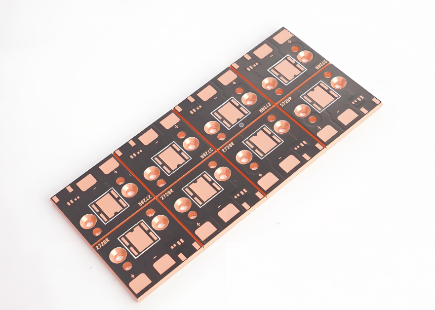
- Optimized Thermal Management Design: Achieving uniform heat dissipation with a temperature difference of ≤3℃ through a layered thermal conductivity structure based on aluminum/copper substrates, extending equipment lifespan.
- Enhanced Material Durability: Utilizing a high-bonding-strength dielectric layer ensures continuous operation without deformation at 85℃, suitable for long-term industrial-grade operation.
- Scalable Cost Control: Integrating standardized processes and flexible production lines, supporting 10K+ batch order delivery, reducing single-board costs by 15% while steadily improving yield.
Welcome to contact us if you have any request for metal core PCB: sales@bestpcbs.com.
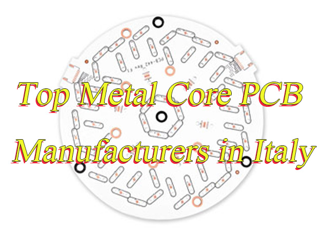
Top Metal Core PCB Manufacturers in Italy
1. Cisel S.r.l.
- Advantages: Over 40 years of PCB manufacturing experience, specializing in high-quality, high-tech Metal Core PCB production, recognized for environmental responsibility in the European market.
- Process Capabilities: Offers single/double-sided, multilayer, flexible, rigid-flex, and aluminum-based (Metal Core) PCBs with through-hole plating technology, applicable to automotive, lighting, industrial, and medical sectors.
- Business: Covers full-range Metal Core PCB manufacturing from prototyping to volume production, including specialized processes like conductive paste boards.
2. CSM Circuiti Stampati Metallizzati S.r.l.
- Advantages: Specializes in specialized PCB products, particularly Metal Core PCBs with superior dimensional stability, mechanical stress resistance, and high thermal dissipation performance.
- Process Capabilities: Produces Metal Core, high-frequency, flexible/rigid-flex, and semi-flexible PCBs using materials such as CEM 3 HT and FR4 HTC.
- Business: Provides PCB prototyping, small-batch to mass production, serving aerospace, automotive, emergency services, and cloud computing industries.
3. Tecnomec S.r.l.
- Advantages: Leading in RF and microwave PCB fields, covering industrial, medical, telecommunications, rail, aerospace, and defense markets.
- Process Capabilities: Rapid multilayer delivery (3-5 days), supports high-frequency materials, flexible/rigid-flex, PTFE, and Metal Core PCBs with microvia, blind/buried via, and high-copper structure technologies.
- Business: Offers specialty PCB manufacturing from rapid prototyping to medium-high volume for Metal Core and metal backplane solutions.
4. SOMACIS S.p.A.
- Advantages: Global high-tech PCB leader with AS9100, NADCAP certifications for aerospace and medical sectors, focused on high-mix low-volume (HMLV) and mission-critical applications.
- Process Capabilities: Manufactures HDI, rigid, rigid-flex, flexible, and Metal Core/metal backplane PCBs up to 50 layers with 25μm line/space capabilities.
- Core Business: Full-value-chain services for high-growth sectors including aerospace, defense, data centers/AI, automotive ADAS, and semiconductor testing.
5. Cistelaier S.p.A.
- Advantages: Part of Finmasi Group’s PCB division, holds EN 9100, IATF 16949, ISO 13485 certifications, with expertise in thermal and power management.
- Process Capabilities: Produces rigid (up to 40 layers), rigid-flex (up to 12 flex layers), HDI, and Metal Core/metal backplane PCBs with thick copper, coin, and heat sink thermal structures.
- Core Business: Full-series PCB solutions from prototyping to volume production for aerospace, defense, rail, automotive, and medical equipment markets.
6. Alba PCB Group
- Advantages: Multiple European production sites (Italy, Germany, Poland, China) offering complete Metal Core PCB solutions from prototyping to volume, with extensive customers in automotive, industrial, defense, lighting, and medical fields.
- Process Capabilities: Covers rigid, rigid-flex, and Metal Core PCBs with high-precision microdrilling (Ø 0.1mm) and advanced surface finishes.
- Business: High-reliability PCBs for critical applications, particularly customized thermal and high-current management solutions.
7. Baselectron S.r.l.
- Advantages: Over 40 years of specialized material PCB experience, produces aluminum-based, Metal Core, and AlluFless (flexible aluminum) PCBs with thermal management and high-speed signal integrity expertise.
- Process Capabilities: Offers single/double-sided, multilayer, rigid-flex, and Metal Core PCBs supporting high-frequency materials (FR4, Teflon, ceramic) and impedance control design.
- Business: Engineering collaboration and rapid prototyping for industrial, automotive, medical, and high-end consumer electronics.
8. Arel Circuiti Stampati S.r.l.
- Advantages: Specialized PCB manufacturing since 1993 with full certification systems, aluminum-based PCBs and Metal Core solutions for high-reliability applications.
- Process Capabilities: Manufactures single-sided, double-sided, multilayer, flexible, rigid-flex, and aluminum-based PCBs with rapid prototyping and medium-high volume support.
- Business: PCB solutions for industrial, energy, transportation, and security systems with emphasis on customization and flexible delivery.
9. Elemaster S.p.A.
- Advantages: EMS provider offering full-cycle services from product planning and design to rapid prototyping, hardware/software development, and industrial production.
- Process Capabilities: Covers HDI, rigid, rigid-flex, and Metal Core PCBs for high-speed, high-frequency, and high-power applications.
- Business: Leading in ODM and EMS for industrial automation, medical, telecommunications, and aerospace sectors.
10. PCB Runner Italia
- Advantages: Italian fast-response PCB manufacturer providing cost-effective Metal Core PCB solutions with flexible ordering from prototyping to medium-high volume.
- Process Capabilities: Produces single-sided, multilayer, impedance-controlled, and Metal Core PCBs with flexible material selection and short lead times.
- Business: Specializes in rapid prototyping and small-batch production for R&D and innovation projects requiring Metal Core thermal PCBs.
How to Evaluate Production Capabilities of Italian Metal Core PCB Manufacturers?
A Comprehensive Guide to Evaluate Production Capabilities of Metal Core PCB Manufacturers in Italy:
1. Technical Capability and Process Level
- Metal Substrate Selection: Verify if manufacturers offer MCPCBs with different substrates such as aluminum (cost-effective) and copper (superior thermal conductivity), with thermal conductivity typically ranging from 1–9 W/m·K.
- Layer Count and Structure: Evaluate experience in single-layer, double-layer, and multi-layer MCPCBs (up to 32 layers), particularly bonding processes between metal substrates, insulating layers, and circuit layers.
- Precision and Minimum Dimensions: Focus on machining precision such as minimum hole diameter (up to 0.10 mm) and line width/spacing (0.15 mm) to ensure compatibility with high-density circuit designs.
2. Production Equipment and Capacity Scale
- Equipment Sophistication: Assess presence of modern production lines including laser drilling, high-precision exposure, and automated surface-mount technology (SMT) to ensure thermal management and electrical performance of MCPCBs.
- Monthly Production Capacity: Understand monthly deliverable MCPCB area (e.g., some manufacturers achieve 500,000 square meters per month) and confirm capability to support both prototyping and medium-to-large volume orders.
3. Quality Certification and Reliability Testing
- International Certifications: Prioritize manufacturers with certifications such as ISO 9001, IATF 16949, UL, and RoHS to ensure compliance with safety and environmental standards.
- Reliability Verification: Inquire about environmental and lifespan testing such as thermal cycling, high-temperature/humidity exposure, and insulation voltage testing to validate long-term stability in high-temperature/high-power scenarios.
4. R&D and Customization Capability
- Material and Process Innovation: Investigate technical expertise in thermal insulating layers (e.g., ceramic-filled polymers) and metal substrate surface treatments (gold plating, ENIG, OSP).
- Design Support: Confirm availability of engineering services including impedance modeling, DFM (Design for Manufacturing), and file conversion to optimize thermal layouts and circuit performance.
5. Supply Chain and Delivery Assurance
- Raw Material Sourcing: Verify stability of key materials like aluminum/copper substrates, copper foils, and thermal interface materials to prevent delays from material shortages.
- Lead Times: Clarify standard lead times for prototypes (typically 5–10 days) and bulk orders (2–4 weeks), and assess capacity for urgent order flexibility.
6. Industry Application Experience
- Sector Case Studies: Prioritize manufacturers with proven success in high-temperature/high-power sectors such as LED lighting, automotive electronics, power modules, and industrial lasers. For example, Italian firm XLED has launched multiple MCPCB-based LED luminaires showcasing local manufacturing strength.
7. Localized Service and Communication
- Language and Technical Support: Italian manufacturers like Cisel and XLED typically offer Italian-language technical coordination to minimize communication barriers.
- After-Sales Service: Evaluate availability of rapid prototyping, failure analysis, and on-site process support for seamless project progression.
8. Cost-Value Balance
- Pricing Transparency: Require itemized quotes based on materials, layers, processes, and quantities to avoid hidden costs.
- Overall Value: Consider not only unit pricing but also quality consistency, on-time delivery rates, and technical service quality to select the most cost-effective long-term partner.
Typical Lead Time for Ordering A Metal Core PCB Sample from Italy
Sample Production Timeline
- Standard aluminum substrate: Approximately 5–7 working days for production completion.
- Copper substrate or structurally complex metal substrates: May require 7–10 working days or longer.
- Rapid prototyping services: Some manufacturers offer expedited options deliverable within 3–4 days.
Shipping and Customs Clearance
- Suppliers within Italy: Local courier typically takes 1–2 working days.
- EU-wide shipments: Transportation time approximately 2–5 working days, accounting for customs clearance.
Key Factors Influencing Cycle Time
- Design complexity: Reduced layer count, trace width/spacing, and smaller hole diameters extend process time.
- Surface treatments: Processes like gold plating or HASL add 1–2 days.
- Engineering verification: Initial collaboration may require 1–2 working days for document review.
- Production scheduling: Manufacturer’s current order backlog affects actual start date.
Recommendations for Italian Buyers
- Early communication: Provide complete Gerber/design files directly to suppliers with explicit “metal substrate sample” requirements.
- Local/EU sourcing: Minimize international logistics and customs risks.
- Expedited options: Inquire about “rush prototyping” services (additional cost applies) with 3–5 day turnaround.
Overall Time Estimate
- Total cycle from order placement to delivery in Italy typically combines production (5–10 days) and shipping (1–5 days), totaling 6–15 working days.
- For precise scheduling, obtain quotes from 2–3 local/European PCB manufacturers with your specific parameters (substrate type, layers, dimensions) to confirm actual lead times.
How to Choose A Reliable Italian Metal Core PCB Manufacturer?
Below Is A Detailed Selection Guide to Italian Metal Core PCB Manufacturers for Your Reference:
1. Evaluate Technical Expertise and Experience
- Confirm the manufacturer’s actual project experience in metal core substrates (aluminum, copper, etc.), particularly cases relevant to your application domains such as LED lighting, power modules, or automotive electronics.
- Inquire about their design support capabilities, including DFM (Design for Manufacturing) reviews and thermal simulation assistance, to ensure your designs can be efficiently converted into mass-producible boards.
2. Verify Quality Certifications and Standards Compliance
- Prioritize manufacturers certified under quality management systems like ISO 9001, ISO 14001, and IATF 16949 (for automotive electronics).
- Check if their products comply with industry standards including IPC-A-600 (PCB acceptance criteria), UL (safety certification), and RoHS (restriction of hazardous substances).
3. Assess Production Equipment and Process Capabilities
- Investigate their dedicated metal core substrate production lines, including high-precision drilling (hole diameters down to 0.2 mm), laser cutting, copper foil lamination, and thermal insulating layer preparation processes.
- Confirm their ability to achieve high thermal conductivity (e.g., 1.0–3.0 W/m·K) in dielectric layers and master surface treatment techniques such as ENIG (electroless nickel immersion gold), OSP (organic solderability preservative), and HASL (hot air solder leveling).
4. Review Material Supply Chain and Inventory Management
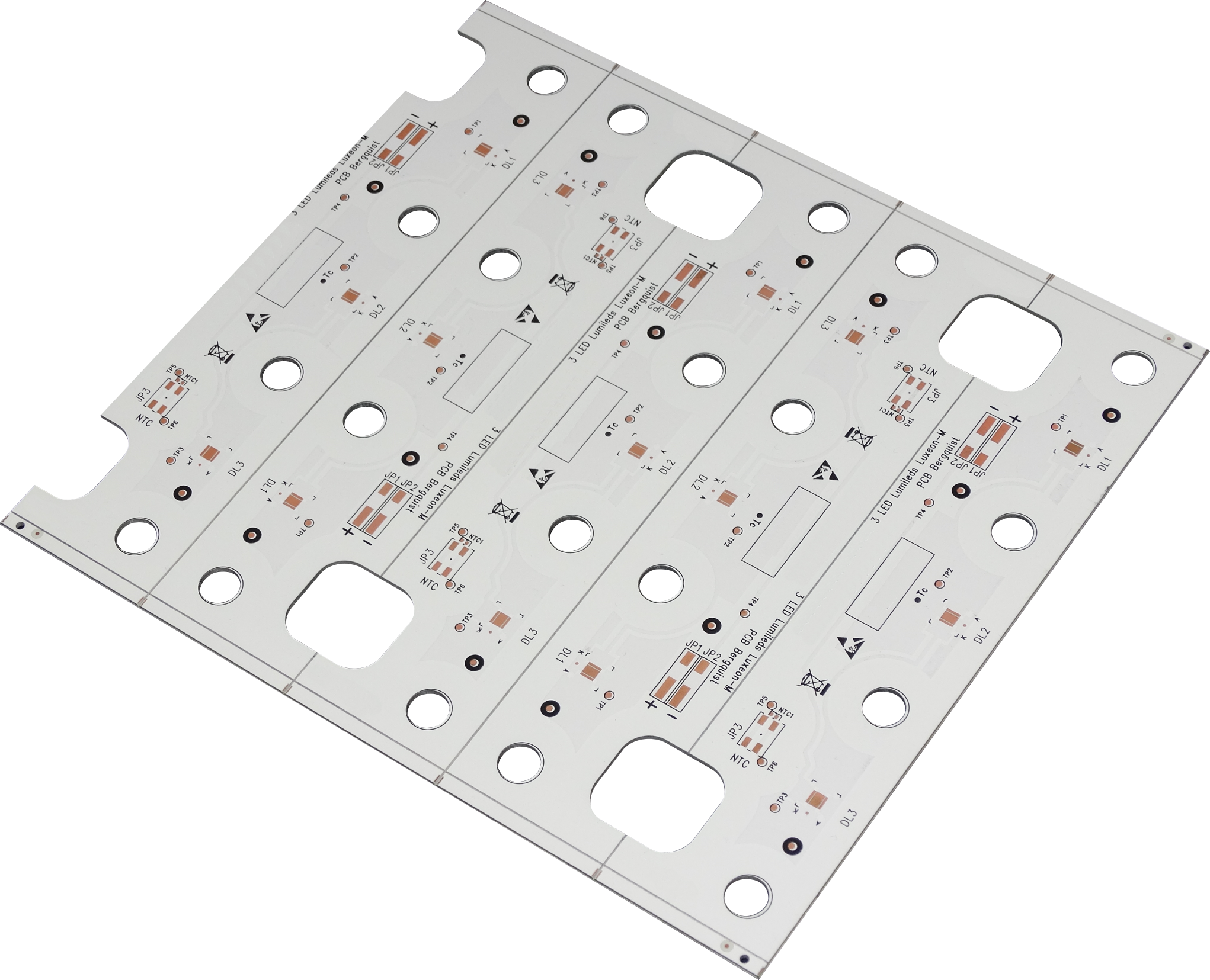
- Ensure they use reputable brand substrates (e.g., Bergquist, VENTEC, BOYU) and can provide certificates of compliance (COC).
- Inquire about inventory levels of commonly used metal core substrates (aluminum, copper) to shorten lead times for prototypes/small batches.
5. Validate Testing and Reliability Assurance
- Request details on their full-process inspection procedures, including electrical testing (flying probe/fixture testing), thermal resistance measurement, impedance control, and thermal shock/aging tests.
- Review reliability reports (e.g., data from high-temperature/humidity and thermal cycling tests) to ensure long-term stability under harsh conditions.
6. Evaluate Delivery Capability and Responsiveness
- Clarify standard lead times (e.g., 5–7 days for prototypes, 2–4 weeks for bulk orders) and expedited options, while confirming if their production capacity can meet your peak demand.
- Examine their logistics partners and export experience to ensure smooth transportation and customs clearance to Italy.
7. Review Contract Terms and After-Sales Support
- Scrutinize contract clauses regarding payment terms, quality guarantees (return/rework policies), confidentiality agreements, and intellectual property protection.
- Confirm the provision of after-sales technical support (e.g., on-site troubleshooting, process optimization advice) and establish long-term collaboration mechanisms.
8. Conduct On-Site or Virtual Factory Audits
- If feasible, arrange on-site visits or virtual inspections to observe cleanroom conditions, equipment maintenance status, and operational compliance.
- Gain insights into actual collaboration experiences through references from existing clients to mitigate risks.
9. Perform Comprehensive Cost Analysis
- When comparing unit prices, consider quality costs (e.g., defect rates, rework time), logistics costs, and currency risks to select suppliers with optimal total cost of ownership (TCO).
Case Studies of Our Italian Metal Core PCB Project
Project Background: An Italian industrial equipment manufacturer plans to develop a new-generation high-power LED driver module for premium outdoor lighting systems. This module must operate continuously under high current (>5 A) in a compact space, requiring PCBs with exceptional thermal performance. The client selected aluminum-based metal core PCBs as the core thermal solution and entrusted us with full-cycle support from design to mass production.
Project Requirements
- Utilize aluminum-based metal core PCB with thermal conductivity ≥2.0 W/m·K.
- Support double-sided routing and plated through-hole (PTH) processes for high-density component layout.
- Maintain PCB surface hotspot temperature below 90°C during continuous operation at 55°C ambient temperature.
- Comply with EU RoHS and CE certification requirements and pass EMC testing.
- Delivery cycle ≤6 weeks, including prototype validation and small-batch production.
Challenges & Difficulties
- Thermal Structure Design: The insulating layer between the aluminum substrate and copper traces must balance high thermal conductivity and high voltage resistance (>2.5 kV) to avoid excessive thermal resistance causing local overheating.
- Hole Metallization Process: Metal substrate through-hole filling and plating are challenging, prone to hole wall separation or thermal pathway interruption.
- Italian Local Supply Chain Integration: Specialty materials (e.g., high-thermal-conductivity dielectric layers) require procurement from outside the EU, increasing costs and time uncertainty due to logistics and tariffs.
- EMC Compatibility: High-power switching circuits generate electromagnetic interference, requiring optimized ground layer and shielding design during layout.
Solutions
- Material Selection: Adopted aluminum-clad copper substrate with ceramic-filled epoxy resin insulation layer, enhancing thermal conductivity to 2.5 W/m·K.
- Structural Design: Implemented large exposed aluminum areas beneath power components, coupled with thermal interface paste for tight thermal coupling with external heatsinks, reducing thermal resistance.
- Process Innovation: Employed laser drilling + electroless copper plating for through-hole metallization, ensuring strong bonding between hole walls and substrate; double-sided traces connected via blind vias to avoid stress risks from full-board PTH.
- Supply Chain Collaboration: Partnered with Italian PCB manufacturer Cisel for local material procurement and rapid prototyping, shortening logistics cycles.
- EMC Countermeasures: Integrated common-mode filters at power inputs and added grounded shielding strips alongside critical signal traces, with pre-layout simulation optimization.
Results
- Thermal Performance Compliance: Achieved stable PCB hotspot temperature of 87°C under 55°C ambient temperature and 5.2 A full load, below the 90°C design threshold.
- Reliability Validation: Passed 1000-hour high-temperature/humidity (85°C/85% RH) aging tests without dielectric layer delamination or hole wall cracking.
- Project Timeline: Delivered first 500-piece batch within 5.5 weeks from design confirmation, meeting client’s market launch window.
Client Feedback: Modules successfully deployed in Milan’s municipal streetlight retrofit project, with zero failures reported over 6 months of operation.
Why Choose EBest Circuit (Best Technology) as Metal Core PCB Manufacturer?
Reasons Why Choose Us As Metal Core PCB Manufacturer:
- Free DFM Analysis: Identifies design defects upfront, reduces design iteration times by 30%, saves 2 weeks of development time on average, and lowers post-modification costs.
- Cost Reduced by Over 30%: Aluminum substrate replacing copper solution, validated by 15 Italian client projects in 2024. Non-critical design simplification cuts material costs by 30%, while layer compression technology (e.g., 4-layer replacing 6-layer) further reduces base costs by 20%.
- 24-Hour Rapid Prototyping: Emergency order response speed ranks top in the industry. Italian clients reduce R&D cycles by 40% on average, accelerating product launch.
- 99.2% On-Time Delivery Rate: Supported by full-year 2024 data, covering 98% of Italian orders, exceeding the industry average of 90% and ensuring supply chain stability.
- Full-Inspection Quality Control: 100% full testing + strict ISO 9001 processes, defect rate ≤0.05%, zero-defect delivery for medical-grade products, compliant with IATF 16949 automotive standards.
- Authoritative Certifications: Holds ISO 9001, ISO 13485 (Medical), RoHS, UL and other international certificates, meeting Italian and EU compliance requirements, reducing client entry barriers.
- Customized Thermal Performance: ≥3W/mK thermal conductivity polyimide dielectric layer, paired with uniform width/thickness dual-sided copper traces, improves thermal distribution uniformity by 30% in real tests, resolving local hotspot issues.
- Via Failure Prevention Process: “Plated through-hole + solder mask” dual protection, passes 1000-cycle -40℃~125℃ thermal shock without failure, vibration/corrosion resistance improved by 50%, extending product life in industrial/automotive environments.
- 19 Years of Industry Experience: Served 500+ Italian clients across automotive, medical, and industrial sectors, accumulating massive localized design case libraries, reducing trial-and-error costs for clients.
- European Localized Response: Dedicated technical support for Italian time zones, average response time of 2 hours, quick demand implementation, seamless communication, and enhanced client experience.

Our Lead Time for Metal Core PCB Prototype
| Layers | Normal Service | Fastest Service |
| 1 | 4 Days | 24 H |
| 2 | 14 Days | 168 H |
| 4 | 21 Days | TBD |
Our MCPCB Manufacturing Capabilities
| Base material: | Copper/ Aluminum Alloy |
| Thermal Conductivity (dielectric layer): | 0.8, 1.0, 1.5, 2.0, 3.0 W/m.K. |
| Board Thickness: | 0.5mm~3.0mm(0.02″~0.12″) |
| Copper thickness: | 0.5 OZ, 1.0 OZ, 2.0 OZ, 3.0 OZ, up to 10 OZ |
| Outline: | Routing, punching, V-Cut |
| Soldermask: | White/Black/Blue/Green/Red Oil |
| Legend/Silkscreen Color: | Black/White |
| Surface finishing: | Immersion Gold, HASL, OSP |
| Max Panel size: | 600*500mm (23.62″*19.68″) |
| Packing: | Vacuum/Plastic bag |
| Samples L/T: | 4~6 Days |
| MP L/T: | 5~7 Days |
How to Get a Quote for Your MCPCB Project?
To obtain a precise quote for your MCPCB project from EBest Circuit (Best Technology), please submit the following essential materials:
- Design Files: Gerber files (including copper, solder mask, silkscreen layers), NC drill files, and assembly drawings in standardized formats (.zip, .rar).
- Material Specifications: Clear requirements for substrate type (e.g., aluminum, copper), core thickness, copper weight (oz), dielectric layer thermal conductivity (≥3W/mK preferred), and surface finish (e.g., HASL, ENIG).
- Quantity & Delivery Timeline: Exact order volume (MOQ or batch size) and required delivery date to align production scheduling.
- Technical Specifications: Critical dimensions, impedance control requirements, via specifications (plated through-hole with solder mask for corrosion resistance), and thermal management needs (e.g., heat sink integration).
- Certification & Compliance: Mention applicable standards (e.g., IATF 16949 for automotive, ISO 13485 for medical) or regulatory requirements (RoHS, REACH) to ensure compliance.
- Special Requests: Any non-standard processes (e.g., laser-cut stencils, selective hard gold plating) or testing requirements (e.g., thermal cycling, vibration resistance).
Welcome to contact us via this email to get a free quote for your MCPCB project: sales@bestpcbs.com.