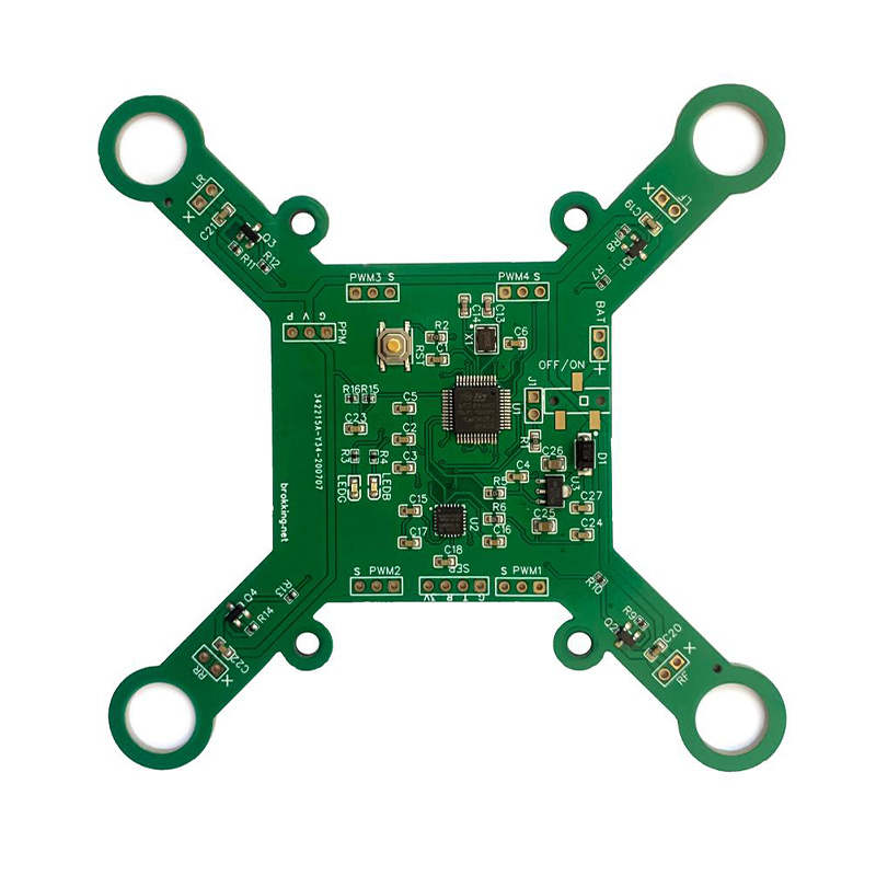
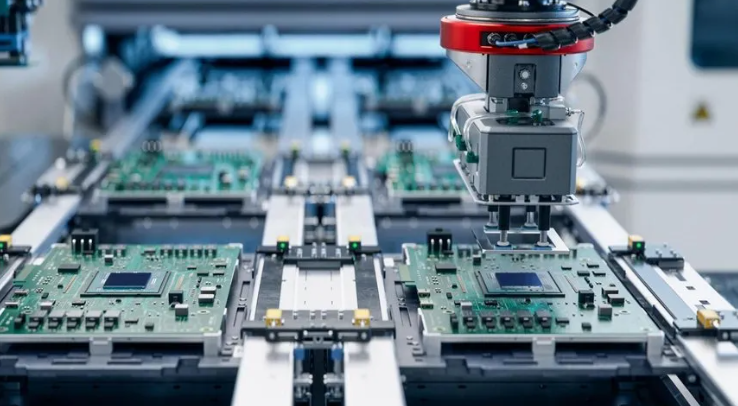
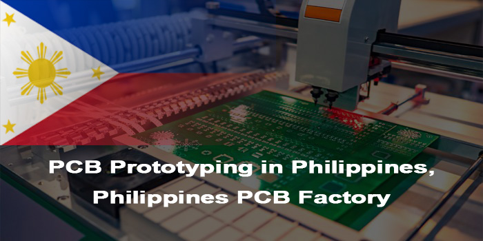
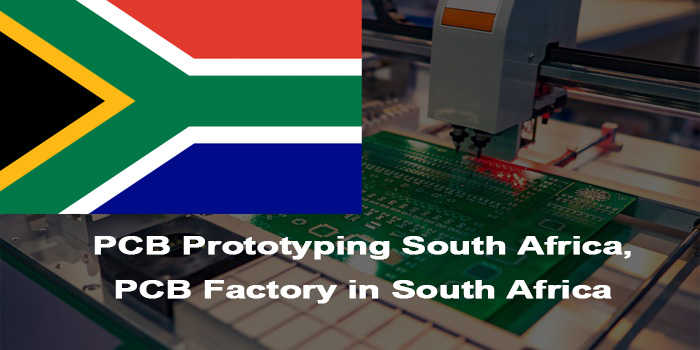
PCB prototyping South Africa serves as a critical link in the nation’s electronics industry, supporting sectors from automotive to renewable energy with tailored circuit board solutions. Local providers combine regional market insights with technical capabilities to deliver prototypes that align with specific application needs. PCB prototyping South Africa also benefits from government re-industrialization initiatives, fostering closer collaboration between service providers and end-users for faster design iterations and reduced supply chain risks.
Why Choose PCB prototyping South Africa?
- Proximity-driven collaboration enables real-time communication, reducing design revision delays by 30% compared to offshore services.
- Compliance with local industrial policies supports preferential procurement for automotive and aerospace sectors.
- Faster shipping within the region, with domestic delivery taking 1-3 business days versus 7-14 days for international prototypes.
- Access to industry-specific expertise, particularly for renewable energy and industrial automation applications.
- Flexible small-batch prototyping options, catering to low-volume needs without excessive minimum order requirements.
- Alignment with regional quality standards and certifications relevant to African markets.
- Reduced import duties and logistics costs, lowering overall prototype investment by 15-20%.
- Local technical support for post-prototyping adjustments, minimizing downtime in product development cycles.
Quality Certifications of PCB Prototyping South Africa
- RoHS 2.0 (2011/65/EU) Certification: Ensures compliance with restricted hazardous substances limits, including 0.1% maximum for lead, mercury, hexavalent chromium, PBB and PBDE, and 0.01% for cadmium.
- UL Certification for Laminates: Covers standard FR-4, high-Tg FR-4, and PTFE materials, validating flame retardancy and safety performance for PCB prototyping in South Africa.
- ISO 9001:2000 Quality Management System Certification: Adopted by leading local manufacturers to standardize production processes and quality control.
- IPC Certification: Compliant with IPC-2221 standards, providing formal validation for PCB design and manufacturing consistency in South Africa PCB prototype production.
- NPS RoHS Certification: Issued by European NPS environmental certification body, facilitating market access for PCB prototype South Africa products exported to the EU.
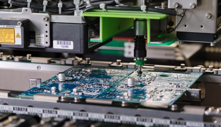
Top PCB Factory in South Africa for Prototyping
| Company Name | Main Business | Core Advantages | Process Capabilities | Lead Time |
| EBest Circuit Co., Limited(Best Technology Circuit Co., Limited) | PCB prototyping, mass production, SMT assembly | Advanced HDI technology, 1-32 layer capability, global supply chain | Blind/buried vias, impedance control, 30oz heavy copper, 0.15mm ultra-thin boards | 24hrs for 2-layer prototype, 3-5 days for multilayer |
| ICAPE Trax | Rigid PCB prototyping, small to medium runs | First SA PCB manufacturer with ISO 9001:2000, Cape Town-based | 1-18 layer FR4, ENIG/HASL finish, RF PCB capability | 3 days (PTH), 5 days (4-layer), 7 days (6-layer) |
| Pro Circuit | PCB fabrication, SMT assembly, turnkey solutions | 33 years of local experience, cross-industry expertise | 1-16 layer rigid PCBs, functional testing | 14-20 workdays, 10-14 workdays for rush orders |
| Master Circuits | Rigid/flexible/rigid-flex PCB manufacturing | Durban-based, high-layer count capability | Up to 60 layers, FR4/aluminum substrates | 10-15 workdays for prototypes |
| Cirtech Electronics (Pty) Ltd | PCB prototyping, high-volume production | Local market expertise, versatile production scales | Small-run to large-scale, precision manufacturing | 8-12 workdays for prototypes |
| Expando Works (Pty) Ltd | Flexible/rigid PCB prototyping, industrial supply | Aerospace and defense certification, aluminum/copper substrates | Up to 20 layers, flexible circuits, FR4/aluminum materials | 7-10 workdays for prototypes |
How to Choose the Best PCB Prototype Service South Africa?
A Selection Guide to Best PCB Prototype Service South Africa:
- Start with data intake rigor: A capable PCB factory in South Africa will review Gerber, drill, stackup, and fabrication notes before releasing the job to production. Early CAM questions signal process control. Silence usually means assumptions.
- Confirm electrical test coverage: Ask whether flying probe testing is standard for prototypes and what percentage of nets are covered. Full netlist verification reduces the chance of chasing faults that originate in fabrication, not the circuit.
- Evaluate tolerance transparency: Reliable PCB prototyping in South Africa suppliers publish or clearly state achievable limits for trace width, spacing, annular ring, solder mask alignment, and finished thickness.
- Verify material and finish availability: Check which laminates are stocked locally and which finishes are routine. ENIG, lead free HASL, and controlled Tg materials should be standard, not special requests that extend lead time.
- Assess communication speed and clarity: The best PCB prototype South Africa experience is defined by fast, specific feedback. Look for annotated screenshots, marked up stackups, and direct recommendations rather than generic comments.
- Compare lead time by board complexity: Strong suppliers differentiate turnaround by layer count and technology. Published prototype timelines for two, four, and six layer boards indicate mature planning and realistic capacity control.
- Review inspection and acceptance criteria: Confirm alignment to IPC A 600 for visual quality and IPC 6012 intent for performance. This avoids disputes where boards pass electrical test but fail cosmetic or reliability expectations.
- Consider iteration efficiency, not single build cost: In PCB prototyping South Africa, the lowest quote is rarely the lowest total cost. Faster clarification, fewer re spins, and predictable delivery usually outweigh small price differences.
- Check scalability beyond the prototype: Even for early builds, confirm whether the same South Africa PCB factory can support pilot and volume runs. Consistency across stages reduces risk when designs stabilize.

Production Capabilities of PCB Prototyping South Africa
| Capability Category | Technical Specifications |
| Layer Count Capacity | Rigid PCBs: 1-60 layers; Flexible/Rigid-Flex: 1-20 layers; HDI: 3+C+3 structure (limited providers) |
| Line Width & Spacing | Minimum line width/space: 3.0mil (0.076mm); Tolerance: ±10% for lines ≤0.2mm |
| Drilling Capability | Mechanical drill: ≥4mil (0.1mm), tolerance ±0.05mm; Laser drill: ≥4mil, tolerance ±0.02mm; Max aspect ratio 40:1 |
| Copper Thickness & Plating | Copper thickness: 0.25-30oz; Hole wall coverage ≥98%; Heavy copper plating up to 30oz for power boards |
| Substrate & Impedance Control | Substrates: FR-4, high-Tg FR-4, PTFE, aluminum; Impedance tolerance: ±5% (RF boards), ±10% (general boards) |
| Surface Finishing | ENIG (0.05-0.1μm gold), HASL (leaded/lead-free), Immersion Tin, Immersion Silver, Gold Finger Plating |
Lead Time for PCB Prototyping South Africa
| Prototype Type | Standard Lead Time | Rush Lead Time |
| 1-2 Layer Rigid (PTH) | 3-5 workdays | 24-48hrs |
| 4-6 Layer Rigid | 5-7 workdays | 3-4 workdays |
| 8-18 Layer Rigid | 7-10 workdays | 5-6 workdays |
| Flexible/Rigid-Flex | 10-15 workdays | 7-8 workdays |
How Much Does Prototype PCB South Africa Cost?
Origination fees form the base cost for PCB prototyping South Africa, varying by board type. Single-sided prototypes have origination fees of $30-$60, while double-sided options range from $50-$150. These fees cover tooling, setup, and design file verification.
Per-unit costs depend on quantity and complexity. For 1-10 units of 2-layer FR4 prototypes (100x100mm), per-unit pricing is $8-$15. For 4-layer prototypes of the same size, per-unit costs increase to $12-$22. High-layer count (10+ layers) or specialty materials (PTFE, aluminum) add $5-$15 per unit.
Rush service premiums typically add 30-50% to the total cost. For example, a 2-layer prototype with standard lead time of $100 becomes $130-$150 for 24hr turnaround. Domestic shipping costs $5-$15, with overnight delivery adding $10-$20.
Future Challenges for PCB Prototyping in South Africa
- Limited advanced technology adoption, with few local manufacturers offering HDI and microvia capabilities for high-density designs.
- Higher material costs compared to global hubs, driven by import dependencies for specialty laminates like Rogers.
- Skilled labor shortages, particularly in precision plating and impedance control calibration.
- Capacity constraints for high-volume prototyping, as most South Africa PCB factory focus on small to medium runs.
- Global competition from low-cost offshore providers, pressuring local pricing while maintaining quality standards.
- Slow adoption of Industry 4.0 technologies, leading to lower process efficiency than international counterparts.
- Volatility in import duties for equipment and materials, increasing cost unpredictability.
FAQs of PCB prototyping South Africa
Q1: Why do prototype quotes vary so much between local and overseas options for the same Gerbers?
A1: The main difference is pooling versus dedicated processing. Local PCB prototyping in South Africa is often priced as a custom job with higher fixed handling cost, while pooling services amortize setup across many orders. Buyers in South Africa have reported local per board quotes far above pooled overseas pricing for small runs.
Q2: Why does delivery feel slow even when the factory time looks fast?
A2: The hidden variable is logistics. Overseas options can show fast factory time, but the delivery clock is dominated by shipping legs and customs timing. When you choose PCB prototyping South Africa, the goal is to reduce this variability by keeping the critical path domestic.
Q3: What causes the most prototype re spins after the first build?
A3: Missing fabrication notes and unclear constraints. When stackup intent, impedance needs, or hole tolerances are not explicit, the factory will default to standard rules that may not match your electrical or mechanical expectation. Community discussions about prototype confidence often emphasize iterating with better preparation and verification rather than hoping the first build is perfect.
Q4: Why do boards sometimes come back functional but still fail inspection expectations?
A4: Electrical function does not guarantee workmanship acceptability. Align on inspection criteria early, usually with IPC A 600 visuals plus performance expectations such as IPC 6012 class intent.
Q5: How can you shorten turnaround without increasing the risk of defects?
A5: Reduce avoidable complexity before you pay for speed. The cleanest path is a strong DFM pass, minimized drill counts where possible, realistic trace and space, and clear acceptance criteria. Fast turnaround conversations repeatedly highlight that data quality and manufacturability are what unlock speed without gambling on yield.