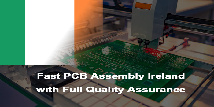
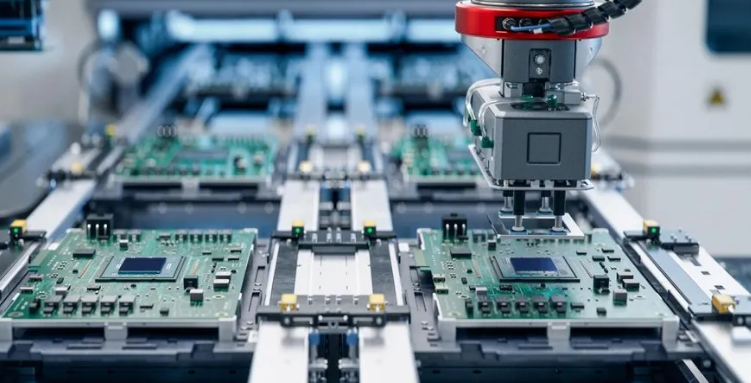
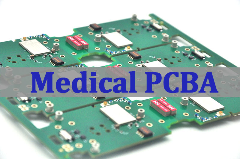
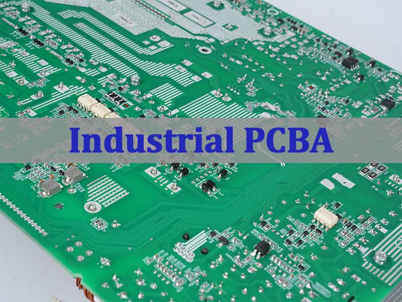
Industrial PCBA forms the operational core of modern industrial equipment, translating complex electronic designs into reliable, functional hardware that drives automation and control. This article explores the evolving landscape for Industrial PCBA manufacturers serving the Brazilian market, analyzing key trends, engineering challenges, and the strategic considerations between local and overseas sourcing, culminating in a guide for selecting the right manufacturing partner.
What are the most common pain points that delay or compromise industrial PCBA assembly projects?
- Inconsistent quality and reliability in harsh plant environments, leading to premature field failures.
- Unpredictable lead times and delivery delays from suppliers, disrupting production schedules.
- Hidden costs and lack of cost transparency, eroding project budgets after initial industrial PCBA quotes.
- Limited access to specialized engineering support for industrial control PCBA or industrial robotics PCBA design challenges.
- Supply chain fragility and poor component traceability, risking production stoppages and complicating lifecycle management.
The solution lies in selecting a industrial PCBA manufacturer whose processes are specifically engineered to mitigate these exact risks.
- Implement Rigorous, Process-Driven Quality Gates: Enforce standards like IPC Class 3 and ISO 9001/16949 at every stage, from industrial PCBA prototyping to volume runs.
- Guarantee Supply Chain & Production Visibility: Provide transparent scheduling and real-time updates to ensure on-time delivery for industrial PCBA assembly services.
- Offer Detailed, Upfront Cost Analysis: Break down all NRE, tooling, and unit costs clearly to avoid surprises and support budget planning.
- Provide Dedicated DFM & Engineering Support: Assign experts to collaborate on thermal design, component selection, and layout for high-performance PCBA for industrial equipment.
- Establish a Robust, Documented Supply Chain: Leverage strong supplier relationships and full component traceability to ensure resilience and support long lifecycle requirements.
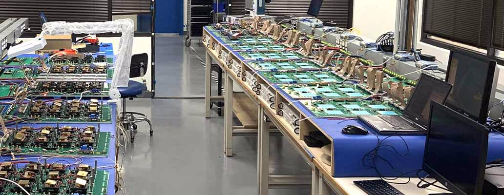
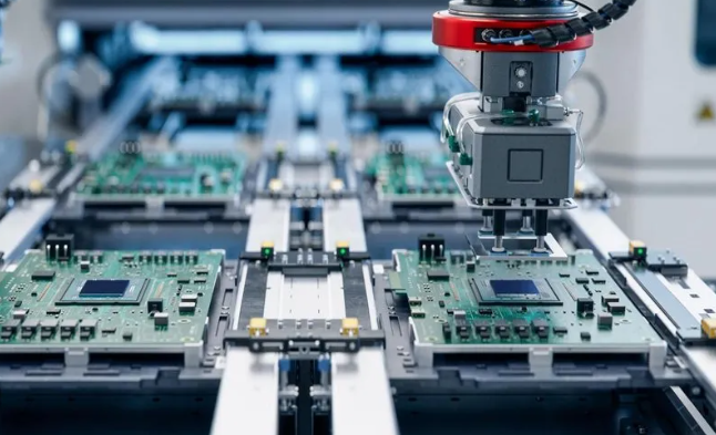
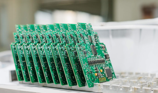
EBest Circuit (Best Technology) is a dedicated industrial electronics PCBA manufacturer supporting global industrial markets, including Brazil, with engineering-driven and cost-efficient manufacturing solutions. By leveraging the capabilities of our China-based industrial PCBA facilities, we provide a seamless one-stop service for industrial electronics — from early-stage prototyping and design optimization to stable, scalable mass production. Rather than focusing only on assembly, our team works closely with customers to develop practical custom industrial PCBA solutions that balance performance, reliability, and long-term supply stability, meeting the expectations of industrial automation projects worldwide. For project discussions or quotation support, please contact sales@bestpcbs.com.
How Industrial Automation Growth In Brazil Is Reshaping Demand For Industrial PCBA Manufacturers?
The rapid expansion of industrial automation in Brazil is fundamentally altering the specifications and expectations for Industrial PCBA manufacturers. Demand is shifting from simple, standard boards to complex, intelligent, and ruggedized assemblies.
- Demand for Higher Complexity: Automation drives the need for boards with more processing power, connectivity (IoT), and sophisticated sensor integration.
- Emphasis on Ruggedization: Equipment in mining, agriculture, and manufacturing requires PCBA that can withstand vibration, humidity, and wide temperature swings.
- Need for Customization: Off-the-shelf solutions fall short. There is growing demand for custom industrial PCBA solutions tailored to specific machinery and processes.
- Pressure on Reliability & Uptime: Automated lines cannot tolerate frequent failures. PCBA must achieve exceptional Mean Time Between Failures (MTBF).
- Integration with Legacy Systems: New control boards often need to communicate with older industrial networks, requiring specialized interface design.
This growth creates a lucrative but demanding market for suppliers who can deliver not just assembly, but comprehensive industrial PCBA solutions that are robust, smart, and fully integrated.
Why Many Brazil OEMs Source From China Industrial PCBA Instead Of Local EMS Providers?
While local EMS providers offer geographical proximity, many Brazilian OEMs choose China industrial PCBA partners for stronger scalability, broader engineering resources, and more stable delivery performance — especially in industrial PCBA manufacturing where long-term reliability and supply-chain efficiency matter more than simple location advantages.
| Consideration | Sourcing From Local EMS (Brazil) | Sourcing From Specialized China PCBA Manufacturer |
|---|---|---|
| Cost Structure | Higher labor cost | Scaled cost efficiency |
| Technical Ecosystem | Limited specialization | Deep supplier network |
| Prototyping Agility | Slower iteration | Fast prototype cycles |
| High-Mix Capability | Standard builds | Complex builds ready |
| Lead Time Reality | Short shipping | Fast sourcing + build |
| Long-Term Cost Vision | Unit-price focus | TCO-driven approach |
Many engineers assume local EMS automatically means faster delivery. In reality, lead time is often determined by component sourcing speed and engineering workflow rather than distance alone.
- Local EMS may shorten final logistics but can face longer material preparation cycles.
- China industrial PCBA manufacturers often reduce overall schedule through faster sourcing, rapid DFM feedback, and parallel manufacturing processes.
- For industrial control board PCBA and automation projects, total turnaround time is frequently influenced more by engineering responsiveness than by shipping distance.
Because of this, many Brazil OEM teams evaluate partners based on total project lead time rather than geographic proximity alone, balancing sourcing speed, production stability, and long-term scalability.
Engineering Challenges Behind Industrial Control Equipment PCBA In Harsh Environments
Designing industrial control equipment PCBA for Brazilian industrial settings—such as sugarcane mills, mining operations, or offshore platforms—presents unique engineering hurdles that go beyond standard commercial design.
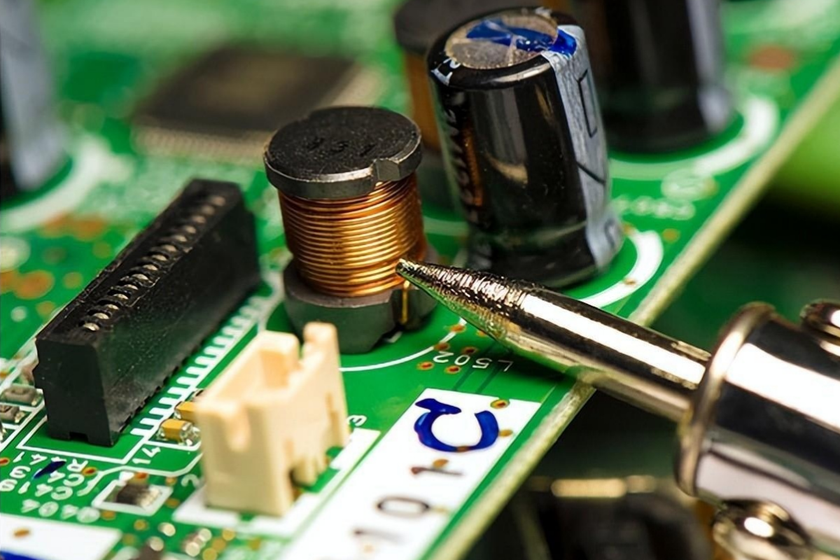
- Environmental Contamination: Dust, moisture, and chemical vapors necessitate conformal coating (using an industrial coating machine for PCBA) and sealed enclosures.
- Thermal Stress: High ambient temperatures and poor ventilation require meticulous thermal management via heatsinks, layout optimization, and derating.
- Mechanical Stress: Continuous vibration and shock demand secure mounting, strategic underfilling of BGAs, and the use of rigid flexible PCB PCBA for industrial applications where movement is present.
- Electrical Noise & ESD: Noisy motor drives and high-power equipment create EMI/RFI challenges, requiring careful grounding, shielding, and filtering circuit design.
- Longevity & Obsolescence: Industrial machines have decades-long lifecycles. Designing for component longevity and managing obsolescence are critical planning activities.
Overcoming these challenges is not optional; it is fundamental to creating a reliable industrial control PCBA that will perform consistently in the field, minimizing downtime and maintenance costs.
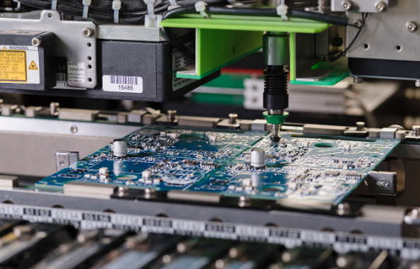
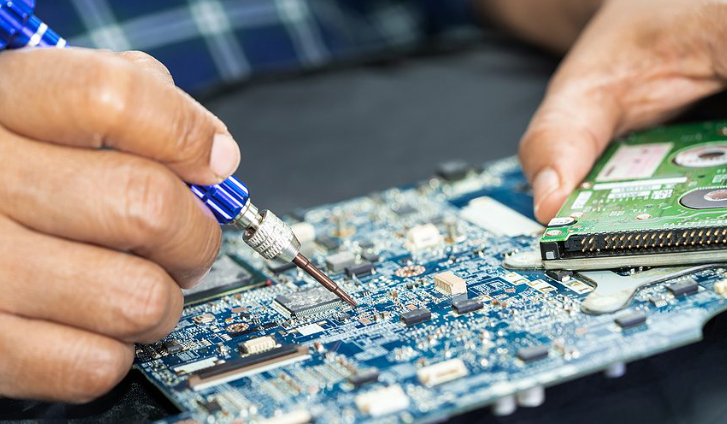
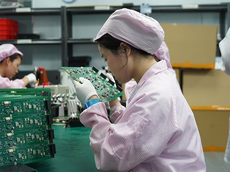
From Prototype To Volume How Industrial Control Board PCBA Prototype Assembly Reduces Risk?
The industrial control board PCBA prototype assembly phase is a critical risk-mitigation step, not merely a first article check. A well-executed prototype run validates the entire production pathway before significant capital is committed.
- Design for Manufacturability (DFM) Validation: Catches layout issues that could cause assembly defects or reliability problems in volume.
- Component Sourcing & Compatibility Check: Verifies real-world component performance and availability within the supply chain.
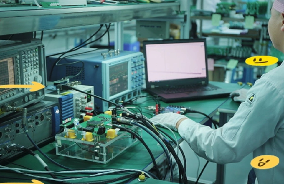
- Functional & Environmental Testing: Allows the PCBA to be tested under simulated harsh conditions (thermal cycling, vibration) before field deployment.
- Process Proofing: Establishes the assembly process, solder profiles, and inspection criteria that will be scaled for volume.
- Cost Refinement: Provides accurate data to refine the final industrial PCBA quotes for volume production.
Skipping or rushing the prototype phase for industrial control board PCBA often leads to costly re-spins, delayed launches, and quality issues in the field. It is an essential investment in project success.
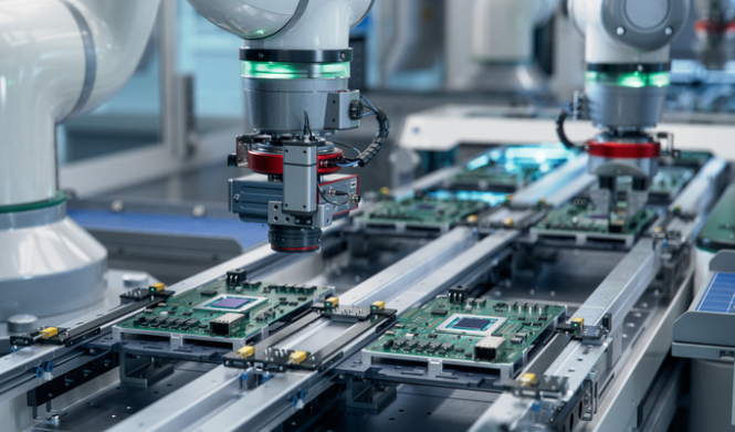
Thermal Design And Reliability Considerations For Industrial Robotics PCBA Applications
Industrial robotics PCBA operates at the extreme end of performance and environmental demand. Servo drives, motor controllers, and vision systems generate significant heat in confined spaces, making thermal management paramount.
Key Design Considerations:
- Power Density Mapping: Identify high-heat components (MOSFETs, FPGAs, processors) early in the layout phase.
- Thermal Interface Materials (TIMs): Select appropriate thermal pads, greases, or phase-change materials to efficiently transfer heat to enclosures or heatsinks.
- Strategic Layer Stack-up: Use dedicated power and ground planes to spread heat and use internal layers as thermal conduits.
- Forced Air vs. Conduction Cooling: Decide based on the robot’s architecture. Joint controller PCBA may rely on conduction to the robot arm structure itself.
- Reliability Modeling: Use formulas like the Arrhenius equation to model and test lifespan under elevated temperature stress, ensuring the PCBA for industrial controller meets its target MTBF.
Failure to adequately address thermal design is a leading cause of failure in high-performance PCBA for industrial equipment like robotics, directly impacting speed, precision, and uptime.
Why Industrial Electronics PCBA Manufacturers Focus On Traceability And Long Lifecycle Support?
For an industrial electronics PCBA manufacturer, the commitment extends far beyond the point of sale. Traceability and long lifecycle support are non-negotiable services for industrial clients.
- Component Traceability: Full lot-code tracking for every IC and critical component is essential for rapid root-cause analysis if a field issue arises and for managing recalls.
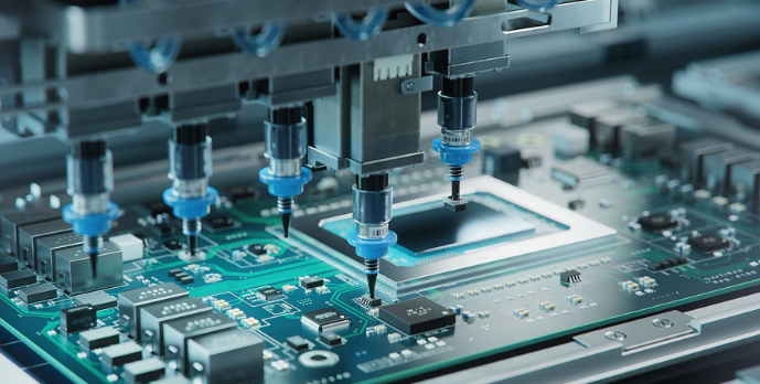
- Production Data Logging: Storing data from solder paste inspection (SPI), automated optical inspection (AOI), and in-circuit test (ICT) for each board serial number.
- Obsolescence Management: Proactive notification of component end-of-life (EOL) and offering redesign or last-time-buy (LTB) services to keep production lines running for 10+ years.
- Archival of Design & Process Files: Secure, long-term storage of Gerbers, BOMs, assembly drawings, and test procedures to enable reproduction years later.
- Repair & Return Support: Maintaining the capability and spare parts to repair legacy boards, supporting the entire lifecycle of the industrial asset.
This focus transforms a manufacturer from a simple board assembler into a true long-term partner for oem customers in ems industry.
Comparing OEM Industrial Control PCBA And Standard EMS Manufacturing Models
Choosing between a partner focused on OEM industrial control PCBA and a standard EMS provider is a strategic decision with significant implications.
| Aspect | OEM Industrial Control PCBA Partner | Standard EMS Provider |
|---|---|---|
| Core Focus | Industrial control specialization | General electronics focus |
| Engineering Engagement | Deep engineering support | Basic DFM feedback |
| Quality Mindset | Reliability-driven builds | Standard IPC Class 2 |
| Supply Chain Strategy | Long-lifecycle components | Cost-driven sourcing |
| Value Proposition | TCO and stability | Lowest unit price |
For industrial equipment PCBA company projects, a specialized partner model often delivers stronger long-term reliability, lower operational risk, and more predictable lifecycle costs.
Why Choose EBest Circuit (Best Technology) for Industrial Robotics PCBA Fabrication?
Selecting EBest Circuit for your industrial robotics PCBA fabrication consolidates the advantages discussed throughout this article. We specialize in the niche where high complexity meets harsh environment requirements.
- Proven Harsh-Environment Expertise: Our processes are fine-tuned for the thermal, mechanical, and environmental demands of robotics, ensuring robust precision PCBA assembly for industry.
- Seamless Prototype-to-Volume Bridge: We mitigate risk through disciplined industrial PCBA prototyping, ensuring a smooth, scalable transition to volume production without surprises.
- Dedicated Engineering Partnership: We act as an extension of your team, providing the deep industrial control PCBA design support needed to solve thermal, signal integrity, and power challenges.
- China-Based Efficiency with Global Standards: You benefit from competitive industrial PCBA manufacturing costs and a vast component ecosystem, while we deliver quality certified to IPC Class 3 and ISO16949 approved processes.
- Full Lifecycle Commitment: We build and support your PCBA boards for OEM EMS industry customers with complete traceability and long-term obsolescence management, protecting your investment.
In a nutshell, industrial PCBA is the critical, intelligent backbone that powers innovation and efficiency across Brazil’s growing industrial sectors. This article has examined the market dynamics, engineering imperatives, and strategic sourcing decisions that define success in procuring reliable, high-performance industrial PCBA electronics. EBest Circuit (Best Technology) is positioned as a reliable industrial robotics PCBA partner, offering Brazilian OEMs access to custom industrial PCBA solutions built on a foundation of quality, reliability, and deep industrial expertise.To discuss your industrial PCBA assembly project, please contact us at sales@bestpcbs.com.
FAQs about Industrial PCBA
Why Do Industrial PCBA Prototype Runs Often Fail Even When The Design Looks Correct?
Even flawless schematics can hide manufacturing pitfalls. Prototype failures often uncover DFM issues (e.g., thermal reliefs, solder mask slivers), component sourcing/quality problems, or undetected signal integrity/power distribution flaws that only manifest when physically assembled and tested under load.
Is China Industrial PCBA Always Cheaper Than Local Manufacturing For Industrial Projects?
While unit cost is often lower, the true comparison is Total Cost of Ownership (TCO). For complex, reliability-critical industrial PCBA solutions, China’s combination of advanced technical expertise, supply chain scale, and focused industrial experience frequently results in a lower TCO despite logistics, when factoring in superior quality, reduced field failures, and better scalability.
Does IPC Class 3 Really Improve Reliability For Industrial Control PCBA?
Absolutely. IPC Class 3 defines the most stringent acceptance criteria for workmanship, targeting “high-performance electronic products where continued performance or performance on demand is critical.” For industrial control PCBA in harsh, inaccessible environments where failure is unacceptable, manufacturing to Class 3 standards is a fundamental requirement for achieving the necessary reliability and longevity.