Solder resist is a key material used in PCB (Printed Circuit Board) manufacturing to protect the circuit traces. This thin layer, typically green in color, ensures that solder only adheres to specific areas during the assembly process. Without solder resist, PCBs could suffer from short circuits, poor connections, and overall performance issues.
What is a Solder Resist?
Solder resist, sometimes known as a solder mask, is a protective layer applied to the surface of a PCB. In essence, solder resist is an insulation ink, its primary function is to prevent the solder from flowing onto unwanted areas during the soldering process. By applying a layer of solder resist, manufacturers can ensure the quality and reliability of the board’s electrical connections.
The solder resist material protects the copper traces, ensuring that the PCB functions correctly by providing an insulated surface. It also enhances the overall durability of the PCB by preventing oxidation or damage to the copper.
Types of Solder Resist
There are several types of solder resist materials, each offering different benefits for specific manufacturing processes. Each type of solder resist serves its purpose based on the complexity of the PCB design and the manufacturing process involved. The most commonly used solder resist types are:
- Liquid Solder Resist: Applied using a spray or traditional screen printing method, this type is the most popular and offers ease of application. In generally, it is a default types of soler resist if there are no any special requirements from customers.
- Dry Film Solder Resist: This is a laminated material that is applied to the board before exposure to ultraviolet (UV) light. After exposure, the unwanted parts of the resist are washed away.
- Photo-sensitive Solder Resist: It is a special variant that reacts to UV light, making it ideal for highly detailed, small-scale PCB designs.
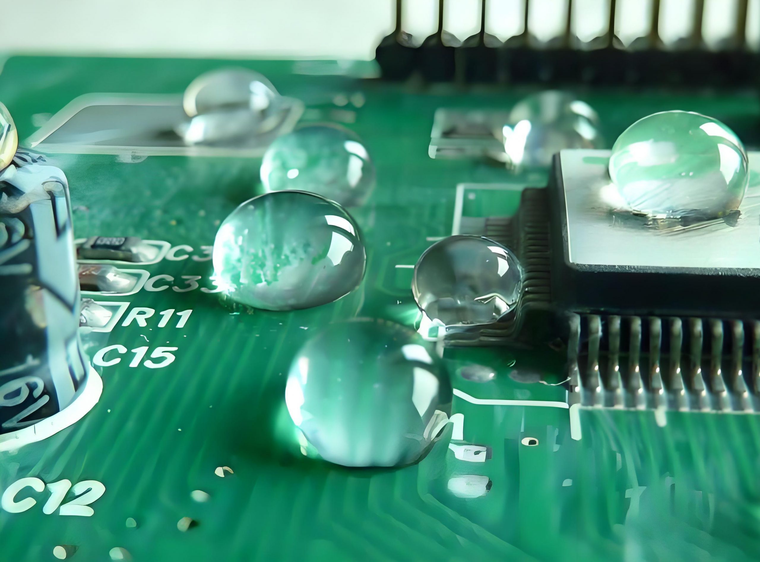
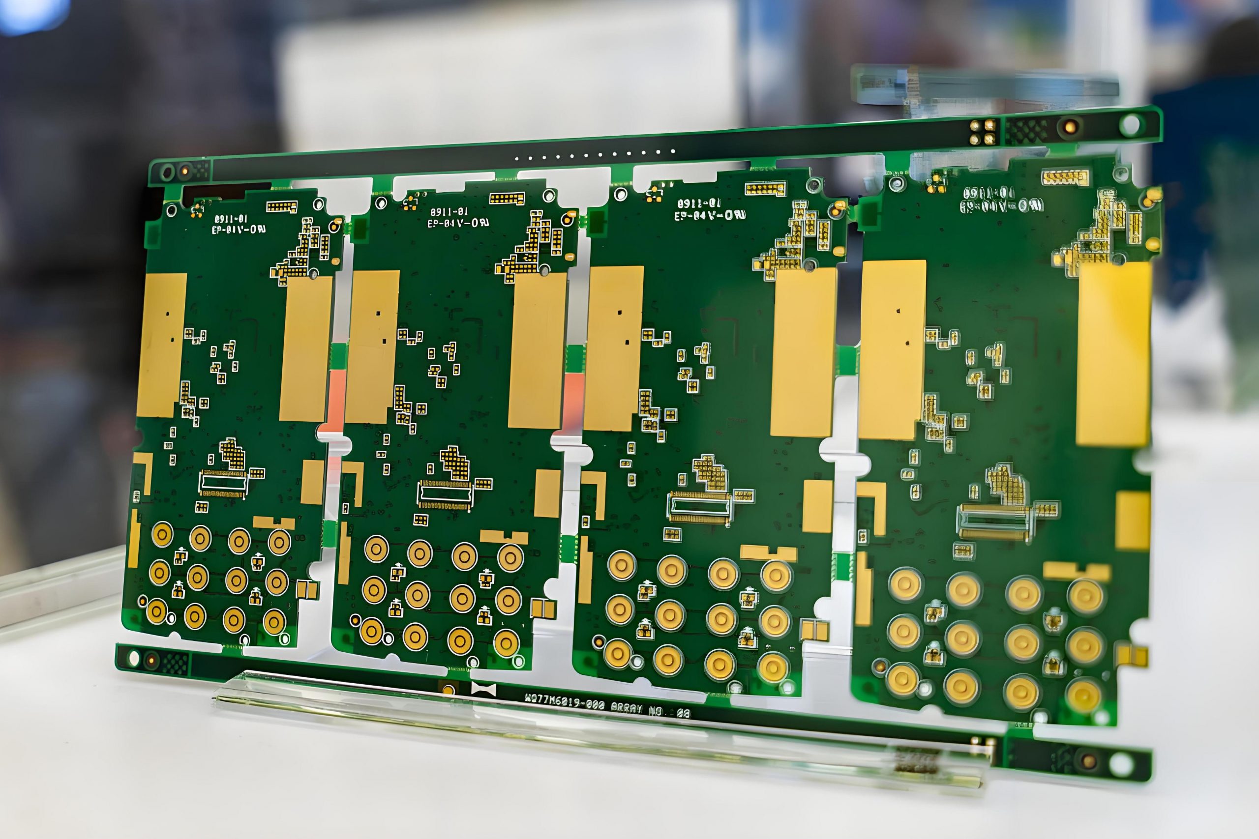
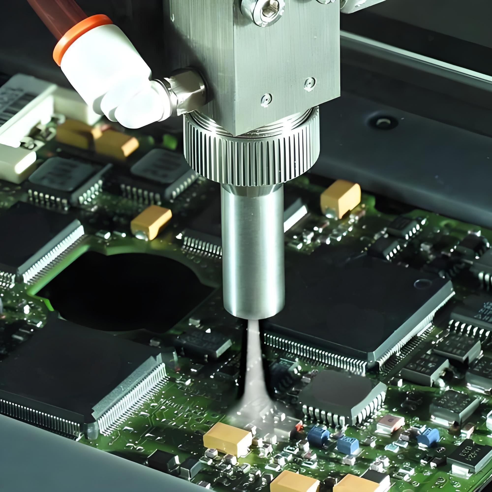
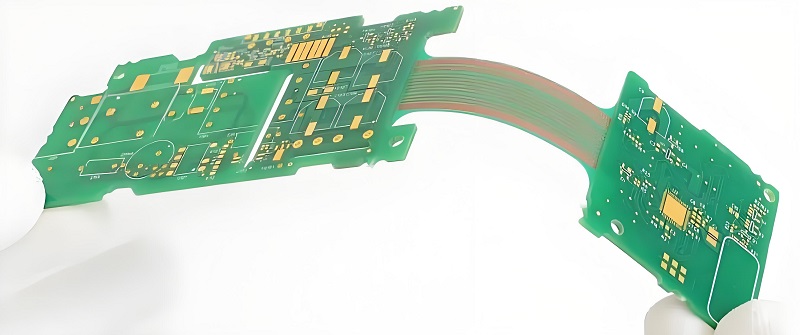
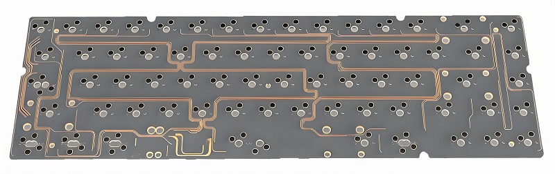
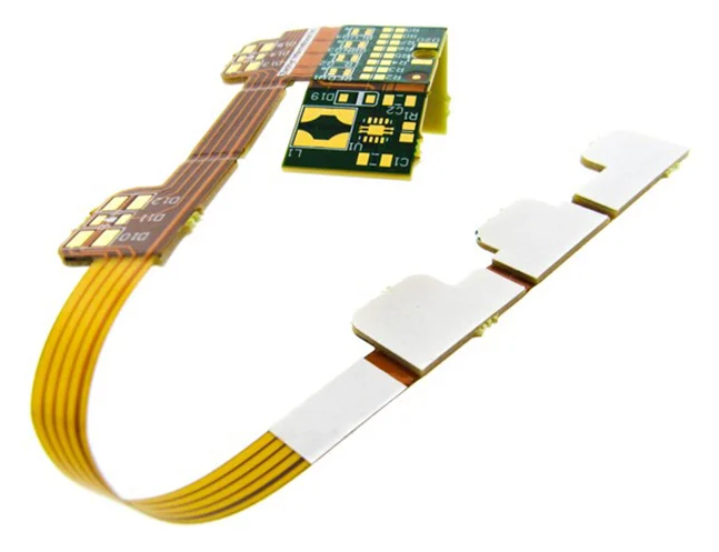
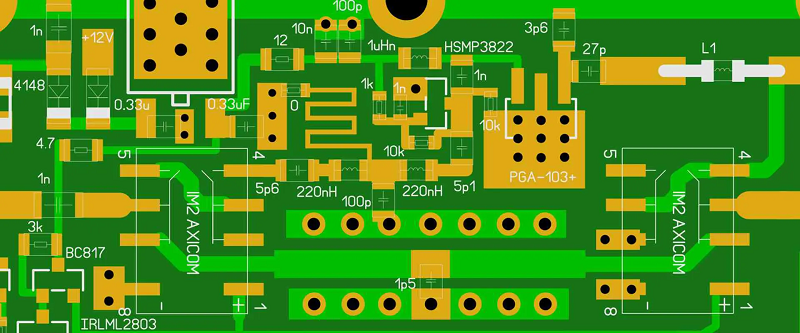
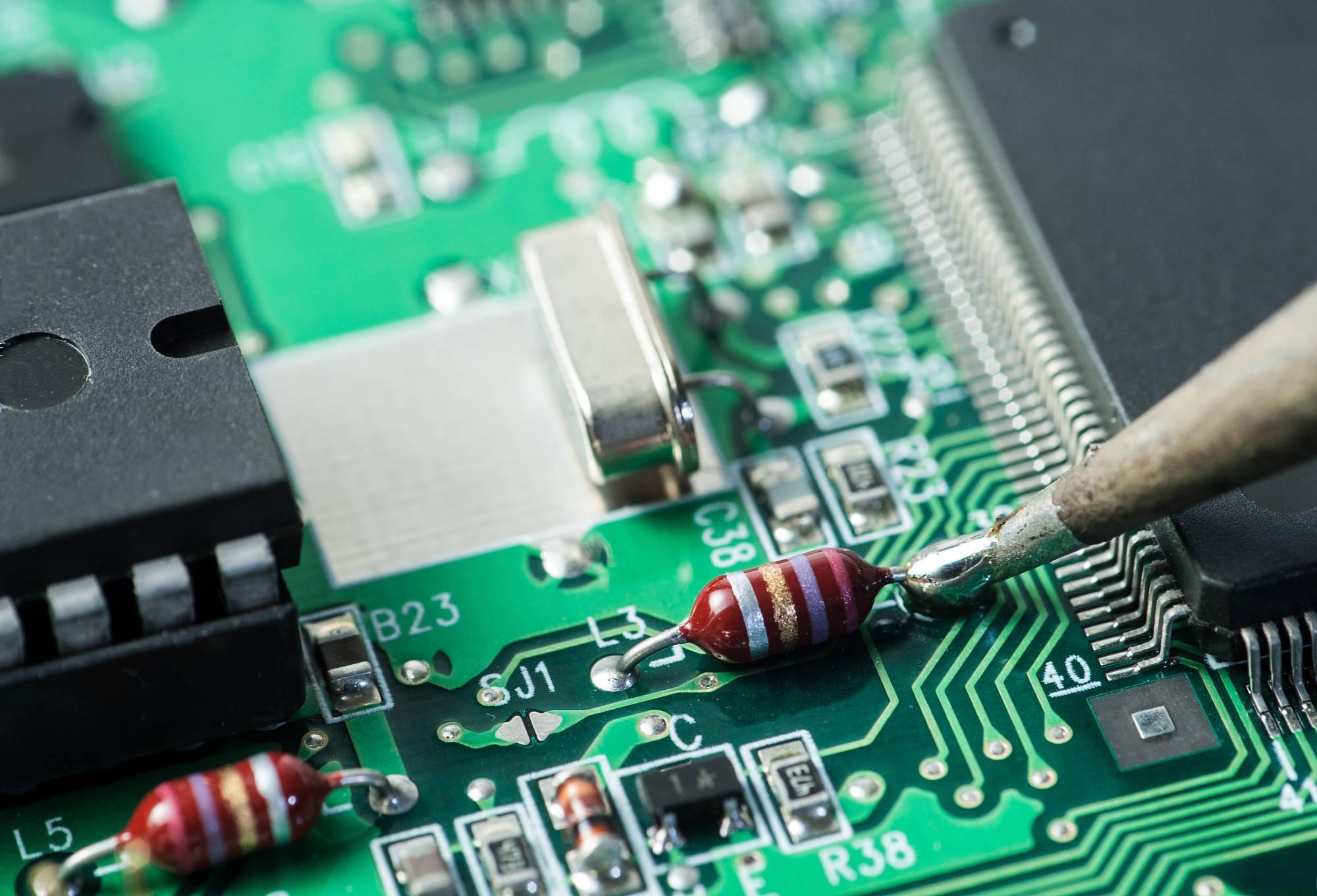
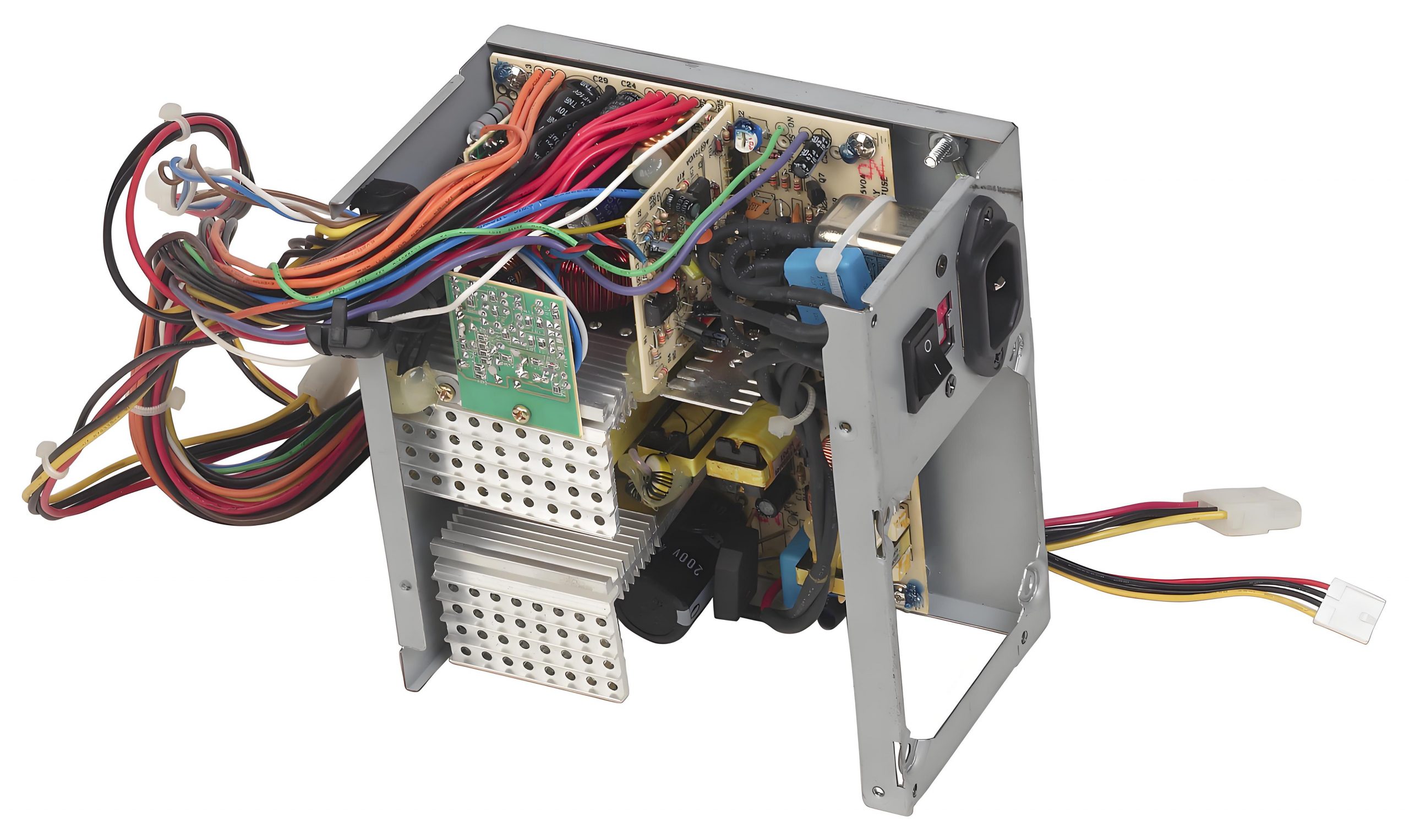
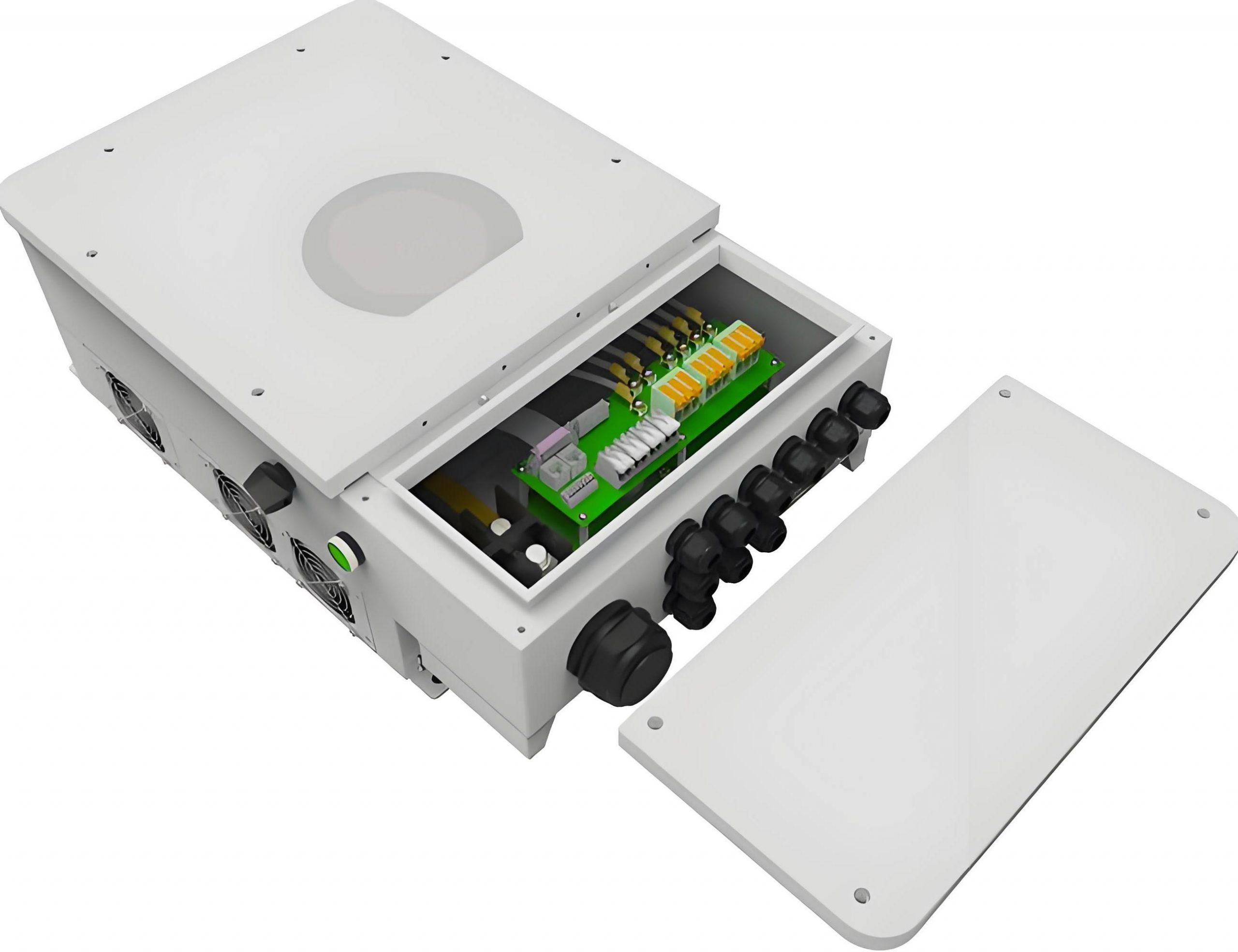
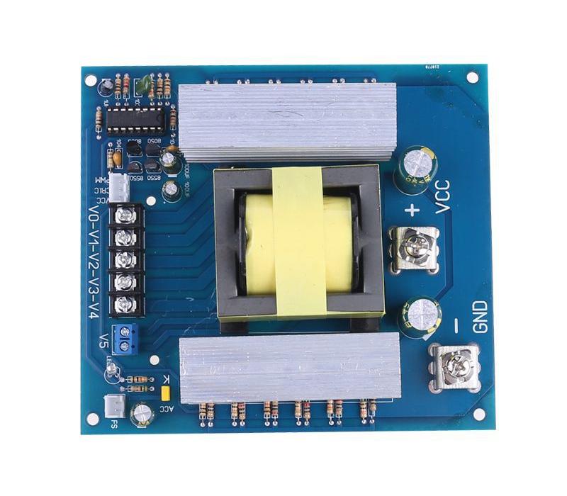
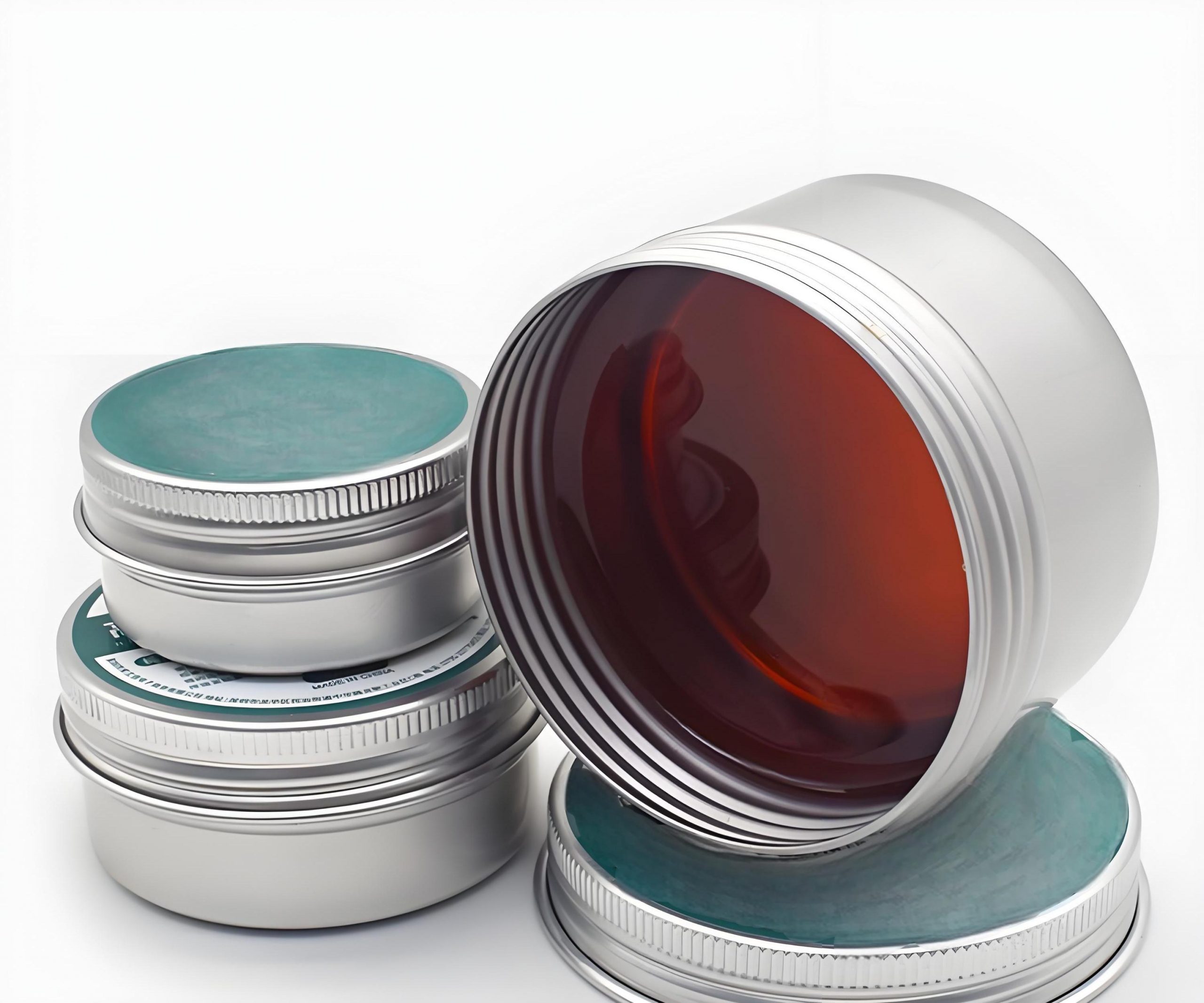
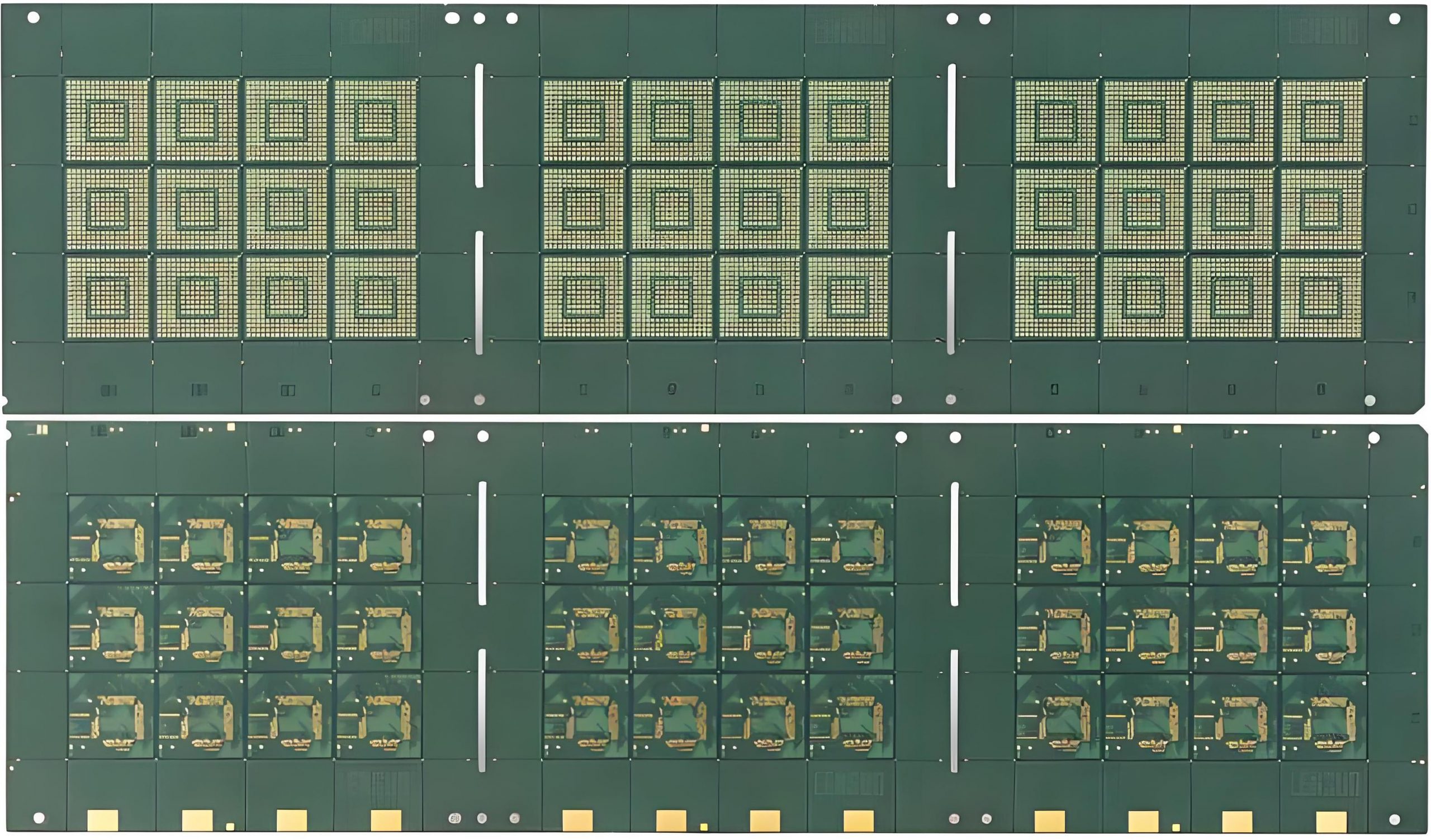
Photos of Solder Resist
While solder resist is typically green, variations exist depending on the design and function of the PCB. Photosensitive solder resist, for example, is often used in more intricate PCB designs because it allows for precise control of where the resist material is applied. Below are some examples of PCBs showcasing different types of solder resist and their impact on the circuit layout.
What Does Solder Resist Do?
Solder resist plays several critical roles in PCB manufacturing:
1. Prevents Short Circuits
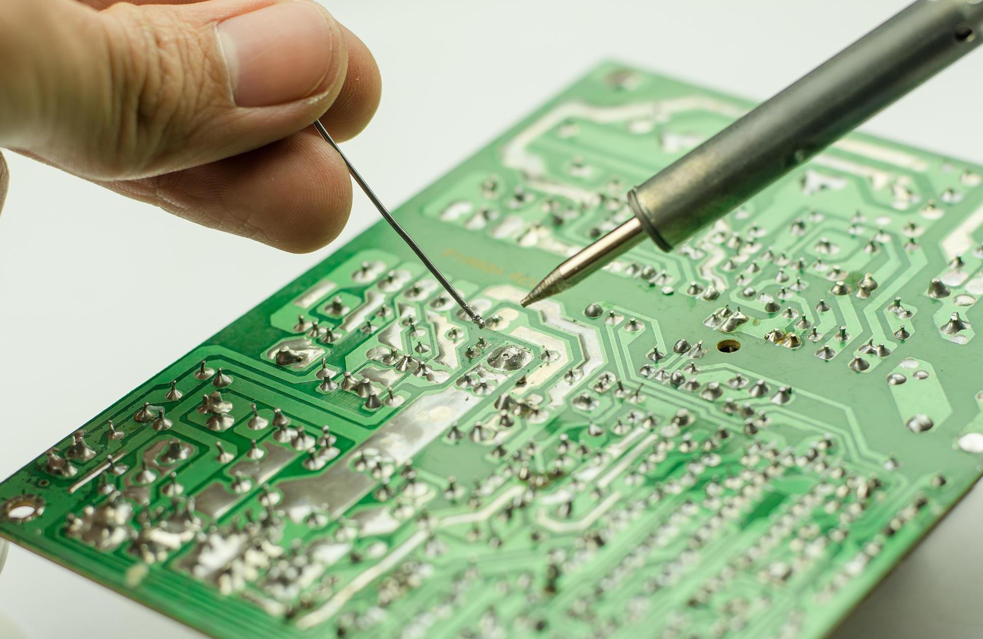
One of the key roles of solder resist is to prevent solder from adhering to areas other than the intended electrical contacts on a printed circuit board (PCB). During the soldering process, it ensures that solder only sticks to the pads where components are placed. By blocking solder from unwanted areas, it ensures that electrical connections are not unintentionally bridged.
2. Protecting Circuit Patterns from Dust, Heat, and Moisture
Solder resist acts as a protective shield, safeguarding the delicate circuit patterns from external factors like dust, heat, and moisture. These environmental conditions can otherwise compromise the performance and longevity of the PCB.
3. Supports Manufacturing / Smooth Manufacturing Process
A layer of solder resist guides the soldering process by clearly defining where the solder should go, smooth the whole process, making the entire assembly process more efficient.
4. Maintaining Electrical Insulation Between Circuit Patterns
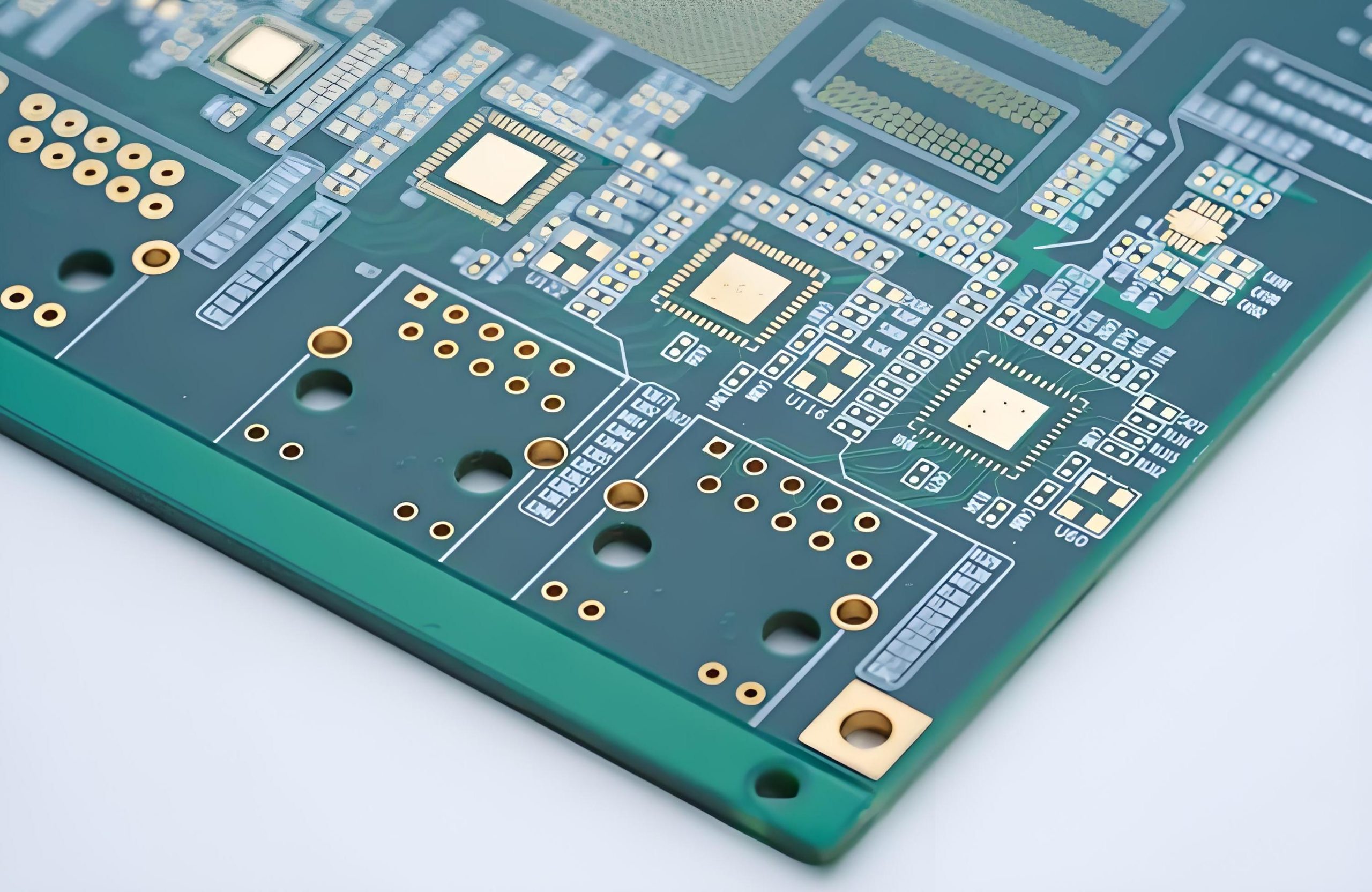
As electronic devices become smaller and more complex, the circuit patterns on PCBs have shrunk significantly, 50 to 150 µm dimensions are always commonly used in the market. And even thinner on advanced package boards. Solder resist ensures that these circuit patterns remain electrically insulated from one another, preventing accidental short circuits.
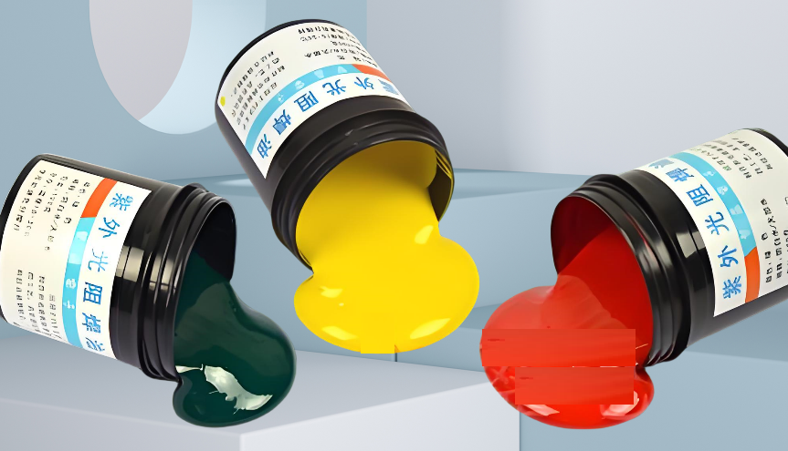
Solder Resist Material
Solder resist materials vary based on the requirements of the PCB and the intended application. The most common materials used include:
- Epoxy-based resists: These are widely used due to their excellent adhesion and resistance to high temperatures and chemicals.
- Acrylic-based resists: Known for their fast curing times and easier handling, they are suitable for mass production.
- Polyimide-based resists: Used for high-performance applications, especially in extreme environments.
The material selected depends on factors such as the desired performance, operating environment, and manufacturing capabilities. Each material has its advantages and is chosen according to the specific requirements of the PCB design.
What is the Thickness of Solder Resist?
The thickness of solder resist plays an important role in the overall performance of the PCB. Typically, the solder resist layer has a thickness between 15 and 30 microns (0.5mil to 1.2mil). The solder mask tends to be thinner near the edges of the traces and can be as thin as 0.3 mils or even less.
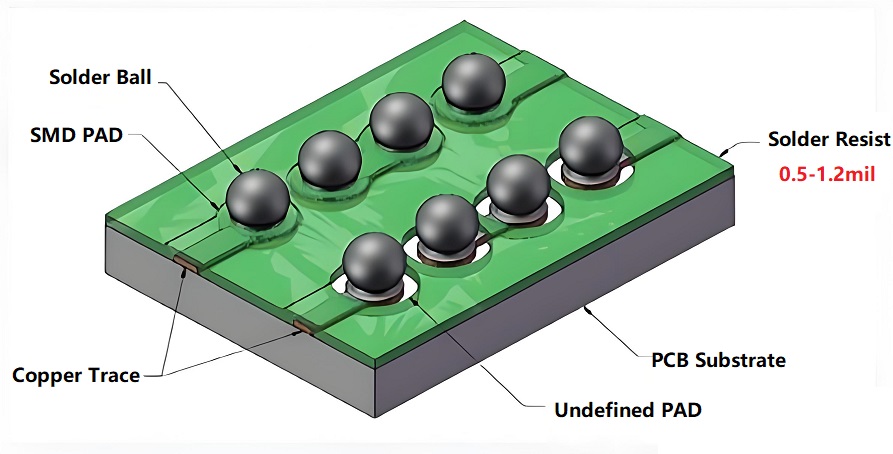
Typically, it’s recommended to have around 0.5 mils of solder mask covering the traces. This thickness ensures optimal protection without interfering with the soldering process or compromising the performance of the circuit. The exact thickness may vary depending on the complexity of the PCB design, but in general, it is thick enough to protect the copper traces while being thin enough to not interfere with the components’ performance. If you can’t make a decision about the solder resist thickness, it is a good way to ask a trust PCB manufacturer to get your answer, such as EBest Circuit (Best Technology).
Solder Resist vs. Solder Mask
Many people are confused about solder mask and solder resist: “Are they same or what are the differences between them?”
Actually, the terms solder resist and solder mask are essentially referring to the same concept. Both terms describe the protective layer applied to PCBs to prevent solder from bridging unwanted areas. While “solder mask” is commonly used, “solder resist” is more technically accurate since the resist material resists the solder during the assembly process. However, both terms are widely interchangeable in the industry.
Solder Resist Colors
While green is the most widely recognized color for solder resist, it’s far from the only option available. Solder resist can be found in a variety of colors, including red, blue, black, yellow, and even white, depending on the requirements of the PCB design or the specific application where this PCB will be used. These color variations serve different purposes, ranging from aesthetic preferences to functional considerations.
For example, some high-end or custom-designed PCBs may use colors like black or blue to create a distinct visual identity or to align with branding guidelines. In industries like aerospace or medical devices, where high-performance and unique design are often crucial, color may also be chosen for its visibility during the manufacturing process or in final product assembly.
However, the color choice isn’t only about appearance. In some cases, it can help with thermal conductivity, which can be important for applications that involve high-power circuits. Additionally, certain colors are more reflective under UV light, which aids in the photolithographic process. For example, blue solder resist can be beneficial for high-resolution applications, as it tends to make the ultraviolet light exposure process more precise. We’ve introduced the detailed functions about PCB colors in our other blogs:
- Why Choose Blue Circuit Board? Blue PCB vs Green Circuit Board?
- Unlock the Full Power of Circuit Board White
- Why Are Circuit Board Black Becoming Increasingly Popular?
- Uncover The Benefits And Applications Of Circuit Board Red
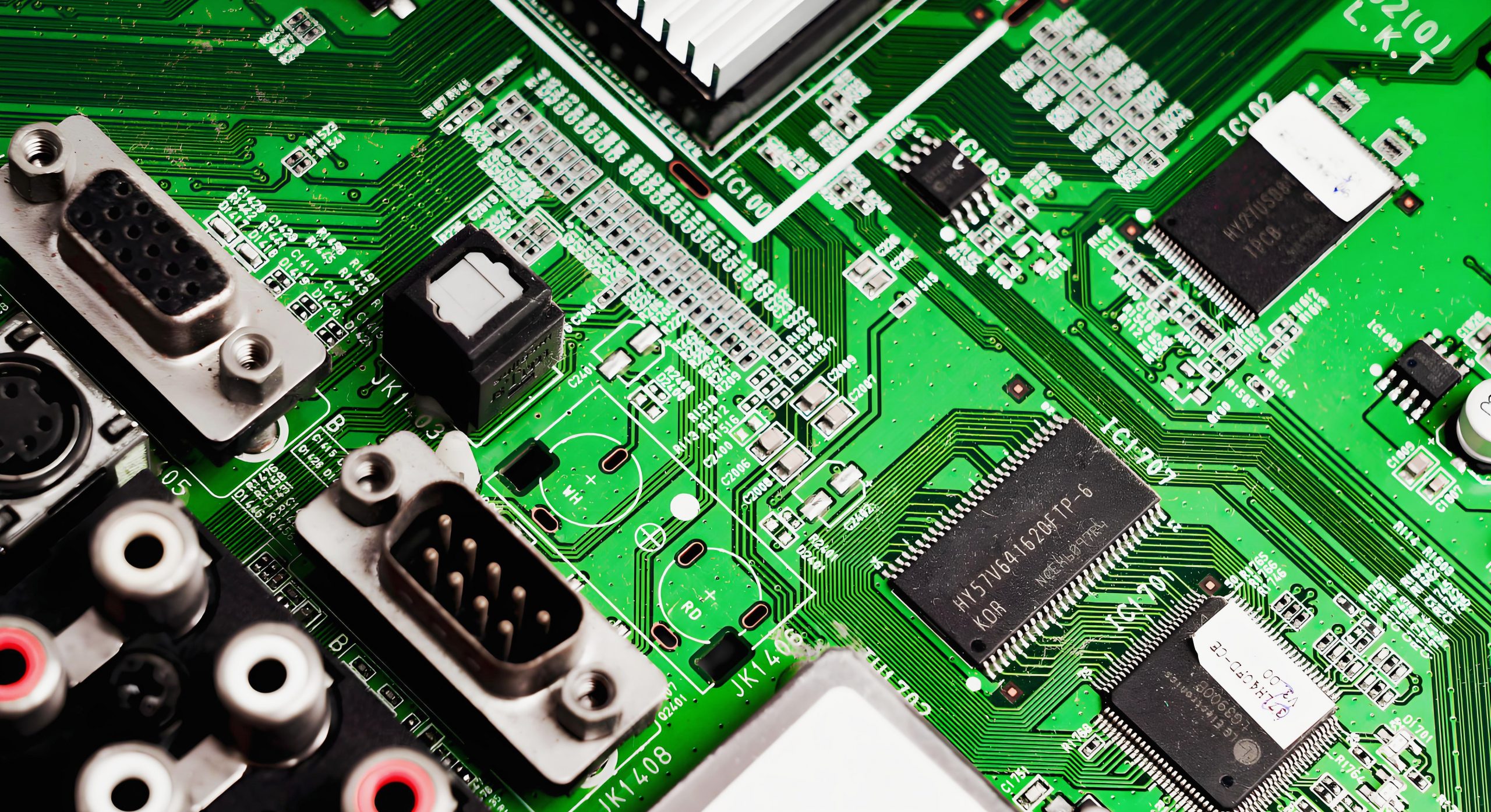
Why is Solder Resist Green?
While various colors of solder resist exist, green has become the industry standard for a variety of reasons, many of which are practical rather than just aesthetic.
- High Contrast and Visibility
One of the main reasons for the green color’s dominance is its high visibility, especially under ultraviolet (UV) light. During the PCB manufacturing process, photolithography is used to expose specific areas of the board to UV light. Green solder resist is highly visible under UV, so FQC (final quality check) inspectors can inspect the board for defects or imperfections in the soldering process.
- Optimal Performance in Photolithography
The process of applying solder resist involves exposing the board to UV light, which causes the resist material to harden in specific patterns. Green solder resist material is particularly well-suited to this process, as it is engineered to react efficiently to UV exposure.
- Cost-Effectiveness and Standardization
Another reason green solder resist is so commonly used is its cost-effectiveness. Green has become the default color because it is the most widely produced, and cost effective. Standardizing on green also simplifies production processes, as manufacturers can keep a consistent stock of the same type of material.
- Historical Tradition
The history of green solder resist dates back to the early days of PCB manufacturing. Green was originally chosen due to its availability, as it was one of the first colors of solder resist to be mass-produced. Over time, this color became synonymous with PCBs, and manufacturers continued to use it because it had already proven reliable and effective.
- Visual Appeal
Finally, there’s a practical and visual appeal to the green color. Green provides a clean, professional look for most PCBs and offers a neutral backdrop that allows the components and circuitry to stand out clearly. This is important, especially for high-precision and high-performance boards that need to be easily inspected for quality.
At EBest Circuit (Best Technology), we pride ourselves on over 18 years of expertise in the PCB manufacturing industry. As a trusted leader, we specialize in providing high-quality, reliable PCBs tailored to meet the specific needs of a wide range of industries, including automotive, telecommunications, and consumer electronics. Our expertise in solder resist application plays a vital role in maintaining the integrity of your circuits and preventing soldering issues while enhancing the overall lifespan of your PCBs. Meanwhile, we offer various color of solder resist, whatever you want, we can make it into reality. Contact us and get your own customized PCB now!