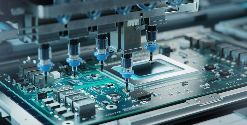
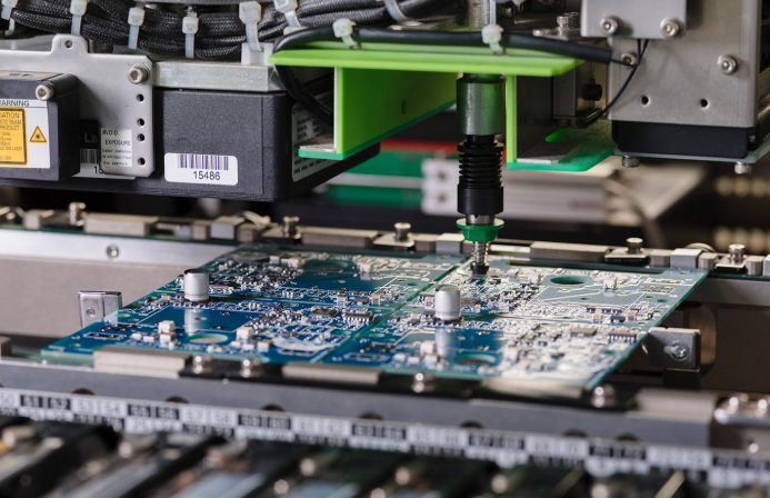
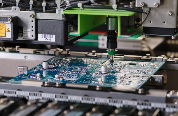
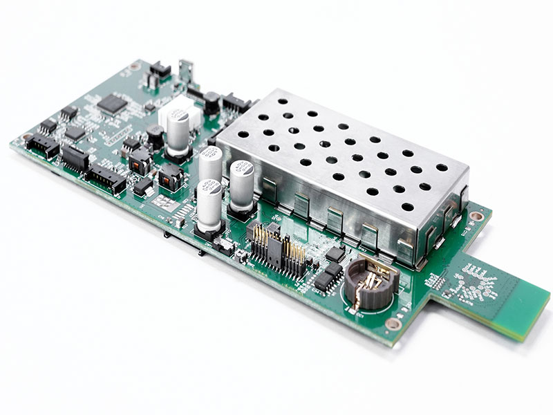
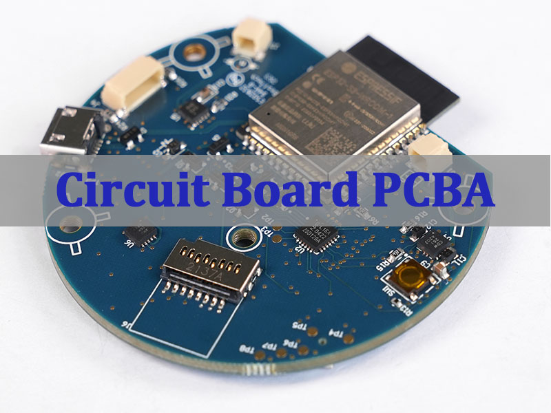
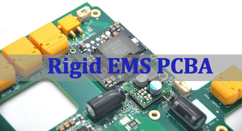
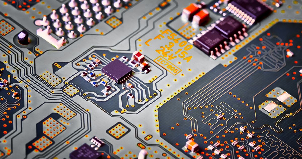
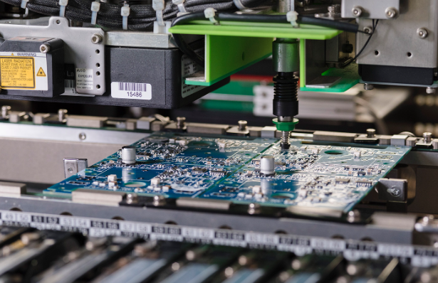
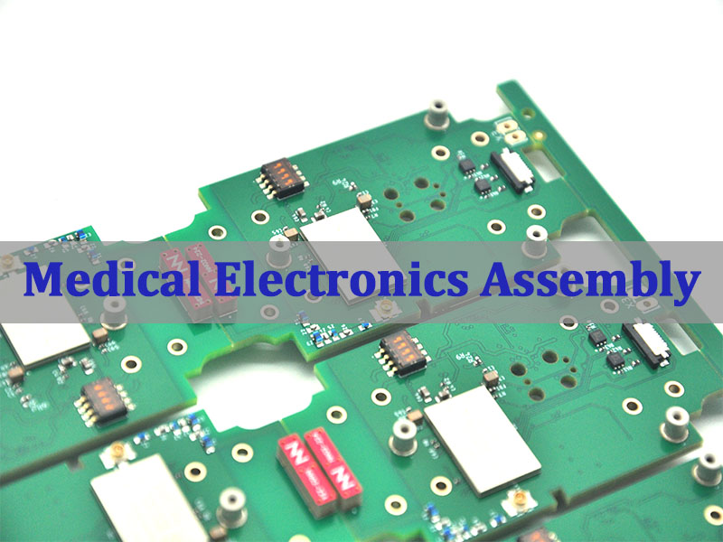
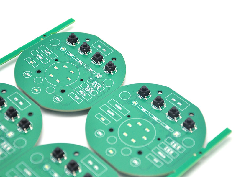
Medical electronics assembly refers to the specialized assembly of electronic circuits used in regulated medical devices, where reliability, traceability, and compliance are mandatory rather than optional.
In real manufacturing practice, medical electronics assembly directly impacts patient safety, device accuracy, and long-term regulatory acceptance.
This article explains how medical electronics assembly is executed, how compliance and quality risks are controlled, and how to evaluate suppliers for both prototype and volume production. EBest Circuit (Best Technology) provides medical electronics assembly services for regulated applications. For project inquiries or orders, please contact us via sales@bestpcbs.com.
What Is Medical Electronics Assembly and Why Is It Critical?
Medical electronics assembly is a form of medical device electronics assembly designed for products that operate under strict regulatory oversight.
Unlike consumer electronics, assembling electronic medical devices requires validated processes and documented controls.
Typical applications include:
- Patient monitoring and diagnostic systems
- Imaging and sensing equipment
- Therapeutic and life-support devices
In these products, even minor assembly variation can lead to functional drift or compliance failure.
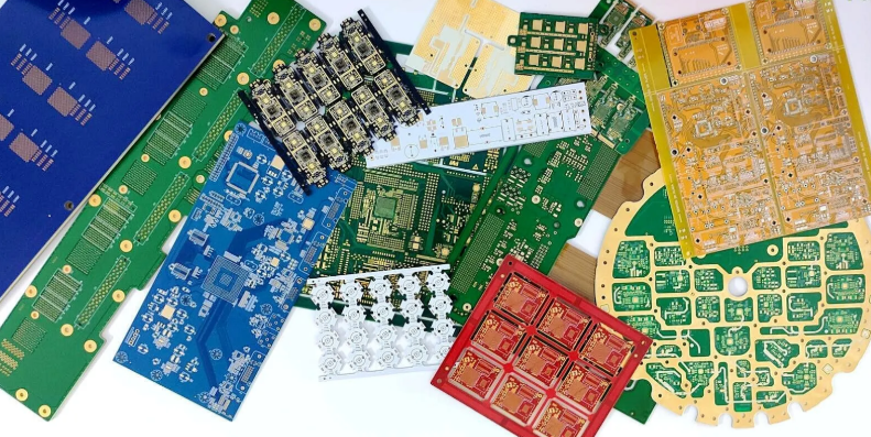
How Medical Electronics Assembly Differs from Standard PCBA?
Medical electronics assembly is fundamentally different from general-purpose PCBA.
The difference lies not in component type, but in process discipline and documentation depth.
Key differences include:
- Mandatory traceability at material and batch level
- Tighter process windows and change control
- Audit-ready records for every build
This is why medical electronic assembly suppliers cannot be evaluated using consumer PCBA criteria.
Which Medical Devices Require Electronics Assembly?
Nearly all modern medical devices rely on electronic assemblies for sensing, control, and communication.
Assembling electronic medical devices requires alignment between design intent and manufacturing reality.
Common categories include:
- Portable diagnostic instruments
- Wearable and monitoring devices
- Control electronics for therapeutic systems
Each category carries different risk levels, but all require controlled assembly environments.
What Certifications Are Required for Medical Electronics Assembly?
Certification defines whether a supplier is eligible for regulated projects.
Medical electronics assembly certification is often a gating requirement during supplier qualification.
Commonly required certifications include:
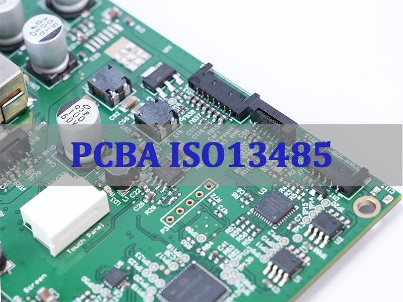
- ISO 13485 for medical quality management
- ISO 9001 for manufacturing consistency
- IATF 16949 / AS9100D for high-reliability systems
However, certification value depends on how deeply it is implemented in daily operations.
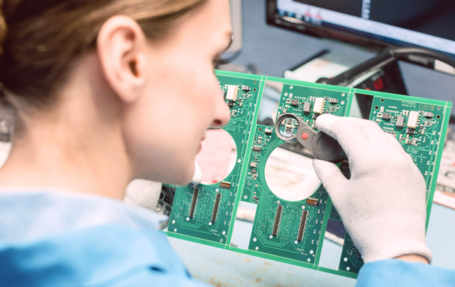
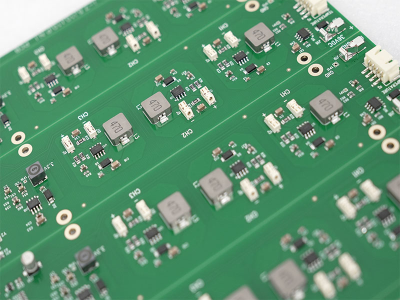
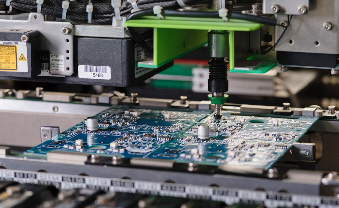
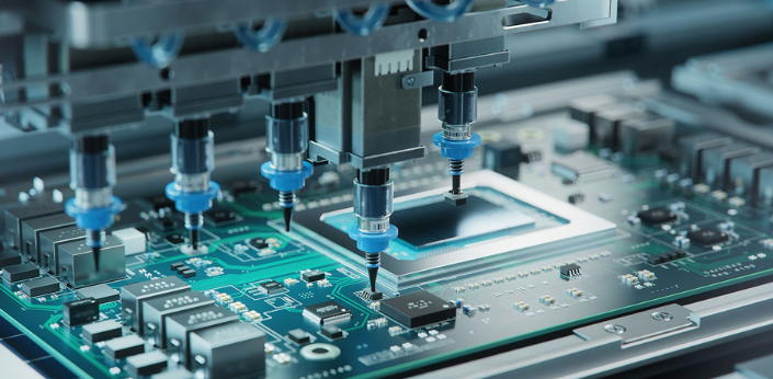
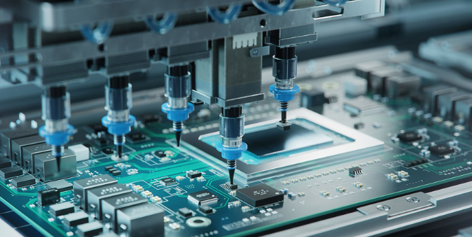
Key Quality Control Requirements in Medical Electronics Assembly
Quality control in medical electronics focuses on prevention rather than post-assembly detection.
Process stability is more important than inspection volume.
Core controls include:
- Incoming material verification and lot control
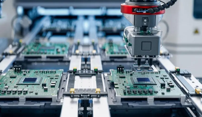
- Process parameter locking across SMT lines
- AOI, functional testing, and controlled rework
These controls ensure repeatability across product lifecycle stages.
DFM and Engineering Review for Medical Device Electronics
DFM review is not optional in medical device electronics assembly.
It is the primary mechanism for preventing latent defects and regulatory risk.
A structured DFM review typically includes:
- Footprint and solderability analysis
- BOM risk assessment and optimization
- Process compatibility verification
Early DFM intervention significantly reduces downstream corrective actions.
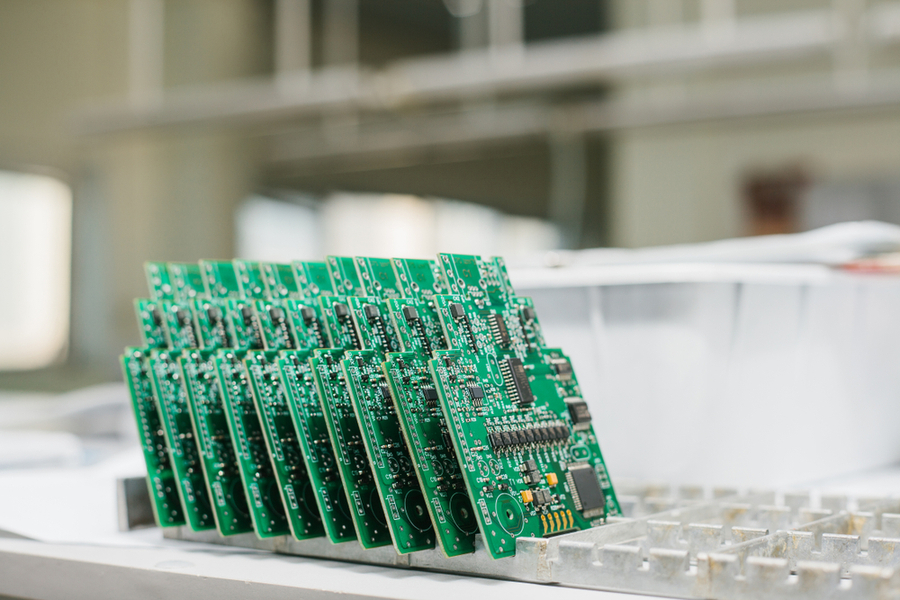
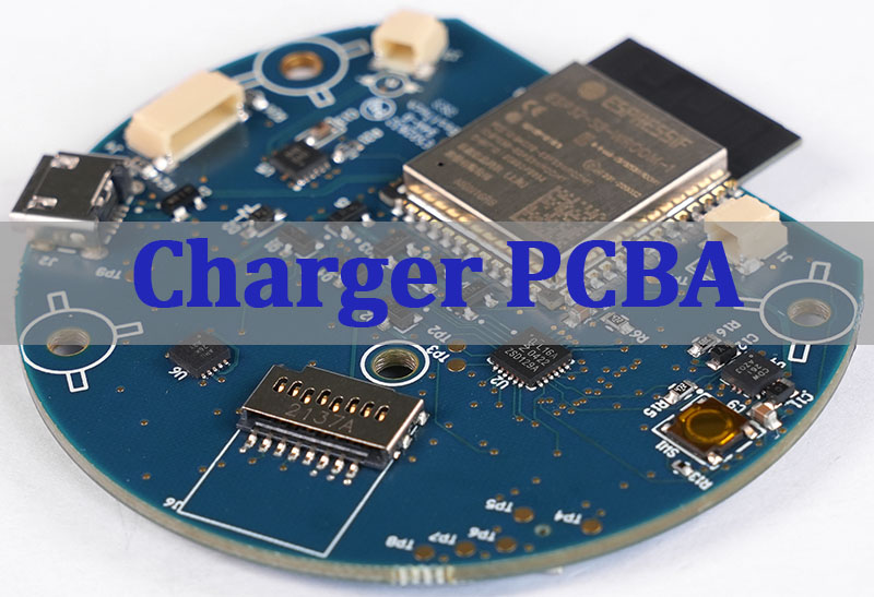
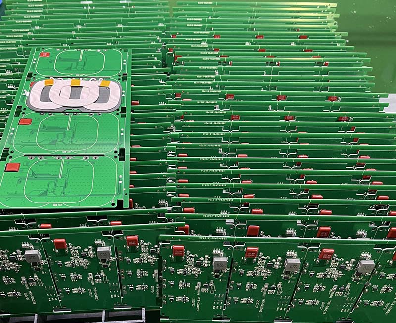
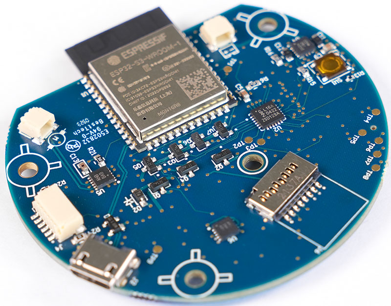
Prototype vs Volume Medical Electronics Assembly
Prototype medical assembly emphasizes validation and design verification.
Volume production emphasizes consistency, traceability, and audit readiness.
Key distinctions:
- Prototype builds allow controlled flexibility
- Volume builds require frozen processes and formal change approval
Using the same supplier across both phases reduces transfer and requalification risk.
Traceability and Documentation in Medical Electronics Assembly
Traceability is a non-negotiable requirement in medical electronics.
It enables fast root-cause analysis and regulatory reporting.
Typical traceability scope includes:
- Material lot and component batch tracking
- Assembly and test records per production batch
- Process deviation and corrective action logs
This level of documentation differentiates compliant suppliers from generic assemblers.
Medical Electronics Assembly in China: Risk and Control
Medical electronics assembly China is widely adopted when supported by proper controls and audits.
Geography is not the risk factor; process discipline is.
Reliable suppliers provide:
- Transparent documentation access
- Stable production lines
- Cooperative audit support
Pilot builds and validation runs are standard risk-mitigation steps.
How Much Does Medical Electronics Assembly Cost?
Medical electronics assembly costs are higher than standard PCBA due to additional controls and documentation.
Pricing reflects risk management rather than component placement alone.
Typical reference ranges (excluding components):
- Prototype: USD 15–40 per board
- Small batch: USD 10–25 per board
- Volume production: USD 6–15 per board
Actual cost depends on test depth, traceability scope, and process validation level.
How to Choose a Reliable Medical Electronics Assembly Partner
Selecting a medical electronics assembly partner is a risk-management decision.
Engineering depth matters more than advertised capacity.
Evaluation criteria include:
- Active medical certifications
- DFM and validation capability
- Documentation discipline
- Long-term process stability
This approach reduces lifecycle and regulatory exposure.
In closing, this article outlined how medical electronics assembly is performed under regulated manufacturing requirements, how quality and compliance risks are controlled, and how to select a qualified partner for prototype and volume production.
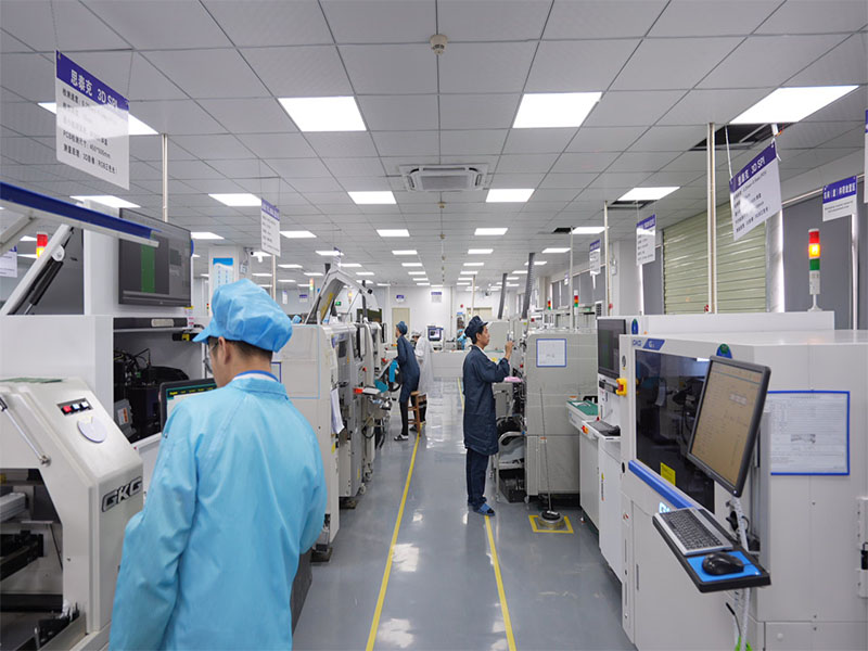
EBest Circuit (Best Technology) supports medical electronics assembly through DFM pre-review, BOM optimization, and hands-on engineering guidance provided by PCB and PCBA specialists with over 20 years of experience in medical device projects. Our integrated service model supports prototypes, small batches, and fast PCBA delivery in as little as 1.5 weeks, enabling engineering teams to validate designs efficiently and transition smoothly into production. If you are planning a medical electronics assembly project or require technical consultation, please feel free to contact sales@bestpcbs.com.
FAQ: Medical Electronics Assembly Questions
Q1: Is ISO 13485 mandatory for medical electronics assembly?
Yes, for most regulated medical devices.
Q2: Can medical electronics be prototyped quickly?
Yes, with validated processes and controlled documentation.
Q3: How is traceability implemented?
Through material lot tracking and batch-level production records.
Q4: Is China suitable for medical electronics assembly?
Yes, when supported by audits and validated process controls.
Q5: How long does medical electronics assembly take?
Prototypes typically take 1–2 weeks; production takes 3–6 weeks.