The "Thick Film" refers to the thickness of conductor layer on Ceramic PCB. Normally the thickness will be at least exceeds 10 miron (um), around 10~13um, more thick than spurting technology in Thin Film Ceramic PCB. Of course thickness is less than
DCB Ceramic board or
FR4 board.
At the same time, using thick film technology, we can put resistor, electric capacity, conductor, semi-conductor, and interchangable conductor on ceramic board, after manufacturing steps of printing and high temperature sintering. We can make all the resistors with the same value, or different value for different resistor on the same board.
Basic Parameter of Thick Film Ceramic Board
Substrate can be 96% or 98% Alumina (Al2O3) or Beryllium Oxide (BeO), thickness range: 0.25, 0.38, 0.50mm, 0.635mm (default thickness), 0.76mm, 1.0mm. Thicker thickness such as 1.6mm or 2.0mm can be customized too.
Conductor layer materail is silver palladium, gold palladium, or Mo/Mu+Ni (for Ozone);
Thickness of conductor >= 10 miron (um), and Max can be 20 micron (0.02mm)
Min trace width and space for volume production:0.30mm & 0.30mm, 0.20mm/0.20mm is also okay but cost will be higher, and 0.15mm/0.20mm only available for prototype.
Tolerance for final trace layout will be +/-10%
Both gold and silver palladium is workable for gold-wire bonding, but customer need to mention that so that we will use special silver palladium which is suitable for that artwork.
Gold palladium is much more expensive than silver, about 10~20 times higher
More different resistor value on the same board, more expensive board will be
Normally layers are 1L and 2L (with plated through hole (PTH), and plated material is the same like the one used for conductor), and maximum layers can be 10 layers
Only board with Rectrangle shape can be shipped via single piece, or via panel
Soldermask is also available upon request, working temperature >500 C, and color is semi-transparent
For same stack up, cost lower than DCB, higher than MCPCB
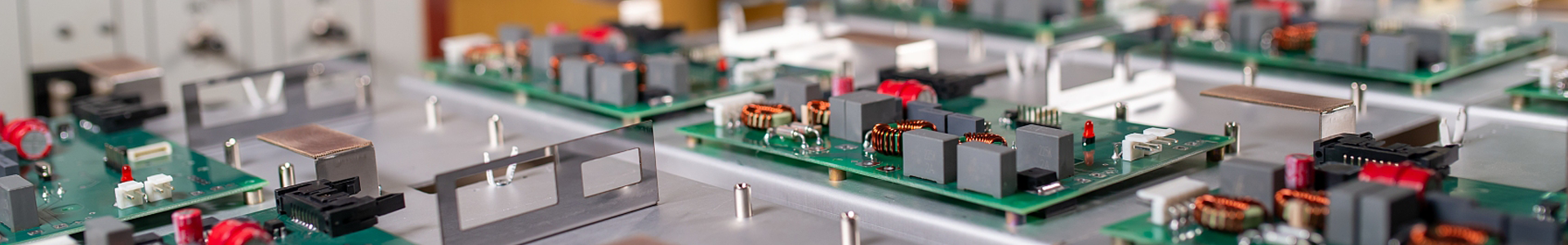
Application of Thick Film Ceramic PCB
High-power LED
Chip, Wafter
Street light, High bright light
Automotive light system
Hybrid integrated circuit for automotive
Fuel Sendor Resistor Card
Injection System
Anti-block Braking system
High-power electronic semi-conductor module
electric power transmitter modules
Semiconductor process equipment
Solar cell
Sensor
Telecome device
Please click here for immediate quotation online Please contact us today for more information about Thick Film Ceramic circuit board.