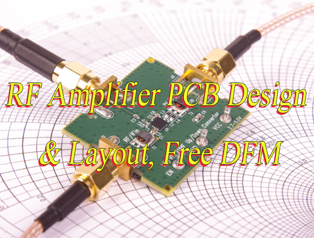
How can an RF microwave PCB keep high-frequency signals stable when small design and fabrication changes may affect the final result? This guide explains how RF microwave PCB boards work, how to choose suitable materials, how to control impedance and signal loss, and how to select the right manufacturer for prototype and production projects.
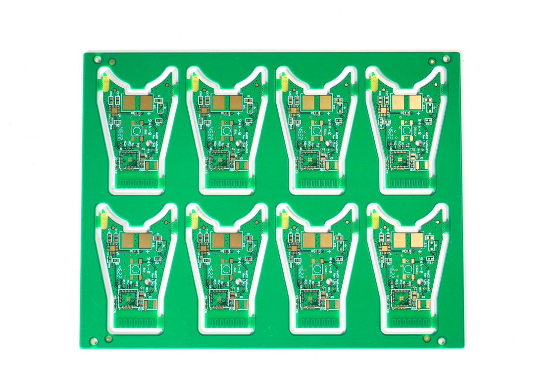
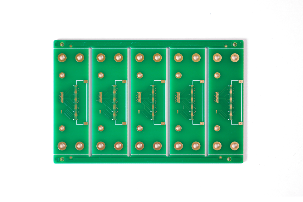
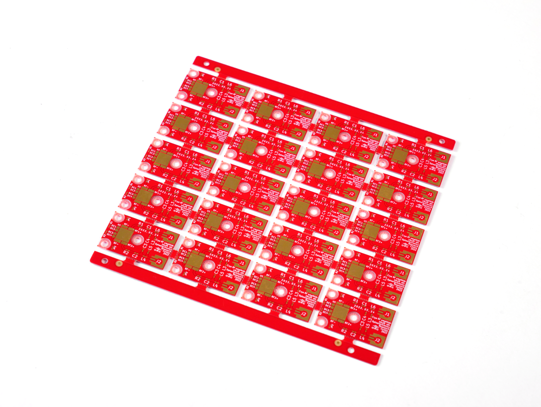
EBest Circuit (Best Technology) is an engineering-driven PCB and PCBA manufacturer with over 20 years of experience supporting high-frequency, RF, microwave, automotive, medical, industrial, communication, and aerospace/UAV projects. With self-owned PCB and PCBA factories, EBest provides DFM review, material selection support, controlled impedance PCB fabrication, component sourcing, assembly, testing, and production-quality support from prototype to mass production.
If you are evaluating an RF microwave PCB project and need practical manufacturing feedback, you can send your Gerber files, stackup, material requirements, and quantity to sales@bestpcbs.com for a technical review and quotation.
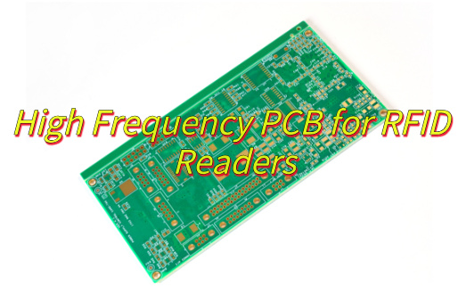
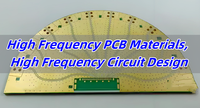
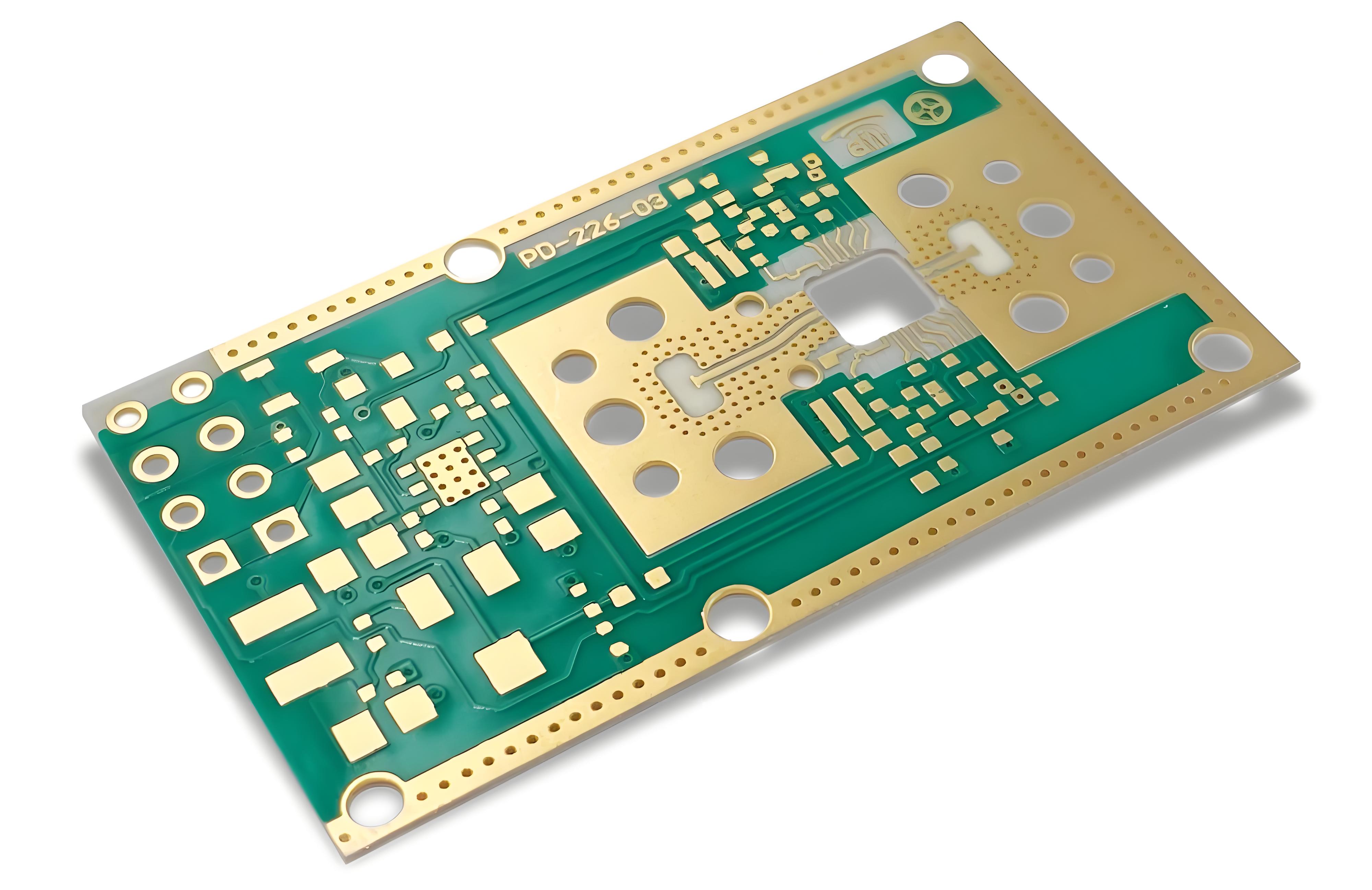
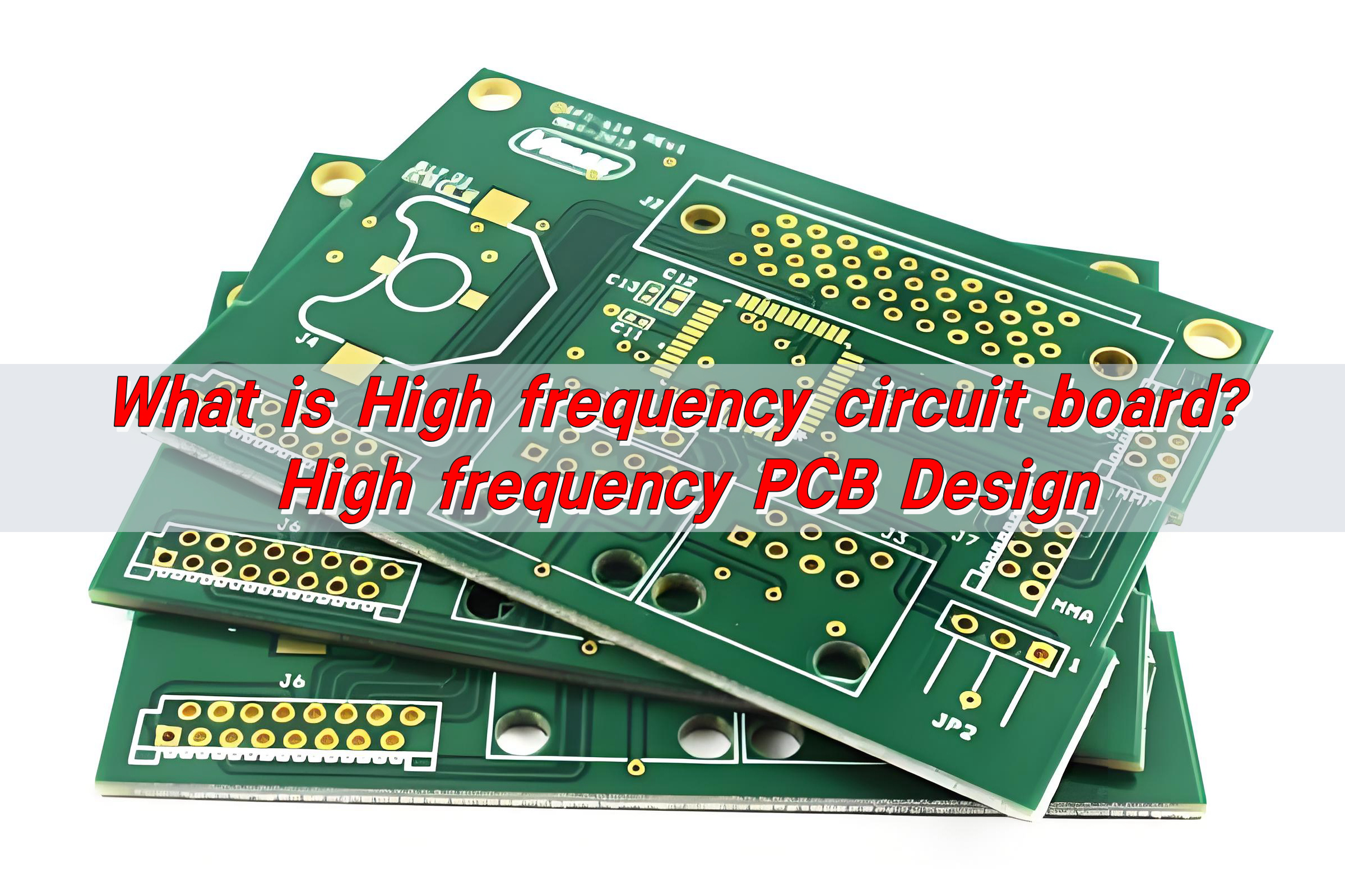
What Is an RF Microwave PCB Board?
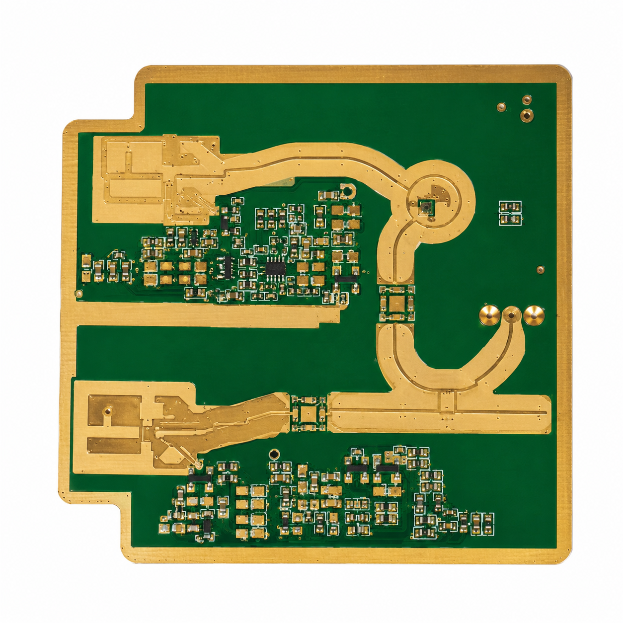
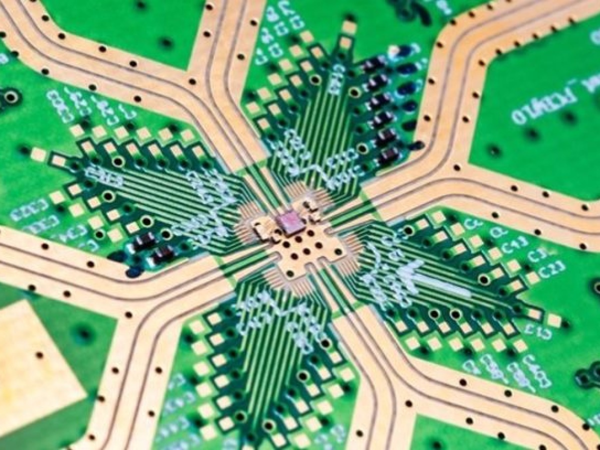
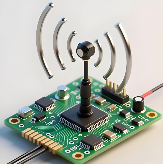
An RF microwave PCB board is a printed circuit board made for radio frequency and microwave signals. It is a high-frequency circuit board designed for RF and microwave signal transmission, usually covering applications from MHz-level RF circuits to GHz and millimeter-wave systems.
In simple terms, RF board PCB is a broader category for radio-frequency circuits, microwave PCB usually refers to higher-frequency GHz-range circuits, and RF microwave PCB board is often used to describe a low-loss, impedance-controlled PCB built for both RF and microwave performance.
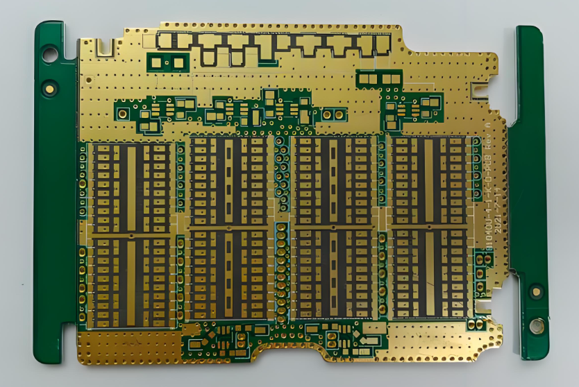
Unlike a standard FR4 PCB, an RF microwave PCB is part of the signal path. Therefore, the board does more than connect components. It also affects signal speed, loss, phase, reflection, and radiation.
In many low-speed PCB designs, small material changes may not create serious issues. However, RF and microwave circuits are more sensitive. A small shift in dielectric thickness, copper roughness, or trace width can change the final electrical behavior.
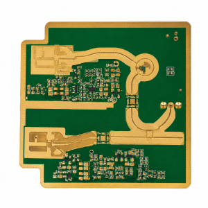
RF microwave PCB boards are commonly used in:
- 5G communication modules
- RF antennas
- Radar systems
- Satellite communication equipment
- Aerospace and UAV electronics
- Industrial RF systems
- Medical RF devices
- Automotive radar and sensing modules
- High-frequency test instruments

As a result, RF microwave PCB design must start with clear electrical goals. These goals may include low insertion loss, stable impedance, low return loss, strong grounding, and repeatable batch performance.
A well-built RF microwave PCB helps engineers reduce signal loss and improve circuit stability. It also makes the product easier to move from prototype to mass production.
How Does an RF Microwave High-Frequency PCB Work?
An RF microwave high-frequency PCB works by guiding electromagnetic energy through controlled signal paths. These paths may include microstrip lines, stripline traces, coplanar waveguides, grounded coplanar waveguides, and antenna feed lines.
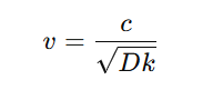
At high frequencies, a copper trace is not just a simple wire. Instead, it works as a transmission line. The signal travels through both the copper and the surrounding dielectric field. Because of this, the material, trace width, spacing, ground plane, and via structure all affect performance.
Several factors matter most.
- Impedance control is one of the first concerns. Many RF circuits use 50 ohm impedance, although some designs use other values. The final impedance depends on trace width, copper thickness, dielectric thickness, and dielectric constant.
- Insertion loss is also important. It shows how much signal power is lost as the signal moves through the board. Loss can come from the dielectric material, copper surface, radiation, and poor transitions.
- Return loss shows how much signal reflects back. Poor layout, sudden trace width changes, bad via design, or weak connector launch design may increase reflection.
- Phase stability matters in radar, antenna, and communication systems. If the material or process changes too much, phase behavior may shift. This can affect signal timing and accuracy.
- Ground return path is another key factor. RF current needs a clean return path. Therefore, a continuous ground plane and proper via stitching can help reduce noise, coupling, and radiation.
In short, an RF microwave PCB works well when the signal sees a stable path from the source to the load. Good design creates that path. Good fabrication keeps it consistent.
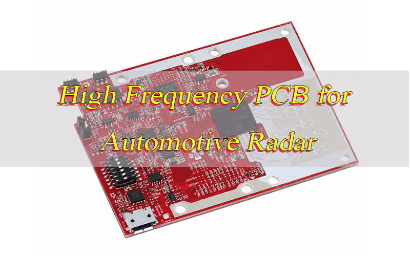
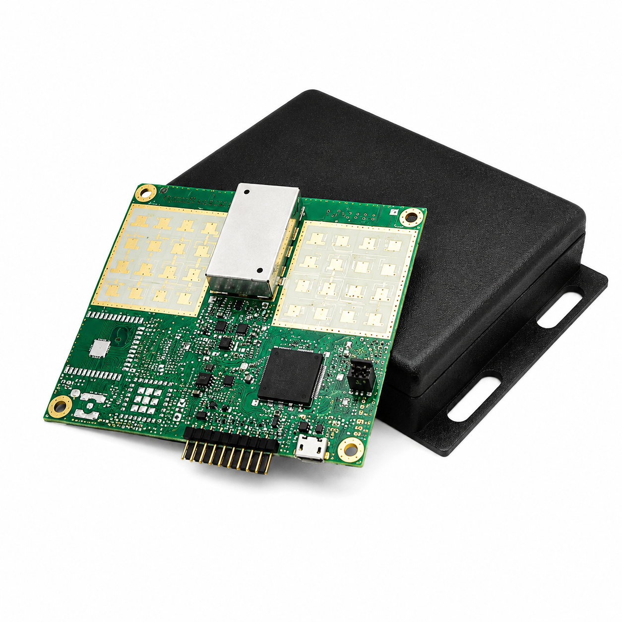
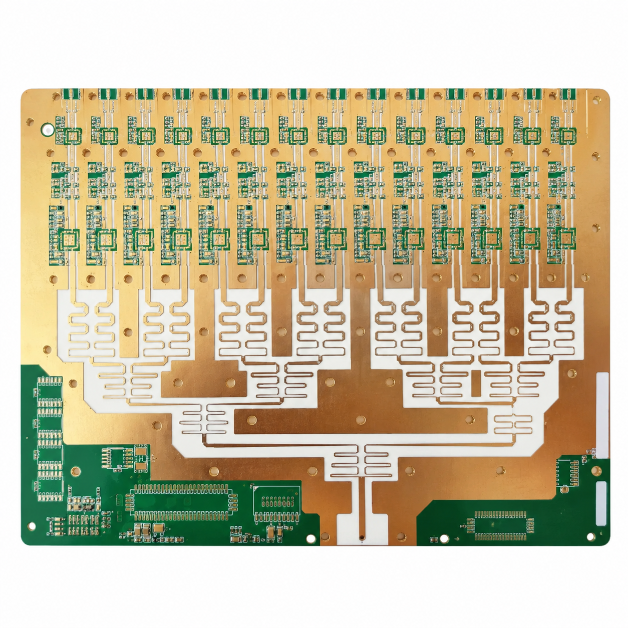
Where Are RF Microwave PCB Boards Used in 24GHz, 5G, and High-Power Applications?
RF microwave PCB boards are used in products where frequency, bandwidth, signal loss, and stability matter. Some boards are small antenna modules. Others are complex multilayer boards for communication systems.
| Application Area | Typical Requirement | PCB Focus |
|---|---|---|
| 24GHz radar | Stable detection and low signal drift | Low-loss laminate, precise impedance, antenna accuracy |
| 5G RF modules | High bandwidth and stable transfer | Stable Dk/Df, fine-line control, hybrid stackup |
| RF antennas | Good radiation efficiency | Antenna geometry, copper tolerance, surface finish |
| Base stations | Long-term signal reliability | Thermal control, material consistency, multilayer control |
| Aerospace and UAV | Lightweight and stable RF performance | Traceability, process control, vibration resistance |
| Industrial RF equipment | Reliable field operation | Strong structure, thermal reliability, test control |
| High-power RF modules | Heat control and signal stability | Metal-backed structure, thermal path, copper control |
- For a 24GHz RF microwave PCB, material choice and layout precision are already important. As the frequency rises, small geometry changes become more visible in actual RF performance.
- For 5G-ready RF microwave high-frequency PCB fabrication, engineers often need low transmission loss, stable dielectric properties, and repeatable production. In many cases, they also need hybrid stackups. These stackups combine RF materials with FR4 or other support layers.
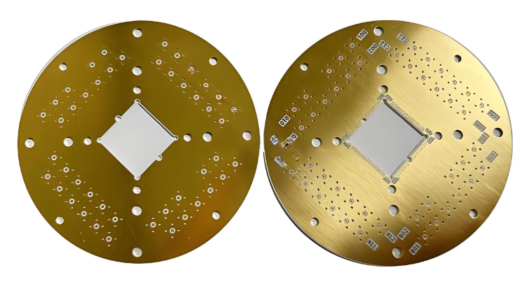
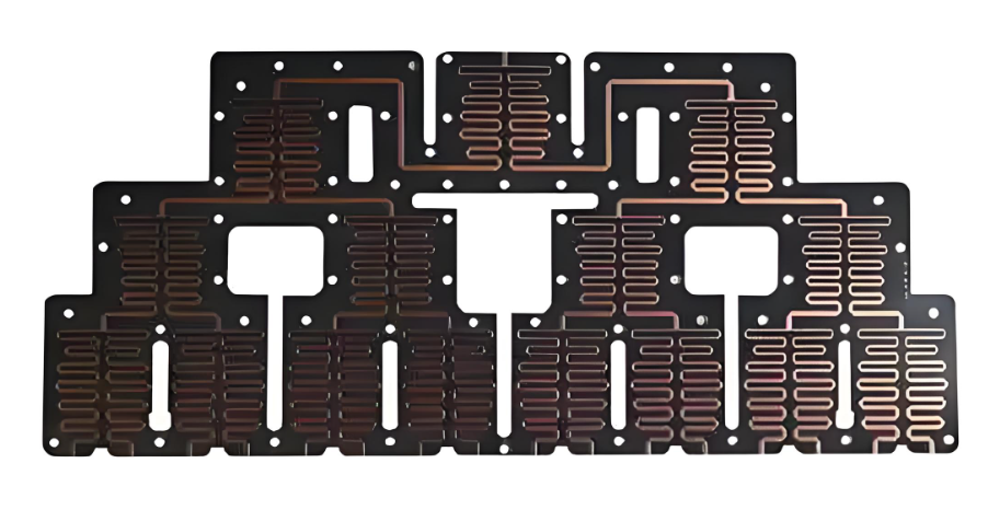
- Meanwhile, high-power RF applications add another challenge: heat. These boards may need metal-backed structures, thermal vias, heavy copper areas, or a dedicated heat path.
Therefore, the best RF microwave PCB is not always the most complex board. It is the board that fits the signal, thermal, mechanical, and production needs of the product.
How to Do PCB Material Selection for RF Microwave Millimeter-Wave Design?
Material selection is one of the most important steps in RF microwave PCB design. The laminate affects signal loss, impedance, phase stability, heat control, and long-term reliability.
For PCB material selection for RF microwave millimeter-wave design, engineers usually check several material properties.
| Material Factor | Why It Matters |
|---|---|
| Dielectric constant, Dk | Affects trace width, impedance, wavelength, and phase speed |
| Dissipation factor, Df | Affects dielectric loss, especially at high frequency |
| Copper roughness | Affects conductor loss and signal attenuation |
| Thermal conductivity | Helps move heat away from RF power areas |
| CTE | Affects dimensional stability and via reliability |
| Moisture absorption | Affects dielectric stability and long-term use |
| Process compatibility | Affects drilling, lamination, routing, and yield |
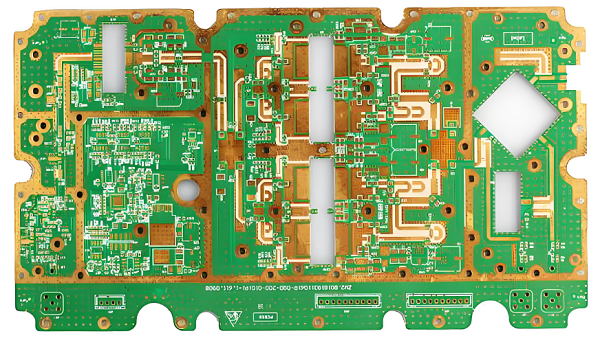
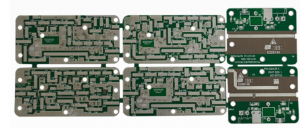
Common RF microwave PCB materials include Rogers high-frequency laminates, PTFE-based laminates, ceramic-filled hydrocarbon materials, Taconic materials, and other low-loss substrates.
However, the lowest-loss material is not always the best choice. The project may also need cost control, easy sourcing, stable production, and strong mechanical performance. Therefore, engineers should choose the material based on frequency, loss target, thermal need, stackup, volume, and budget.
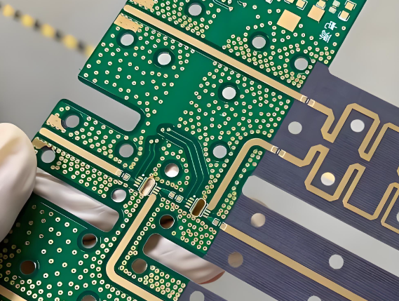
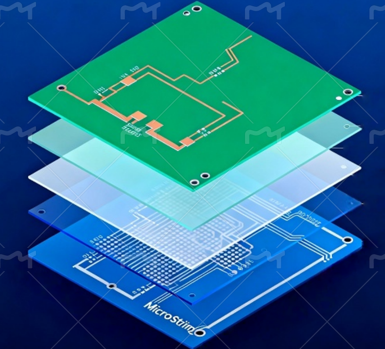
In some projects, a hybrid stackup is a practical choice. For example, the RF layer may use a low-loss material, while the support layers use FR4. This helps reduce cost while keeping the high-frequency path stable.
Before production, the material choice should be reviewed with the manufacturer. This can help avoid problems with drilling, lamination, copper control, and dimensional stability.
What Are the Main RF Microwave PCB Board Design and Layout Rules?
Good RF microwave PCB board design and layout starts with a clean signal path. The layout should reduce loss, avoid sudden impedance changes, and give RF signals a stable return path.
Here are the main design rules.
Keep RF traces short and direct.
- Shorter traces reduce loss and lower the risk of unwanted coupling. Also, avoid unnecessary stubs, long detours, and sharp changes in direction.
Control impedance from the start.
- The stackup, copper thickness, dielectric thickness, and trace width should be planned before layout. This helps avoid later redesign.
Use a continuous ground plane.
- A broken ground plane can disturb the return path. As a result, it may increase radiation and impedance mismatch.
Add ground via stitching where needed.
- Ground vias near RF traces can help control the electromagnetic field. They can also reduce coupling between nearby circuits.
Pay attention to via transitions.
- At high frequency, a via can create unwanted inductance and capacitance. Therefore, via size, pad size, anti-pad size, and via depth should be reviewed.
Separate noisy circuits from RF areas.
- Power converters, digital clocks, and fast switching signals should stay away from sensitive RF paths. In addition, proper shielding and layer planning can reduce noise.
Review solder mask over RF traces.
- Solder mask can change impedance because it adds material above the copper. Some RF designs need solder mask clearance over controlled traces.
Design connector launches carefully.
- A poor RF connector launch can create reflection and loss. Therefore, the launch area should match the connector type, stackup, and target impedance.
Overall, RF layout is not only about routing traces. It is about building a stable electrical environment around each signal path.
What Pain Points Come With RF Microwave PCB, and How Does EBest Solve Them?
RF microwave PCB projects often face issues that are not obvious at first. A board may look correct, but still fail RF testing. Therefore, early review and stable fabrication control are important.
| Customer Challenge | What Usually Happens | How EBest Supports the Project |
|---|---|---|
| Material choice is unclear | The customer knows the frequency, but not the best laminate | EBest reviews frequency, Dk/Df, stackup, heat, cost, and production volume before giving material suggestions |
| Impedance is hard to control | Small trace or dielectric changes may cause reflection | EBest supports controlled impedance fabrication and checks stackup, trace width, copper thickness, and impedance targets before production |
| Prototype results are hard to repeat | The first sample may work, but later batches may shift | EBest helps control material batches, etching, lamination, inspection, and process records |
| Hybrid stackups create process risk | RF material and FR4 may behave differently during lamination | EBest reviews hybrid stackup feasibility and gives DFM suggestions before fabrication |
| RF designs need PCB and assembly support | Customers may need bare boards, components, assembly, and testing | EBest provides PCB fabrication, component sourcing, PCBA assembly, and testing support under one workflow |
| Design files are not production-ready | Small layout issues may lead to delay or rework | EBest provides DFM pre-review to help customers find risks before the board enters production |
This structure keeps the problem and solution clear. It also helps buyers quickly see whether the manufacturer can support real project risks.
For RF microwave PCB projects, EBest does not only build boards from files. Instead, the engineering team can help review the practical manufacturing side of the design. This includes material selection, stackup, impedance control, trace tolerance, via design, and assembly needs.
As a result, customers can reduce trial-and-error during prototyping. They can also move more smoothly from sample builds to volume production.
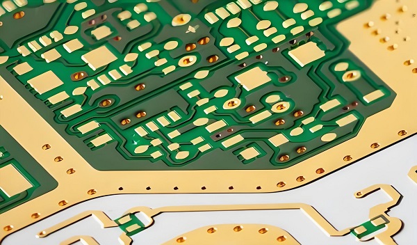
How Does RF Microwave PCB Fabrication Control Impedance, Loss, and Tolerance?
RF microwave PCB fabrication requires stable process control. The goal is to keep the finished board close to the original electrical design.
Several fabrication steps affect RF performance.
Material handling
- High-frequency materials may need special storage, drilling, lamination, and routing control. Good handling helps keep the material stable.
Stackup control
- Dielectric thickness affects impedance. Therefore, prepreg flow, lamination pressure, and material selection must stay consistent.
Etching control
- Trace width affects impedance and signal loss. The manufacturer must understand copper thickness and etching behavior. Then, it can apply proper compensation.
Copper thickness control
- Uneven copper can change impedance. It can also affect conductor loss. Stable plating helps improve consistency.
Drilling and via quality
- Vias affect RF transitions and board reliability. Clean drilling, proper desmear, and stable copper plating are important.
Surface finish selection
- ENIG, immersion silver, OSP, and other finishes may affect solderability and surface behavior. The right finish depends on RF needs, assembly process, storage time, and customer standards.
Impedance testing
- TDR testing and impedance coupons help confirm whether the board meets the target. This is especially important for controlled impedance RF circuits.
AOI and electrical testing
- AOI checks trace quality and pattern accuracy. Electrical testing checks opens and shorts before shipment.
Because of these factors, a low-loss material alone cannot ensure good RF performance. The fabrication process must also be stable. In addition, the manufacturer must understand how each process step affects the final signal path.
How to Choose the Right RF Microwave PCB Manufacturer?
Choosing the right RF microwave PCB manufacturer is both a purchasing decision and an engineering decision. The supplier’s skill can affect signal performance, production yield, and delivery stability.
A reliable RF microwave PCB supplier should provide:
- Experience with high-frequency materials
- Controlled impedance fabrication
- DFM review before production
- Stackup and material support
- Stable material sourcing
- Prototype and small-batch support
- Repeatable production control
- AOI, electrical testing, and impedance testing
- Clear communication about tolerance and process limits
- Support for overseas customers
When requesting RF microwave PCB production quotes, customers should prepare clear data.
| Required Information | Why It Matters |
|---|---|
| Gerber files | Allows the manufacturer to review the board accurately |
| Stackup | Helps confirm impedance and lamination structure |
| Material type | Affects cost, lead time, and RF performance |
| Copper thickness | Affects impedance and current capacity |
| Board thickness | Affects mechanics and signal structure |
| Surface finish | Affects assembly and solderability |
| Impedance target | Supports controlled impedance fabrication |
| Quantity | Affects pricing and delivery plan |
| Testing needs | Helps define inspection scope |
| Assembly needs | Helps plan PCB and PCBA together |
A good manufacturer should not only quote the lowest price. It should also find material, design, process, or assembly risks before production. For RF microwave projects, this early review can save time and reduce avoidable cost.
Why EBest Is the Trusted RF Microwave PCB Partner for Global Brands?
EBest Circuit (Best Technology) supports customers that need reliable RF microwave PCB manufacturing from prototype to production. The company provides PCB fabrication, component sourcing, PCBA assembly, testing, and turnkey electronics manufacturing.
For RF microwave PCB projects, EBest’s value is not only in board production. It also comes from engineering support before production starts.
Engineering-driven review
- EBest provides DFM pre-review for material choice, stackup, impedance, copper thickness, trace width, via structure, and manufacturability.
High-frequency material experience
- The team supports Rogers and other low-loss laminates. It can also support hybrid stackups when customers need a balance of RF performance and cost.
PCB and PCBA support
- Many RF products need more than bare PCB fabrication. Therefore, EBest can support component sourcing, SMT assembly, testing, and final production coordination.
Quality system support
- EBest works with quality systems suitable for demanding industries, including ISO9001, ISO13485, IATF16949, AS9100D, and UL-related PCB manufacturing support depending on project needs.
Prototype to mass production
- RF products often move through several validation stages. EBest supports quick prototyping, small-batch builds, and production orders. This helps customers keep the same manufacturing logic across the project.
Industry experience
- EBest serves communication, medical device, industrial control, automotive electronics, aerospace/UAV, lighting, robotics, new energy, and instrument applications.
For customers looking for a reliable RF microwave PCB manufacturer, EBest can review design files, support material selection, provide fabrication suggestions, and offer production quotes based on real project needs.
To discuss an RF microwave PCB project, customers can contact sales@bestpcbs.com with Gerber files, stackup, material requirements, quantity, and assembly needs.
FAQs About RF Microwave PCB
What is the difference between RF PCB and microwave PCB?
RF PCB is a broad term for boards that carry radio frequency signals. Microwave PCB usually refers to boards that work at higher frequencies. In many searches, the term RF microwave PCB covers both types.
What materials are commonly used for RF microwave PCB fabrication?
Common materials include Rogers laminates, PTFE-based laminates, ceramic-filled hydrocarbon materials, low-loss RF substrates, and hybrid RF plus FR4 stackups.
Can RF microwave PCB be used for 24GHz and 5G applications?
Yes. RF microwave PCB boards can be used in 24GHz radar, 5G RF modules, antennas, communication systems, and high-frequency sensing products. Here, 24GHz usually refers to radar applications, while 2.4GHz is more commonly used for WiFi, Bluetooth, Zigbee, and other ISM-band wireless devices.
Where can I get metal-backed RF microwave PCB boards?
You can get metal-backed RF microwave PCB boards from manufacturers with both RF material experience and thermal management capability.
EBest Circuit (Best Technology) can provide metal-backed RF microwave PCB boards using aluminum or copper base structures to support heat dissipation in high-power RF and microwave applications. For projects that need low-loss materials, controlled impedance, and stable thermal performance, EBest can also support DFM review, material selection, PCB fabrication, assembly, and testing.
Does RF microwave PCB require controlled impedance?
In most cases, yes. Controlled impedance helps reduce reflection and signal loss. Many RF traces use 50 ohm impedance, but the final value depends on the circuit design.
Can EBest support RF microwave PCB assembly?
Yes. EBest supports RF microwave PCB fabrication, component sourcing, SMT assembly, testing, and turnkey electronics manufacturing.
How do I request RF microwave PCB production quotes?
Prepare Gerber files, stackup, material type, copper thickness, board thickness, surface finish, impedance target, quantity, and assembly needs. Clear data helps the manufacturer quote faster and more accurately.
If you are not sure whether your RF microwave PCB design is ready for production, EBest Circuit (Best Technology) can review your files and provide practical manufacturing feedback. You can send your Gerber files and project requirements to sales@bestpcbs.com for a technical review and quotation.