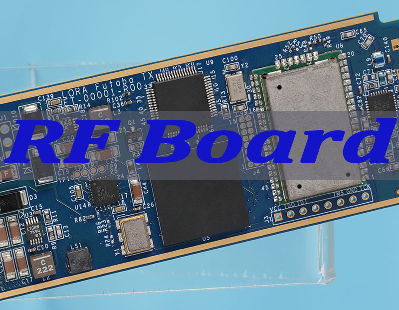
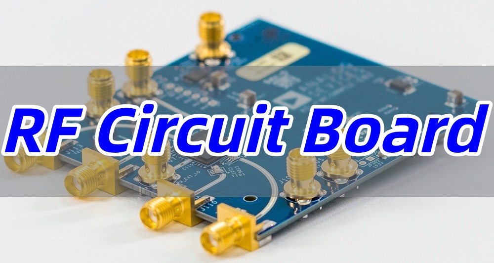
RF HDI circuit board is the critical foundation for high-frequency, high-speed electronics, merging the signal integrity of radio frequency designs with the dense interconnects of HDI technology. This article provides a comprehensive guide to RF HDI boards, addressing key design challenges and showcasing how a manufacturer with full turnkey capabilities ensures success from prototype to final assembly.
Engineers and procurement specialists often face significant hurdles when sourcing advanced RF HDI circuit boards. Common pain points include:
- Struggling to find a manufacturer capable of handling ultra-fine features like 3.3-mil flip-chip pitch.
- Experiencing inconsistent quality or outright rejection from suppliers lacking advanced HDI processes.
- Facing long lead times and poor communication, especially with offshore suppliers that can’t support rapid iteration.
- Dealing with the complexity of managing separate vendors for RF PCB fabrication and assembly.
- Receiving inadequate DFM feedback, resulting in designs that are difficult or costly to manufacture.
At EBest Circuit (Best Technology), we resolve these challenges through our integrated, expert-driven approach. Our solutions are built on:
- Proven Advanced Process Capability: Expertise in HDI PCB manufacturing with 3/3 mil line/space and 4 mil laser micro-drilling.
- Full In-House Control: A true one-stop service encompassing design, advanced packaging substrate manufacturing, fabrication, and assembly under rigorous quality systems.
- Rapid and Reliable Execution: Dedicated engineering support and a 24-hour rapid prototyping service to accelerate your development cycle.
- Turnkey Simplification: A seamless supply chain from component sourcing to final box build, managed by a single point of contact.
- Collaborative Engineering Partnership: Proactive Design for Manufacturability (DFM) analysis to optimize your fine-pitch flip-chip assembly and RF performance before production begins.
Founded in 2006, EBest Circuit (Best Technology) is a certified, full-service PCB and PCBA manufacturer with two decades of specialization in high-technology circuit boards. We operate a 28,900 sq. meter facility equipped with state-of-the-art machinery, from CNC laser drills for high-density via PCB creation to advanced SMT lines for precision assembly. Holding certifications like ISO 9001:2015, IATF 16949, and ISO 13485:2016, we serve over 1,700 clients across 40+ countries with a 97% on-time delivery rate. Our core strength lies in transforming complex RF and HDI designs into reliable, high-performance products. For a consultation on your next project, pls feel free to contact us at sales@bestpcbs.com.
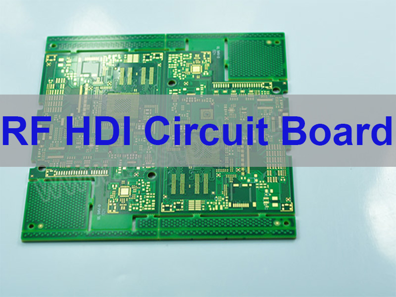
What Is An RF HDI Circuit Board?
An RF HDI circuit board is a sophisticated printed circuit board designed to operate at high frequencies (typically from hundreds of MHz to several GHz) while incorporating High-Density Interconnect (HDI) technology. It combines the need for controlled impedance, low signal loss, and minimal electromagnetic interference of RF design with the space-saving, high-performance interconnects of HDI, which uses micro-vias, fine lines, and multiple via-in-pad structures. This convergence is essential for modern compact, high-speed devices like 5G infrastructure, advanced radar systems, and high-frequency test equipment.
Key characteristics include:
- Advanced Materials: Use of low-loss, stable dielectric substrates like Rogers RO4350B or Taconic, rather than standard FR4.
- Micro-Via Technology: Extensive use of blind, buried, and stacked micro-vias (as small as 4 mils in diameter) to facilitate dense routing.
- Fine Features: Trace/space widths down to 3/3 mils to accommodate fine-pitch ICs and complex routing.
- Impedance Control: Tightly controlled dielectric thickness and trace geometry to maintain specific impedance values (e.g., 50Ω, 100Ω differential).
- Thermal Management: Strategic placement of thermal vias and use of materials with appropriate thermal conductivity to dissipate heat from active components.
In summary, an RF HDI board is the enabling platform for electronics where signal speed, integrity, and component density are all paramount, requiring a manufacturer with precise process control and material expertise.

What Is the Difference Between RF and HDI Circuit Boards?
While both RF and HDI PCBs represent advanced circuit board technologies, they prioritize different design and performance goals. Understanding their distinctions is crucial for selecting the right board for your application and the right manufacturer for your project.
| Feature | RF Circuit Board | HDI Circuit Board | RF HDI Circuit Board |
|---|---|---|---|
| Primary Focus | High-frequency signal performance | High wiring density | High-frequency performance + high density |
| Typical Material | Low-loss laminates | FR4 / high-performance FR4 | Low-loss laminates |
| Main Challenge | Impedance and dielectric loss control | Microvia and fine-line reliability | Impedance control + microvia reliability |
| Common Features | Controlled impedance, ground isolation | Blind/buried vias, via-in-pad | Fine-pitch layout, via-in-pad |
| Process Focus | Material consistency | Laser drilling, sequential lamination | Combined RF + HDI process control |
RF Boards focus on the “quality” of the signal path, minimizing loss and distortion. HDI Boards focus on the “quantity” and efficiency of connections, packing more functionality into less space. An RF HDI Board, the subject of this article, demands expertise in both domains, making the choice of manufacturer—one like EBest Circuit with proven capability in both RF PCB manufacturing and HDI PCB manufacturing—critical to success.
How Many Ground Vias Can Fit Under a Component?
Maximizing ground vias under a component, especially an RF die or a BGA, is vital for providing a low-inductance path to ground, improving thermal dissipation, and shielding. The quantity is determined by a combination of your design rules and the manufacturer’s fabrication limits.
The number is primarily constrained by:
- Via Diameter and Pitch: Our standard micro-drilling capabilities allow for laser-drilled micro-vias as small as 4 mils (0.1mm) in diameter. The minimum via-to-via spacing (pitch) is typically 8-10 mils for these micro-vias. A smaller diameter and tighter pitch allow for more vias.
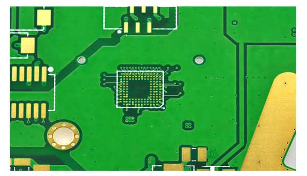
- Pad Size: The component pad size sets the available real estate. Using a via-in-pad design is most effective.
- Aspect Ratio: For thicker boards, the aspect ratio (board thickness to hole diameter) of mechanically drilled vias becomes a limiting factor. Our advanced capability allows an aspect ratio of up to 10:1 for reliable plating.
Illustrative Example:
Under a 1mm x 1mm (40 mil x 40 mil) flip-chip bump pad, assuming a 4 mil via diameter and a 10 mil via pitch (center-to-center), you could theoretically fit a 3×3 array of vias, totaling 9 ground vias. Our engineers can work with you to model the optimal via pattern and quantity to meet both electrical and thermal goals without compromising pad integrity.
What Are the Micro-Drilling Capabilities for RF HDI Boards?
Our micro-drilling capabilities are foundational to producing reliable high-density via PCBs and are a key differentiator for RF HDI work. We employ both mechanical and laser drilling technologies to achieve the precise, small-diameter holes required.
Our key specifications include:
| Drilling Type | Minimum Diameter | Primary Application | Notes |
|---|---|---|---|
| Mechanical Drilling | 8 mils (0.2mm) | Through-holes, larger vias | Standard process for most PTH. |
| Advanced Mechanical Drilling | 6 mils (0.15mm) | High-density through-holes | Used for more demanding designs. |
| Laser Drilling | 4 mils (0.1mm) | HDI micro-vias (blind/buried) | Essential for fine-pitch flip-chip assembly and via-in-pad. |
Supporting Infrastructure:
- Equipment: We utilize advanced CNC laser drill machines to ensure clean, consistent micro-via formation.
- Plating: Our automated plating lines (PTH & PPL) are calibrated to achieve excellent copper deposition in these high-aspect-ratio micro-vias, with a PTH wall thickness of 0.48 mils (12 µm) for HDI designs.
- Inspection: Micro-section analysis is routinely used to verify the quality and plating integrity of micro-vias, ensuring reliability.
Copper Fill vs. Resin Fill: Which Is Better for Vias?
Choosing between copper-filled and resin-filled vias depends on the primary design objective: electrical/thermal performance or surface planarization.
| Criteria | Copper-Filled Vias | Resin-Filled Vias |
|---|---|---|
| Main Purpose | Heat transfer and conductivity | Surface leveling |
| Thermal Performance | Excellent | Low |
| Electrical Conductivity | Conductive | Non-conductive |
| Surface Flatness | Good, may need extra planarization | Excellent |
| Typical Use | Power and RF thermal areas | Fine-pitch BGAs |
| Cost | Higher | Lower |
Our Recommendation:
For RF HDI designs where thermal management under the die is a priority—exactly as highlighted in the client’s request—copper-filled vias are typically the better choice. We can efficiently fill laser micro-vias with copper to create effective thermal conduits. For designs where absolute surface flatness is the overriding concern for solder joint reliability, resin fill is the appropriate option. Our engineering team can advise on the best approach during the DFM review.
Can RO4350B Support High-Density RF Designs?
Yes, absolutely. Rogers RO4350B is an excellent laminate choice for high-density RF designs and is a material we routinely process. It strikes a optimal balance between RF performance and manufacturability, making it suitable for RF HDI circuit boards.
Why RO4350B is suitable for HDI:
- Process Compatibility: Unlike pure PTFE materials, RO4350B is a ceramic-filled hydrocarbon laminate. It has a modifiable surface and can be processed using manufacturing methods similar to FR4, making it compatible with the sequential lamination and laser drilling processes required for HDI.
- Dimensional Stability: It exhibits good dimensional stability, which is crucial for the layer-to-layer registration accuracy needed in multi-layer HDI stack-ups.
- Consistent Dielectric Constant: Its stable Dk (3.48) and low dissipation factor (0.0037) across a wide frequency range ensure predictable impedance and low signal loss in dense designs.
Our Experience with RO4350B:
Our RF board capabilities explicitly list Rogers materials like RO4350B. We handle the specific challenges of these materials, such as ensuring proper hole wall preparation for reliable plating in PTHs. We can fabricate boards with RO4350B across a thickness range of 0.5mm to 3.0mm, supporting various advanced packaging substrate manufacturing needs.
How to Scale RF HDI Designs from Prototype to Production?
Scaling an RF HDI design from a few prototypes to volume production requires careful planning and a manufacturer with scalable processes and a robust supply chain. Here is a structured approach:
- Prototype with Production in Mind: Engage with your manufacturer’s engineering team early. Our DFM analysis for prototypes will flag any features (e.g., ultra-tight tolerances, exotic materials) that may be costly or risky to scale.
- Qualify the Manufacturing Process: Use the prototype phase to not just test the board’s function, but also to audit the manufacturer’s quality. We provide micro-section reports and test data, establishing a quality baseline for production.
- Lock Down Materials and Parameters: Finalize the bill of materials (BOM) for the laminate, prepreg, and surface finish. Document all critical process parameters established during prototyping.
- Plan for Test Fixturing: Prototypes are often tested with flying probes. For volume production, design and procure dedicated test fixtures (e.g., bed-of-nails) during the prototyping lead time to avoid delays.
- Implement Statistical Process Control (SPC): In production, we monitor key parameters (e.g., impedance, copper thickness) using SPC charts to detect and correct process drift before it causes defects.
- Leverage the Manufacturer’s Volume Capacity: Our monthly production capacity of 260,000 square feet is designed to absorb volume orders without sacrificing the lead time or quality standards set during prototyping.
How to Ensure Reliability in Advanced Packaging Substrates?
Ensuring reliability in advanced packaging substrates—a category that includes complex RF HDI boards—requires a holistic approach focused on material science, process control, and rigorous testing.
Our reliability assurance framework is built on four pillars:
- Material Selection and Compatibility: We ensure all materials in the stack-up (core, prepreg, copper, solder mask) have matched coefficients of thermal expansion (CTE) as closely as possible to minimize stress during thermal cycling. We only source materials from qualified, certified suppliers.
- Robust Process Engineering:
- Desmear and Plating: For HDI micro-vias, we employ optimized plasma desmear and electrolytic plating processes to ensure a void-free, high-integrity copper connection, critical for thermal and electrical reliability.
- Lamination Control: Precise control of lamination pressure, temperature, and vacuum is maintained to prevent delamination.
- Comprehensive Inspection and Testing:
- Electrical Testing: 100% electrical test (using flying probe or fixture) for continuity and isolation.
- Automated Optical Inspection (AOI): For detecting surface defects on inner and outer layers.
- Micro-sectional Analysis: Destructive cross-sectioning to verify via plating quality, layer alignment, and interlayer bonding.
- Reliability Stress Testing: We can perform thermal shock, thermal cycling, and highly accelerated life testing (HALT) on samples to validate product lifetime under simulated operating conditions.
- Certification and Standards Adherence: Our production follows IPC-6012 Class 2/3 standards for rigid boards and IPC-6013 for flex circuits. Our ISO 9001, ISO 13485, IATF 16949, AS9100D certifications mandates a process-focused approach to defect prevention and continuous improvement, inherently boosting long-term reliability.
To sum up, RF HDI circuit boards are the sophisticated engines powering the next generation of high-frequency, miniaturized electronics. This article has explored their defining characteristics, key manufacturing considerations, and the path from prototyping to reliable production.
Choosing the right partner is paramount. EBest Circuit (Best Technology) combines 20 years of precision manufacturing expertise with a full turnkey service model. From handling your 3.3-mil flip-chip pitch and high-density via PCB challenges to providing expert DFM on your advanced packaging substrate design, we ensure rigorous quality at every step—from the initial prototype to volume assembly.
Pls feel free to contact our engineering sales team anytime at sales@bestpcbs.com for a comprehensive quote and DFM analysis.
FAQs About RF HDI Circuit Board
Q: Can Your PCB Supplier Handle 3.3-mil Flip-Chip Pitch?
A: Yes, we can. Handling a 3.3-mil (approx. 0.084mm) flip-chip pitch is a demanding but achievable requirement that falls under our HDI and advanced packaging capabilities. It requires our most precise laser drilling for micro-vias (4 mil) and expert solder mask control to define such fine pad separations. Success depends on a collaborative DFM review to optimize the pad design, solder mask dam, and via-in-pad structure. We have the equipment and process expertise to support this level of fine-pitch flip-chip assembly.
Q: What is your minimum line width/space for HDI designs?
A: For our advanced HDI process, our standard minimum line width and space is 3/3 mils (0.075/0.075mm). This capability is clearly listed in our FR4 PCB capability table under the “HDI” specification and is essential for routing the escape patterns from fine-pitch components used in RF HDI circuit boards.
Q: What impedance control tolerance can you achieve?
A: We offer tight impedance control for RF designs. For impedance values greater than 50Ω, we maintain a tolerance of ±10%. For values of 50Ω or less, we control to within ±5Ω. This is achieved through precise control of dielectric thickness, etch profile, and material selection, such as Rogers RO4350B.
Q: What is your standard and fastest lead time for an RF HDI prototype?
A: Lead time depends on layer count and complexity. For a standard specification 4-layer FR4-based prototype, our normal service is 10 days, with a 48-hour fastest service. For RF boards using specialized materials like Rogers, the typical sample lead time is 7-9 days. We always recommend contacting us with your Gerber files for the most accurate quote and expedited options.