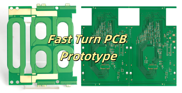
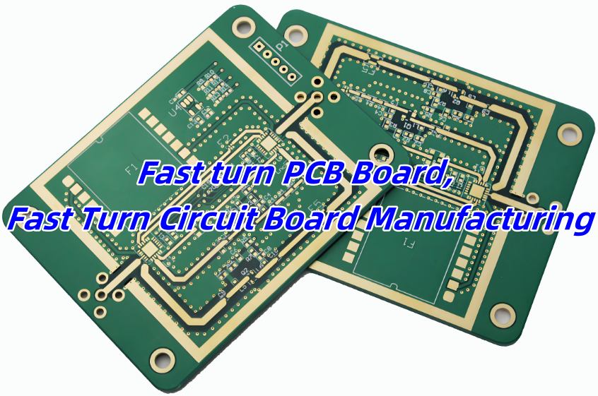
What Is a Fast Turn PCB Board?
A fast turn PCB board is a printed circuit board manufactured and delivered in a short time, typically within 24 to 72 hours. These quick deliveries help speed up product development, especially during prototyping and pre-production stages. It’s a solution many engineers rely on when time is tight.
Engineers use fast turn PCBs for product validation. They want to see if a new circuit design performs well before moving to mass production. So, getting a board in days instead of weeks can make a huge difference.
What Are the Benefits of Fast Turn PCB Orders?
Ordering a fast turn PCB board brings several advantages to the table.
First, it speeds up your product timeline. You don’t need to wait weeks to test your circuit. If changes are needed, you can get a revised board quickly and keep things moving forward.
Second, it helps reduce project risks. The faster you test, the faster you detect potential design errors. Early detection saves money and prevents delays.
Third, it improves decision-making. With working samples in hand, your team can test real performance. It’s better than guessing or using simulation data only.
Lastly, fast turn options give your company a competitive edge. Getting to market faster often means better sales and stronger customer trust.
Best Technology’s Typical Turnaround Time for Fast Turn PCBs
At Best Technology, we understand the value of time. That’s why we’ve optimized our process to support urgent PCB orders.
For standard 2-layer fast turn PCBs, we usually deliver in 24 to 48 hours. For 4-layer boards, it may take 48 to 72 hours depending on complexity. Our team works around the clock to meet those deadlines.
Even for more complex boards — such as HDI or metal-core PCBs — we still maintain one of the quickest turnaround times in the industry. And we don’t compromise on quality. Each board goes through full inspection and electrical testing before it reaches you. The detailed turnaround time is:
| Prototype(<1m²) | Layers | Normal Service | Expedited Service |
| FR4 PCB | 1 Layer | 3-4 days | 24 hours |
| 2 Layers | 4-6 days | 24 hours | |
| 4 Layers | 8-10 days | 48 hours | |
| 6 Layers | 8-10 days | 72 hours | |
| 8 Layers | 10~14 days | 72-96 hours | |
| 10 Layers | 14-18 days | 72-96 hours | |
| HDI (1+N+1 2+N+2) | 2.5 – 3.5weeks | TBD (depend on design) |
We don’t just print boards fast. We manage the process with strict planning, from materials to delivery. That’s why so many clients come back to us for every new project.
Factors That Affect the Turnaround Time of Prototypes
Even though we push for speed, several factors can influence how long a fast turn circuit board takes to produce. Knowing these helps avoid delays.
- Circuit Board Design and Test Procedures
The design stage impacts everything. A simple, well-structured layout speeds up processing. Complex routing, fine-pitch components, or tight spacing can add extra review time.
Test procedures matter too. If a special test is needed, like impedance control or functional test setup, it adds to the schedule. Providing clear instructions in advance helps us prepare and avoid delays.
- Lamination Cycles
For multilayer boards, each lamination cycle takes time. A 4-layer multi-layer board needs one cycle, while an 8-layer may need several. More layers mean longer pressing times and more careful control.
Quick builds still go through these steps. We just start immediately and plan shifts to manage it faster. That’s why sharing the full stack-up early is so important.
- Via-in-Pad Plated Over
Via-in-pad designs are helpful for high-density layouts. But they add a few extra steps in production. We need to drill, plate, and fill those vias carefully. After that, we cap and flatten them before plating the surface.
This extra effort adds time compared to standard vias. If your board uses VIPPO, it’s best to let us know upfront so we can fast-track these processes.
- Fabrication Drawing Specifications
Precise drawings help avoid back-and-forth communication. If drawings are unclear or missing details like dimensions, tolerances, or hole types, we’ll need to clarify before production.
Clear drawings lead to fast fabrication. They also reduce the risk of mistakes. That’s why we suggest using IPC-2581 or Gerber X2 format with notes included.
- Surface Finish
Surface finish choice also plays a role. ENIG, OSP, HASL, or hard gold all have different process times. For example, ENIG takes longer than HASL because it involves two plating steps.
If speed matters most, we can recommend the best finish based on your needs. Some finishes can still meet performance goals while shaving off hours from the process.
- Assembly Drawings and Notes
If you also need PCB assembly, complete documentation is key. Missing part placements, unclear polarity marks, or unreferenced BOM items slow everything down.
Providing all files in one go—BOM, pick and place, centroid file, and notes—helps avoid delays. When everything’s ready, our SMT line can move fast and precise.
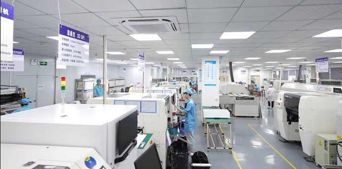
Fast Turn Circuit Board Manufacturing
Manufacturing a fast turn circuit board isn’t about rushing. It’s about knowing how to work smart, reduce waste, and prevent rework.
At Best Technology, we keep a reserve stock of core materials and prepreg. That way, we can start production immediately without waiting for supply.
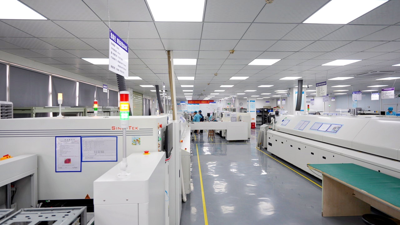
We also use automatic routing, inline AOI, and robotic drilling machines to keep operations smooth. Our teams work in shifts, so production doesn’t stop, even at night or on holidays.
Every department is synchronized. CAM engineers review your files fast, material control prepares the stack-up, and QA teams check every step. That’s how we manage fast output without losing accuracy.
We also run a parallel system for urgent jobs. These special jobs go into our “fast-lane” line, separated from standard orders. This ensures time-sensitive boards don’t get stuck behind large-volume orders.
Why Should You Choose Best Technology as Your Preferred Partner?
Choosing a fast turn PCB partner isn’t just about delivery speed. It’s about trust, communication, and consistent results. Best Technology stands out because we offer more than just fast service.
- Experienced team: We’ve been in this field for over 18 years. Our engineers know what works and how to prevent problems early.
- Clear communication: Our team responds quickly. We give you updates, clarify questions, and solve problems before they become delays.
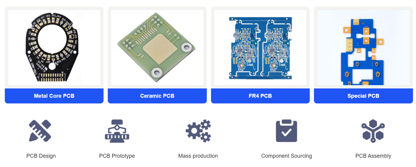
- Flexible production: Whether you need 1 board or 10,000, we scale easily. We also support special needs like rigid-flex, metal core, or ceramic boards with fast turn options.
- Global shipping: We work with trusted logistics partners. Boards reach you safely and on time, even across borders.
- Reliable quality: Every board goes through full inspection, AOI, flying probe, and E-test. Even fast jobs go through our strict quality checks.
When you work with Best Technology, you get speed, support, and security in every step. That’s why companies in medical, industrial, and automotive industries continue to rely on us.