SMT PCB board manufacturing is the foundation of modern electronics production, enabling compact layouts, stable electrical performance, and scalable assembly across a wide range of applications. This article explains what an SMT PCB board is, how SMT differs from other assembly technologies, what processes and board types are involved, and how quality is controlled in real manufacturing environments.
Understanding how SMT PCB board manufacturing actually works is essential for engineers and procurement teams alike. As an established manufacturer with over 20 years of experience in the SMT PCB board industry, EBest Circuit (Best Technology) is committed to becoming a reliable one-stop PCBA service provider. Our engineering and sales teams possess strong, practical knowledge of SMT manufacturing processes and production workflows, enabling clear technical communication at every project stage. We also excel in providing free DFM review and process adaptation suggestions, helping engineers reduce risk and improve manufacturability early in the design phase.
To prepare accurate SMT placement programs, a complete BOM list, a clear silkscreen reference designator drawing, and a correct pick-and-place (centroid) file are all essential inputs for the assembly process. If you require any related consultancy services or technical support, please feel free to contact us at sales@bestpcbs.com and provide these files for review.
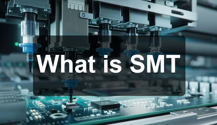
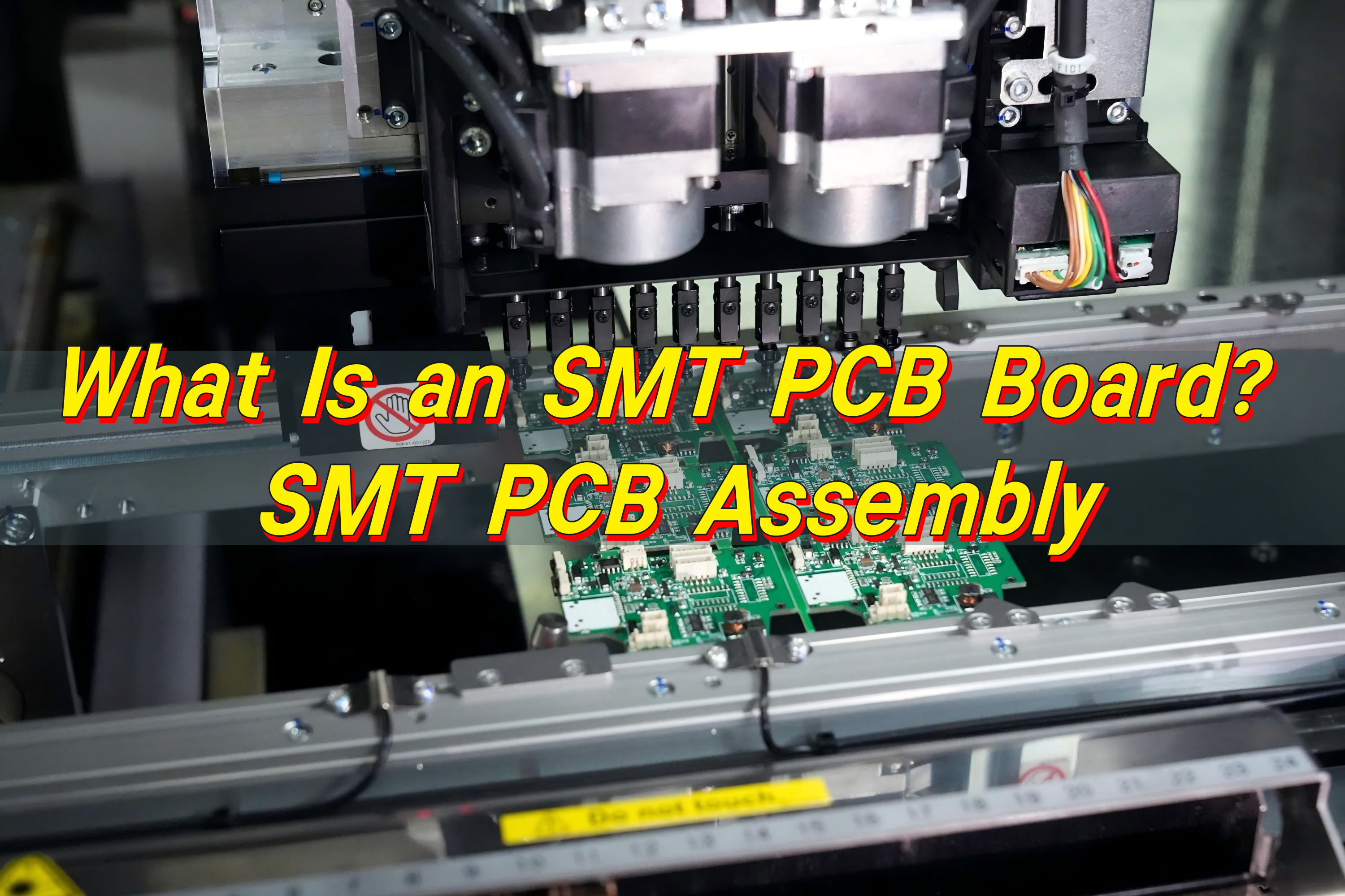
What Is a SMT PCB?
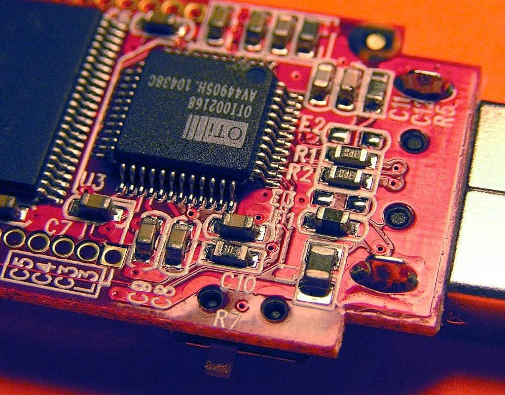
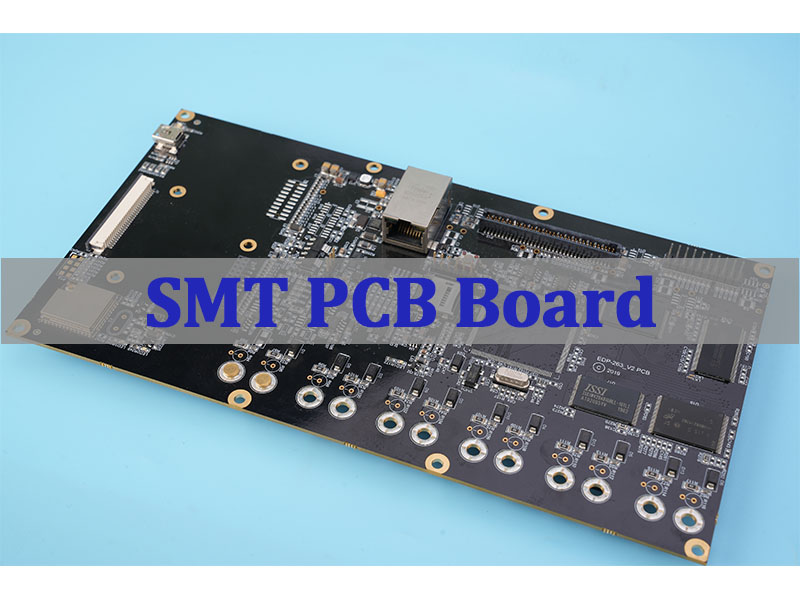
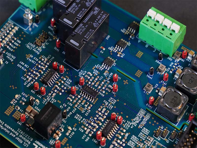
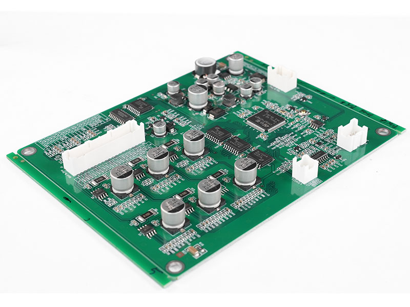
A SMT PCB is a printed circuit board designed and assembled using Surface Mount Technology, where electronic components are mounted directly onto the surface of the PCB rather than inserted through drilled holes. In SMT PCB manufacturing, components are placed with high precision and soldered through controlled reflow processes.
From a manufacturing perspective, SMT in PCB manufacturing is not just a placement method. It is a complete system that integrates PCB design rules, solder paste printing, component placement accuracy, thermal profiling, and inspection strategy. Each step affects yield, reliability, and repeatability.
In practice, SMT PCB boards allow higher component density, shorter signal paths, and better electrical consistency compared to older assembly methods, which is why SMT has become the dominant technology in electronics production today.
What Is the Difference Between SMD and SMT PCB?
SMD and SMT are closely related but refer to different aspects of the same process. SMD (Surface Mount Device) refers to the components themselves, while SMT PCB refers to the assembly process used to mount those components onto the PCB.
From an engineering standpoint, confusion between SMD and SMT often leads to incomplete specifications. Engineers must define not only the component package (SMD) but also the assembly capability, inspection method, and rework strategy associated with SMT PCB manufacturing.
In real builds, the distinction matters because component selection, pad design, and SMT stencil thickness must all align with the SMT process window. Treating SMT PCB assembly as interchangeable with component choice alone is a common source of early-stage defects.
Why Is SMT PCB Board Used?
The SMT PCB board is used because it supports the performance, size, and manufacturing efficiency requirements of modern electronics. SMT enables smaller footprints, lighter assemblies, and higher functional integration.
From a production perspective, SMT PCB boards allow consistent automation, improved solder joint quality, and faster assembly cycles when properly engineered. These benefits are not theoretical; they directly affect yield stability and cost control.
In real-world manufacturing, SMT PCB board usage is driven by the need to balance electrical performance, thermal behavior, and scalability. This is why SMT is used across consumer electronics, industrial control, automotive systems, medical devices, and communication equipment.
What Processes Are Involved in SMT PCB Board Assembly?
SMT PCB board assembly involves a tightly controlled sequence of processes, each of which must be executed consistently to achieve reliable results.
Key processes include:
- Solder paste stencil printing with controlled volume and alignment
- High-accuracy component placement using pick-and-place systems
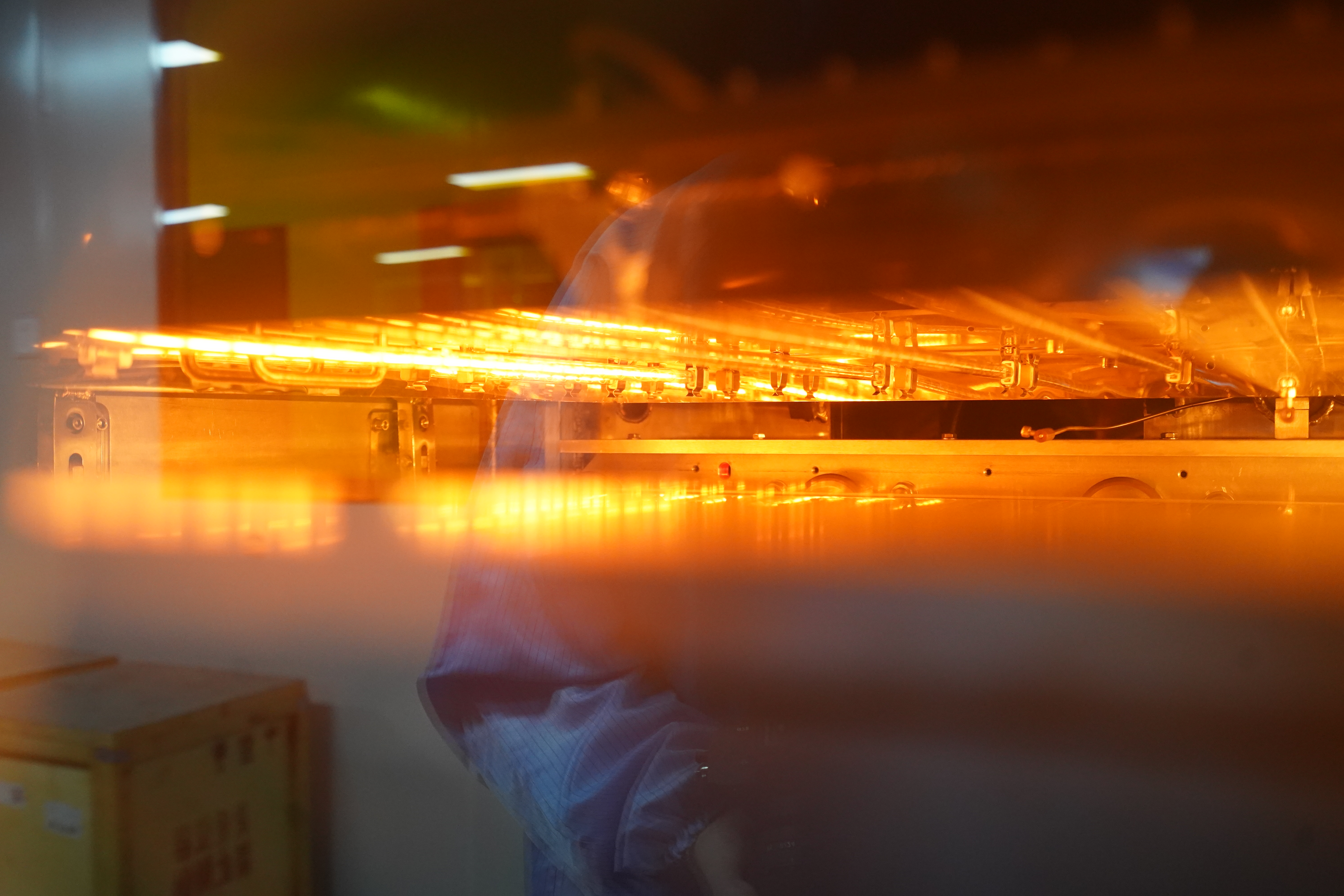
- Reflow soldering with defined thermal profiles
- Automated Optical Inspection (AOI) and functional checks
- Rework and verification when required
From an engineering perspective, none of these steps can be optimized in isolation. Paste formulation, placement accuracy, and reflow profile must work together as a system.
In real production, stable SMT PCB board assembly comes from process discipline, not equipment alone. Manufacturers that focus only on speed or cost often sacrifice long-term reliability.
How Does PCB Board SMT Differ From THT and DIP Assembly?
PCB board SMT differs fundamentally from through-hole technologies such as THT and DIP assembly in both structure and manufacturing behavior. SMT mounts components on the surface, while THT and DIP require drilled holes and manual or wave soldering processes.
| Assembly Method | SMT PCB Board | THT Assembly | DIP Assembly |
|---|---|---|---|
| Component Mounting | Surface-mounted | Leads inserted through holes | Dual in-line through holes |
| Board Density | Very high | Medium | Low |
| Automation Level | Fully automated | Semi-automated | Mostly manual |
| Assembly Speed | Fast | Moderate | Slow |
| Mechanical Strength | Moderate | High | High |
| Rework Complexity | Higher | Easier | Easier |
| Typical Applications | HDI, consumer, industrial, medical | Power, connectors | Legacy designs, prototypes |
| Scalability | Excellent | Limited | Poor |
From a manufacturing viewpoint:
- SMT supports higher density and automation
- THT and DIP provide stronger mechanical anchoring for large components
- SMT is more sensitive to thermal control and paste consistency
In real assembly lines, board assembly SMT DIP PCB and board assembly SMT THT PCB processes are often combined on the same board. Managing these hybrid builds requires careful sequencing to avoid solder defects or component damage.
What Types of Boards Commonly Use SMT PCB Board Technology?
SMT PCB board technology is used across a wide range of board types, not just standard FR4 designs.
Common applications include:
- HDI multilayer boards with fine-pitch components
- Aluminum-based PCBs for LED and power applications
- Complex multilayer control boards
- High-speed and high-density digital systems
From an engineering standpoint, each board type introduces different thermal, mechanical, and inspection challenges. SMT PCB manufacturing must adapt process parameters accordingly.
In real manufacturing, suppliers with limited board experience often struggle when moving beyond standard FR4 SMT assemblies.
How Do SMT PCB Board Manufacturers Control Quality and Reliability?
Professional SMT PCB board manufacturers rely on process control rather than end-stage inspection alone. Quality must be built into each manufacturing step.
Effective control methods include:
- Incoming material verification and traceability
- First Article Inspection (FAI)
- AOI at multiple stages
- Controlled reflow profiling
- MES-based lot and process tracking
From a reliability perspective, these controls ensure that each SMT PCB board performs consistently across production batches.
In practice, SMT PCB board factories with weak documentation or incomplete traceability often cannot support regulated or high-reliability applications.
Why Choose a China SMT PCB Board Manufacturer for Production?
A qualified China SMT PCB board manufacturer offers advantages beyond cost, including supply chain maturity, integrated PCB and PCBA capability, and flexible production scaling.
From an engineering and procurement viewpoint, China-based manufacturing supports:
- Faster component sourcing and substitution handling
- Closer integration between PCB fabrication and SMT assembly
- Shorter lead times for both prototypes and volume builds
That said, not all SMT PCBA suppliers operate at the same level. Engineering involvement, documentation quality, and process transparency are what separate reliable circuit assembly manufacturers from purely price-driven ones.
Why Choose EBest Circuit for SMT PCB Board Manufacturing?
EBest Circuit (Best Technology) approaches SMT PCB board manufacturing as an engineering service rather than a transactional process. We focus on execution discipline, traceability, and long-term manufacturability.
Our strengths include:
- In-house PCB fabrication and SMT assembly
- Dedicated engineering involvement throughout the build
- Clear process documentation and MES-based traceability
- Support for complex, mixed-technology assemblies
- Stable delivery backed by real production capability
We do not compete by cutting corners or racing to the lowest price. Instead, we deliver consistent SMT PCB board manufacturing that engineers and procurement teams can rely on. And we attach great importance to customer experience and believe that long-term success is driven by delivering real value through both before and after sales service. From initial technical discussions to post-delivery support, our goal is to ensure every customer enjoys a smooth, transparent, and dependable project experience. For technical discussions or project inquiries, please contact us at sales@bestpcbs.com.
FAQ: SMT PCB Board
What Are the Disadvantages of SMT?
SMT requires tighter process control and is more sensitive to thermal and paste variations compared to through-hole assembly.
Is SMT the Same as SMD?
No. SMD refers to the component, while SMT refers to the assembly process used to mount it.
Can SMT Components Be Repaired?
Yes. With proper equipment and procedures, SMT components can be reworked or replaced.
How Do You Remove SMD Components?
SMD components are typically removed using controlled hot air or rework stations to avoid PCB damage.