

Just like FR4 PCB, we can also make boards with more than 2 layers of traces and we named it “Multi Layers MCPCB“. The structure is similar with FR4 Multi Layers, but it much more complex to make.
You can populated more components on the boards, put signal and ground layer into seperated layers, to achieve better performance in electrical performance.
Compared with normal FR4, this sturcture need more technology and experience on laminating of more than two layers together with metal core and the cost is much higher than 2 layers MCPCB or double sided MCPCB.
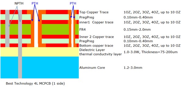
Structure of Multi Layers MCPCB
Capability of Multi Layers MCPCB
- Base material: Aluminum/Copper/Iron Alloy
- Thermal Conductivity (dielectrial layer): 0.8, 1.5, 2.0, 3.0 W/m.K.
- Board Thickness: 0.8mm~3.0mm(0.02″~0.12″)
- Copper thickness: 0.5 OZ, 1.0 OZ, 2.0 OZ, 3.0 OZ
- Outline: Routing, punching, V-Cut
- Soldermask: White/Black/Blue/Green/Red Oil
- Legend/Silkscreen Color: Black/White
- Surface finishing: Immersion Gold, HASL, OSP
- Max Panel size: 600*500mm(23.62″*19.68″)
- Packing: Vacuum/Plastic bag
- Samples L/T: 15~18 Days
- MP L/T: 15~20 Days
FAQs
1. What is a multi-layer MCPCB and how does it differ from standard FR4?
A multi-layer MCPCB consists of multiple copper conductive layers separated by high-thermal-conductivity dielectric layers, all bonded to a metal base (usually Aluminum or Copper). Unlike standard FR4, which relies on the epoxy glass substrate for structure, an MCPCB uses the metal base as a heat sink. While FR4 is an insulator with poor thermal management, the metal core in an MCPCB allows for heat dissipation rates that are significantly higher, making it essential for high-power electronics.
2. What are the typical thermal conductivity levels for multi-layer MCPCBs?
The thermal performance of a multi-layer MCPCB is primarily determined by the dielectric layer rather than the metal base itself. Standard dielectric materials offer conductivity between 1.0 W/mK and 3.0 W/mK. However, high-performance multi-layer stacks used in automotive or aerospace applications can reach 4.0 W/mK to 8.0 W/mK. Choosing the right dielectric is a balance between thermal efficiency and the breakdown voltage required for the circuit.
3. How many layers can be integrated into a Metal Core PCB?
Technically, “multi-layer” in the context of MCPCBs typically refers to 2-layer or 4-layer configurations. While it is possible to go higher, the complexity increases significantly because all heat must eventually pass through the dielectric layers to reach the metal base. In a 4-layer stack, the inner layers are further from the heat sink, which can lead to thermal bottlenecks if the design does not utilize thermal vias effectively.
4. Can you use plated through-holes (PTH) in a multi-layer MCPCB?
Yes, but the process is more complex than with standard PCBs. To prevent short-circuiting the signals to the metal core, the metal base must be pre-drilled and filled with an epoxy resin before the copper layers are laminated. Then, a smaller hole is drilled through the resin plug and plated. This creates an “insulated via” that allows signals to pass through the metal core safely.
5. What are the main applications for multi-layer MCPCB designs?
Multi-layer MCPCBs are the go-to solution when space is limited but power density is high. Common applications include:
- Automotive: LED headlight systems and power converters (EV/HEV).
- Power Supplies: High-voltage regulators and heavy-duty industrial rectifiers.
- Aerospace: Power distribution units where weight and heat must be managed simultaneously.
- Medical: High-intensity surgical lighting and imaging equipment.
6. What are the manufacturing challenges of multi-layer MCPCBs?
The primary challenge is coefficient of thermal expansion (CTE) mismatch. Metal bases (Aluminum/Copper) expand at different rates than the copper traces and dielectric during the lamination process. This can lead to delamination or bowing of the board. Precise control over the pressing cycle and the use of specialized “no-flow” or “low-flow” prepregs are required to ensure the structural integrity of the multi-layer stack.