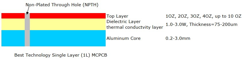
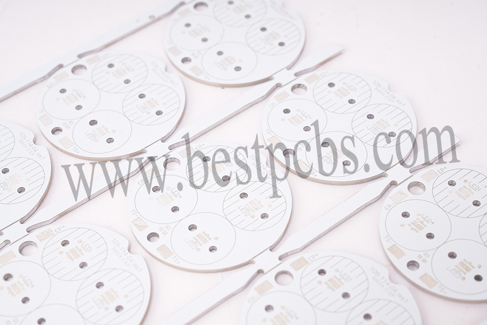
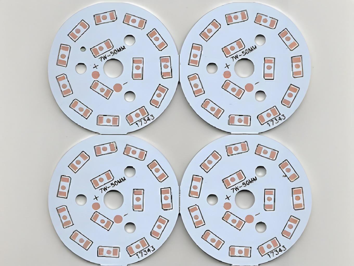
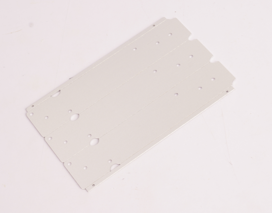
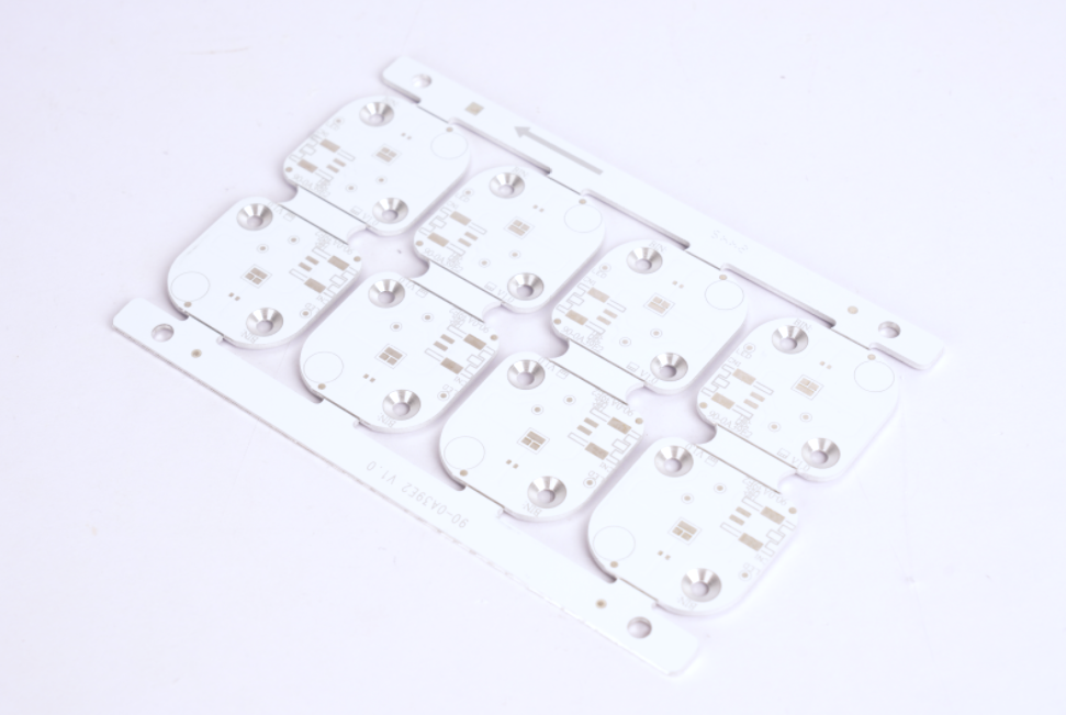
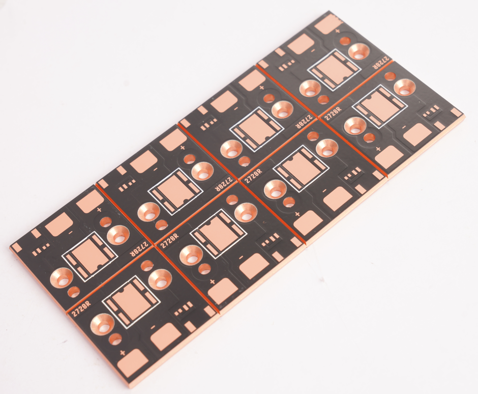
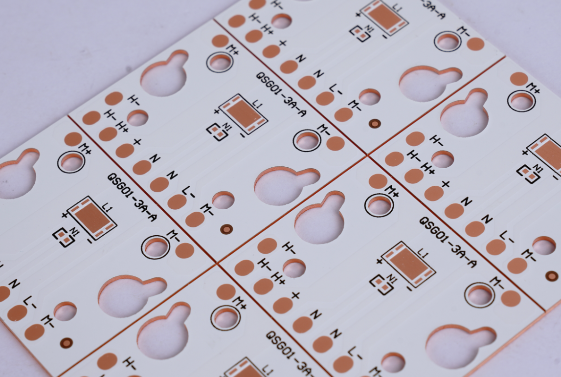
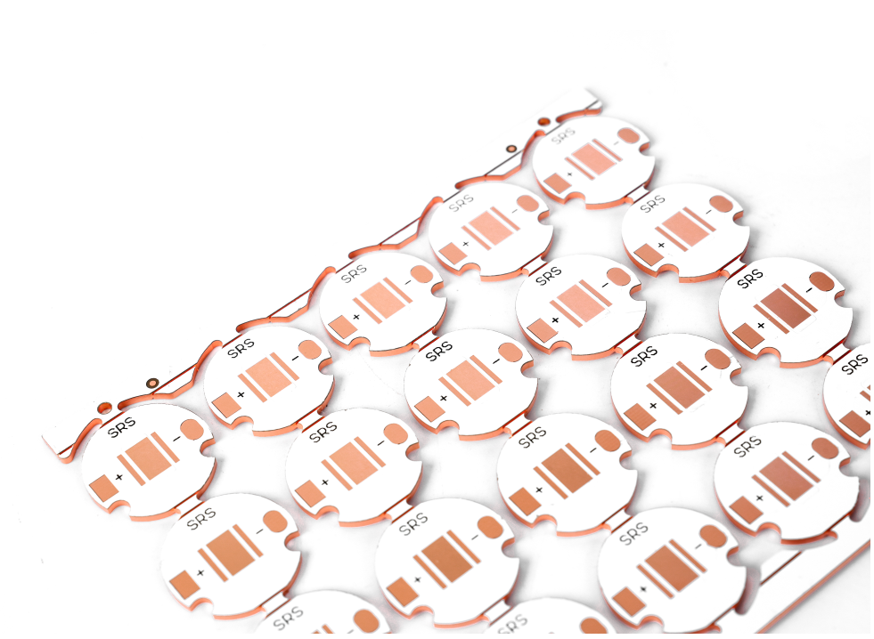
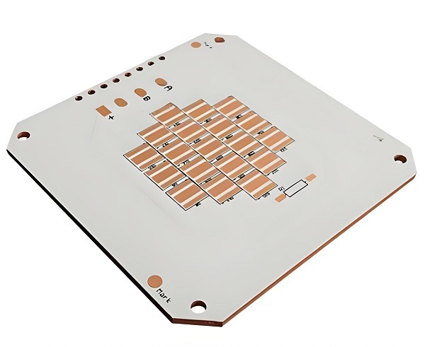
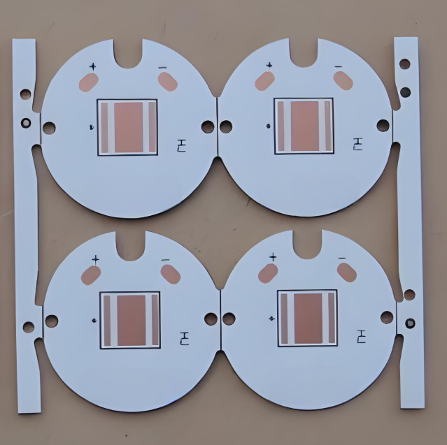
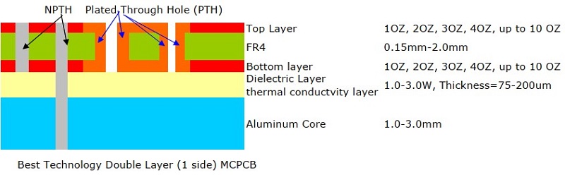
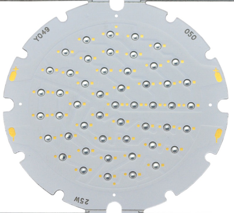
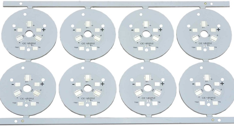
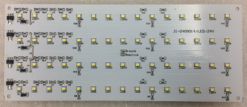
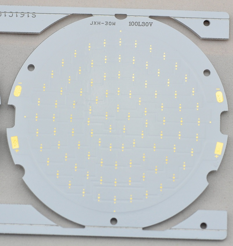
A simple layer single sided MCPCBconsists of a metal base (usually aluminum, or copper alloy), Dielectric (non-conducting) Layer, Copper Circuit Layer, IC components and solder mask.
The prepreg dielectric provides excellent heat transfer from the foil and components to the base plate, while maintaining excellent electrical isolation. The base aluminum/copper plate gives the single-sided substrate mechanical integrity, and distributes and transfers the heat to a heat sink, mounting surface or directly to the ambient air.
The Single-Layer MCPCB can be used with surface mount and chip & wire components, and provides much lower thermal resistance than FR4 PWB. The metal core provides lower cost than ceramic substrates, and allows much larger areas than ceramic substrates.
Copper thickness: 0.5 OZ, 1.0 OZ, 2.0 OZ, 3.0 OZ, up to 10 OZ
Outline: Routing, punching, V-Cut
Soldermask: White/Black/Blue/Green/Red Oil
Legend/Silkscreen Color: Black/White
Surface finishing: Immersion Gold, HASL, OSP
Max Panel size: 600*500mm(23.62″*19.68″)
Packing: Vacuum/Plastic bag
Samples L/T: 4~6 Days
MP L/T: 5~7 Days
Single Layer MCPCB FAQs
1. What is a single layer MCPCB?
A single layer MCPCB consists of a metal base (typically aluminum or copper), a non-conductive dielectric layer, and a copper circuit layer. Unlike standard PCBs, the metal core acts as a primary heat sink, moving thermal energy away from high-power components to the environment or an external cooling system.
2. How does a single layer MCPCB differ from a standard FR4 PCB?
The primary difference is the substrate material. While FR4 uses fiberglass and epoxy, an MCPCB uses a metal base. This allows MCPCBs to have significantly higher thermal conductivity. While a standard FR4 board typically has a conductivity of around 0.25 W/mK, a single layer MCPCB can range from 1.0 W/mK to 9.0 W/mK depending on the dielectric material used.
3. What are the typical applications for single layer MCPCBs?
Single layer MCPCBs are most commonly used in the LED lighting industry (street lights, automotive headlamps, and backlight units) because LEDs generate significant heat that can degrade performance if not dissipated. They are also widely used in power conversion, solid-state relays, and the automotive sector for motor control modules.
4. Can you have plated through-holes (PTH) on a single layer MCPCB?
Generally, no. In a standard single layer MCPCB, the metal base is conductive, so through-holes would cause a short circuit between the signal layer and the base. Components are typically Surface Mount Devices (SMD). If through-hole components are required, specialized “COB” (Chip on Board) or complex insulated hole processes are needed, which significantly increases cost.
5. What are the layers of a single layer MCPCB?
A standard stack-up includes four main layers:
Solder Mask: Protects the copper circuit.
Circuit Layer: The copper foil used for traces.
Dielectric Layer: The most critical part; it provides electrical insulation while facilitating heat transfer.
Metal Substrate: Usually 1.0mm to 3.2mm of Aluminum (5052 or 6061) or Copper.
6. Is aluminum or copper better for the metal core?
Aluminum is the most popular choice because it is cost-effective and provides excellent thermal dissipation for most applications. Copper offers even higher thermal conductivity but is much heavier and more expensive. Copper is usually reserved for extremely high-power density applications where aluminum’s performance is insufficient.
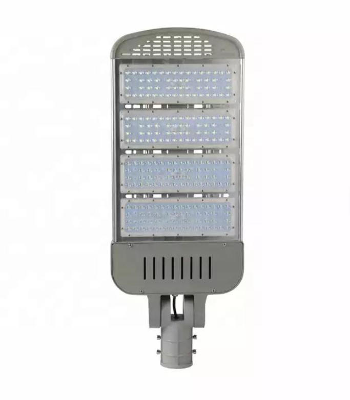
Looking for High Thermal Conductivity MCPCB for LED Street Light? Choose EBest First for Premium Quality & Stable Performance
When selecting High Thermal Conductivity MCPCB for LED Street Light, core parameters directly determine the reliability and lifespan of your LED street lighting. EBest’s products are tailored to solve thermal management pain points in LED street lights, with industry-leading specifications.
Our High Thermal Conductivity MCPCB for LED Street Light features: Thermal conductivity ranging from 2.0W/(m·K) to 12W/(m·K), 6061-T6 aluminum alloy base, 50-100μm nano-ceramic dielectric layer, 2-4oz electrolytic copper foil, and operating temperature range of -40℃ to 125℃.
All products pass strict thermal cycle and insulation tests, ensuring stable performance in harsh outdoor environments. For your LED street light projects, choose EBest’s High Thermal Conductivity MCPCB—contact us to place your order today.
MCPCB for LED Street Light
Why Choose EBest for High Thermal Conductivity MCPCB for LED Street Light?
Quality Assurance: We adopt automatic vacuum lamination and AOI detection, achieving a production yield of over 98.5%. All products comply with international standards and undergo rigorous reliability testing.
Fast Delivery: Our vertically integrated supply chain enables small-batch delivery in 7 days and mass production in 15–20 days, eliminating delays in your project timeline.
Stable Supply Chain: Long-term partnerships with top material suppliers ensure a steady supply of core raw materials, avoiding production interruptions caused by material shortages.
Professional Service: Our technical team provides one-on-one DFM (Design for Manufacturability) advice, optimizing designs for manufacturability and solving technical issues throughout the project cycle.
What Are the Core Pain Points of High Thermal Conductivity MCPCB for LED Street Light, and How Does EBest Solve Them?
Many users face challenges such as poor thermal dissipation, inconsistent production quality, and supply chain risks when using High Thermal Conductivity MCPCB for LED Street Light. EBest addresses these pain points with targeted solutions.
Pain Point 1: Overheating leads to LED light degradation and shortened lifespan. Solution: Our MCPCB uses high-quality thermally conductive dielectric layers, reducing thermal resistance to ≤5℃/W and keeping the LED junction temperature below 85℃.
Pain Point 2: Inconsistent batch production affects product reliability. Solution: We implement strict SPC (Statistical Process Control) and 100% AOI detection to ensure consistent quality across all batches.
Pain Point 3: Long delivery times delay project schedules. Solution: Our in-house production lines and optimized supply chain reduce delivery times by 30% compared to industry averages.
Pain Point 4: Poor insulation performance poses safety hazards. Solution: All our MCPCBs pass 25KV insulation withstand voltage tests, meeting outdoor safety standards. Choose EBest to solve all your High Thermal Conductivity MCPCB for LED Street Light pain points.
What Is High Thermal Conductivity MCPCB for LED Street Light, and Why Is It Essential?
High Thermal Conductivity MCPCB for LED Street Light is a specialized metal-core PCB designed for outdoor LED street lighting, consisting of a metal base, thermally conductive dielectric layer, and copper circuit layer.
LED street lights convert only 20–30% of electrical energy into light, with 70% or more converted into heat. Traditional FR-4 PCBs (with a thermal conductivity of 0.3–0.5W/(m·K)) cannot dissipate heat efficiently, leading to rapid light degradation.
High thermal conductivity MCPCBs solve this issue by transferring heat quickly from LED chips to heat sinks, extending the LED lifespan to over 50,000 hours and ensuring stable brightness.
How to Choose the Right Thermal Conductivity for High Thermal Conductivity MCPCB for LED Street Light?
How to Choose the Right Thermal Conductivity for High Thermal Conductivity MCPCB for LED Street Light?
The right thermal conductivity depends on your LED street light’s power and operating environment. For most municipal street lights (30–50W), 2.0–4.0W/(m·K) MCPCBs are sufficient.
For high-power street lights (50–100W) or areas with high ambient temperatures, choose 4.0–8.0W/(m·K) products. For extreme outdoor environments, 8.0–12.0W/(m·K) high-grade MCPCBs are recommended.
EBest’s technical team can help you select the optimal thermal conductivity based on your specific project requirements, ensuring both cost-effectiveness and performance.
What Are the Key Materials for High Thermal Conductivity MCPCB for LED Street Light?
The performance of High Thermal Conductivity MCPCB for LED Street Light depends on three core materials: the metal base, dielectric layer, and copper foil.
Metal Base
We use 6061-T6 aluminum alloy (with a thermal conductivity of ≥200W/(m·K)) for most projects, balancing thermal performance and cost. For high-end applications, copper or copper-molybdenum alloy bases are available.
Dielectric Layer
Nano-ceramic dielectric layers (50–100μm) are used, offering high thermal conductivity and insulation. They reduce thermal resistance while ensuring electrical safety.
Copper Foil
2–4oz electrolytic copper foil is standard, supporting high current and reducing voltage drop. Heavy copper (4oz+) is available for high-power LED street lights.
How Does High Thermal Conductivity MCPCB Improve LED Street Light Lifespan?
It is an industry consensus that for every 10℃ increase in LED junction temperature, the lifespan decreases by 50%. High Thermal Conductivity MCPCB for LED Street Light directly reduces the junction temperature, significantly extending the lifespan.
Our MCPCB reduces thermal resistance by 40% compared to traditional FR-4 PCBs. In practical tests, LED street lights using our MCPCB maintained 95% light flux after 6,000 hours of continuous operation.
This not only reduces maintenance costs but also enhances the reliability of your LED street lighting projects.
What Are the Top 4 Industry Applications of High Thermal Conductivity MCPCB for LED Street Light?
High Thermal Conductivity MCPCB for LED Street Light is widely used in outdoor lighting and related fields. Below are four popular industry applications with real-world cases.
1. Municipal Road Lighting
Case: Singapore HDB street light project. Our 2.0W/(m·K) MCPCB was used, achieving 98.7% uptime and reducing maintenance frequency by 60%.
2. Highway Lighting
Case: European highway lighting project. High-power (80W) LED street lights used our 6.0W/(m·K) MCPCB, maintaining stable performance in environments ranging from -20℃ to 35℃.
3. Industrial Park Lighting
Case: American industrial park project. Our MCPCB solved overheating issues in high-humidity environments, ensuring a service life of 50,000+ hours.
4. Residential Community Lighting
Case: Asian residential community project. A cost-effective 3.0W/(m·K) MCPCB was used, balancing performance and budget, with 96% customer satisfaction.
How to Compare High Thermal Conductivity MCPCB for LED Street Light with Traditional FR-4 PCBs?
The following table clearly compares High Thermal Conductivity MCPCB for LED Street Light with traditional FR-4 PCBs, helping you make informed decisions.
Comparison Item
High Thermal Conductivity MCPCB for LED Street Light
Traditional FR-4 PCB
Thermal Conductivity
2.0–12.0W/(m·K), 4–24 times higher
0.3–0.5W/(m·K), low
LED Junction Temperature
≤85℃, safe range
≥125℃, prone to overheating
LED Lifespan
50,000+ hours
20,000–30,000 hours
Outdoor Adaptability
Resistant to high/low temperatures and humidity; no deformation
Prone to deformation; poor insulation in harsh environments
Light Flux Maintenance
95% after 6,000 hours
82% after 6,000 hours
What Are the Production Processes of High Thermal Conductivity MCPCB for LED Street Light?
Stable production processes ensure consistent quality of High Thermal Conductivity MCPCB for LED Street Light. EBest adopts advanced processes to meet high standards.
Material Cutting: Precision cutting of the metal base and copper foil, ensuring dimensional accuracy of ±0.1mm.
Dielectric Layer Lamination: Automatic vacuum lamination at 180℃ and 8MPa pressure, eliminating interlayer bubbles.
Circuit Etching: Precision etching with a line width accuracy of ≥0.2mm, ensuring signal integrity.
Quality Testing: 100% AOI detection + thermal conductivity testing + insulation testing, ensuring no defective products leave the factory.
What Certifications and Services Does EBest Offer for High Thermal Conductivity MCPCB for LED Street Light?
EBest holds multiple international certifications, ensuring our High Thermal Conductivity MCPCB for LED Street Light meets global quality standards. Our services cover the entire project cycle.
DFM Design Advice: Free one-on-one optimization for design for manufacturability (DFM).
Sample Service: Fast sample production (3–5 days) for performance testing.
After-Sales Support: 24/7 technical support and problem-solving.
Full Traceability: Barcode management for complete production process tracking.
Why Is Thermal Management Critical for High Thermal Conductivity MCPCB for LED Street Light?
Poor thermal management of High Thermal Conductivity MCPCB for LED Street Light leads to multiple issues that impact project success.
Overheating causes LED chips to age faster, leading to light degradation, color drift, and premature failure. This increases maintenance costs and damages brand reputation.
Effective thermal management via high-quality MCPCB ensures stable LED performance, reduces downtime, and maximizes your return on investment.
How to Optimize the Design of High Thermal Conductivity MCPCB for LED Street Light?
Optimizing the design improves the performance and manufacturability of High Thermal Conductivity MCPCB for LED Street Light. Follow these key tips.
Thermal Via Design
Add thermal via arrays (8–12 per cm²) under LED chips to transfer heat directly to the metal base, reducing thermal resistance.
Copper Foil Layout
Use wider copper traces for high-current areas to reduce voltage drop and local overheating.
Design the MCPCB to fit seamlessly with heat sinks, ensuring tight contact for efficient heat transfer.
FAQ: Common Questions About High Thermal Conductivity MCPCB for LED Street Light
Below are the most common questions about High Thermal Conductivity MCPCB for LED Street Light, with direct, concise answers.
1. What is the maximum thermal conductivity of EBest’s High Thermal Conductivity MCPCB for LED Street Light?
The maximum thermal conductivity of our High Thermal Conductivity MCPCB for LED Street Light is 12W/(m·K), suitable for high-power LED street lights (100W+).
2. Can High Thermal Conductivity MCPCB for LED Street Light withstand outdoor harsh environments?
Yes. Our MCPCBs have an operating temperature range of -40℃ to 125℃, are waterproof, dustproof, and corrosion-resistant, making them ideal for outdoor use.
3. How long does it take to deliver High Thermal Conductivity MCPCB for LED Street Light in mass production?
Mass production delivery takes 15–20 days. For urgent projects, we offer expedited service with delivery in 10–12 days.
4. Does EBest provide custom High Thermal Conductivity MCPCB for LED Street Light?
Yes. We provide fully customized solutions, including thermal conductivity, size, copper thickness, and surface treatment, tailored to your project needs.
5. How to test the thermal performance of High Thermal Conductivity MCPCB for LED Street Light?
We use professional equipment to test thermal conductivity, thermal resistance, and junction temperature. We also provide test reports for your verification.
6. Are EBest’s High Thermal Conductivity MCPCB for LED Street Light lead-free?
Yes. All our MCPCBs comply with RoHS standards, are lead-free and cadmium-free, and meet global environmental requirements.
7. Can High Thermal Conductivity MCPCB for LED Street Light reduce LED light decay?
Yes. By reducing the LED junction temperature to ≤85℃, our MCPCB slows down light degradation, ensuring 95% light flux maintenance after 6,000 hours.
What Are the Latest Technical Innovations in High Thermal Conductivity MCPCB for LED Street Light?
The industry is constantly innovating, and EBest keeps pace with the latest trends to enhance the performance of High Thermal Conductivity MCPCB for LED Street Light.
Innovation 1: Nano-ceramic dielectric layer with improved thermal conductivity, reducing thermal resistance by 15% compared to traditional dielectric layers.
Innovation 2: Copper-molybdenum alloy base, balancing thermal conductivity and thermal expansion coefficient to reduce warping risk.
Innovation 3: Integrated heat pipe design, further improving heat dissipation efficiency for high-power LED street lights.
Choose EBest for High Thermal Conductivity MCPCB for LED Street Light – Your Trusted Partner
EBest specializes in High Thermal Conductivity MCPCB for LED Street Light, with 19 years of industry experience, strict quality control, and professional technical support.
We provide high-performance, reliable products that solve your thermal management and supply chain challenges. Whether you need standard or custom MCPCBs, we have you covered.
We provide High Thermal Conductivity MCPCB for LED Street Light products. If you have any needs, please place your order with us. Our email is sales@bestpcbs.com. EBest – your reliable partner for LED street light MCPCB solutions.
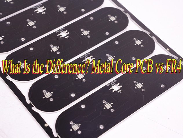
Which is difference between metal core PCBand FR4? This article compares the structural characteristics, thermal performance, and applicable scenarios of metal core and FR4 PCBs, providing accurate selection guidance.
A Metal Core PCB(MCPCB) is a printed circuit board with a metal base layer, typically aluminum or copper, designed for efficient heat dissipation in high-power applications. Its three-layer structure consists of copper circuitry, dielectric insulation, and metal core, enabling superior thermal management.
This makes it ideal for LED lighting, automotive electronics, and industrial power systems. The metal core acts as a heat sink, transferring heat away from components to prevent overheating while maintaining electrical insulation through the dielectric layer. This design ensures reliable performance in high-temperature environments.
What Is a FR4 PCB?
FR4 PCB is a printed circuit board made from FR-4 material, a flame-retardant glass fiber reinforced epoxy resin composite widely used in electronics due to its excellent mechanical strength, electrical insulation, and thermal stability.
It serves as a reliable substrate for mounting components while ensuring dimensional stability under varying environmental conditions. The material’s UL94 V-0 flammability rating and cost-effectiveness make it the standard choice for most consumer electronics, industrial equipment, and communication devices.
What Is the Difference? Metal Core PCB vs FR4
Material Composition & Structure
FR4 PCB: Manufactured from woven glass fiber impregnated with epoxy resin, this composite material offers insulation and mechanical strength. Its mature fabrication process supports multi-layer stacking for complex circuit designs, with copper traces plated on surfaces, ideal for standardized electronic module production.
Metal Core PCB: Built with aluminum or copper substrates in a “sandwich” architecture (circuit layer-insulation layer-metal base), the metal layer provides thermal support. Aluminum substrates are lightweight and cost-effective, while copper substrates deliver superior thermal conductivity (>380W/m·K). Insulation layers often use thermal silicone or ceramic-filled materials to balance electrical isolation and heat conduction.
Thermal Performance
FR4 PCB: Thermal conductivity ~0.3W/m·K, weak heat dissipation suitable for low-to-mid power applications. In LED modules or low-power supplies, external heatsinks are required to prevent thermal buildup that raises chip junction temperatures and shortens lifespan.
Metal Core PCB: Thermal conductivity ranges from 1-380W/m·K (aluminum: 1-3W/m·K, copper: >380W/m·K), achieving 6-9 times higher efficiency than FR4. For example, in automotive LED headlights, copper substrates rapidly dissipate heat from IGBTs, preventing light decay or burnout.
CTE Matching
FR4 PCB: Coefficient of Thermal Expansion (CTE) 12-24ppm/°C, significantly differing from copper’s 17ppm/°C, leading to delamination risks under thermal stress. Repeated thermal cycling may cause micro-cracks at FR4-copper interfaces, reducing electrical reliability.
Metal Core PCB: CTE closely matches copper (e.g., aluminum: 24ppm/°C), minimizing thermal cycling failure risks. The low CTE differential ensures stable electrical connections in high-reliability applications like aerospace or industrial control systems.
Mechanical Strength & Environmental Adaptability
FR4 PCB: Flexural strength ~480MPa, suitable for consumer electronics but prone to deformation under high temperature/pressure. While stable in everyday devices, it risks board fracture in vibration-heavy industrial environments.
Metal Core PCB: Metal substrates enhance rigidity, vibration/impact resistance, and suitability for extreme conditions like automotive electronics or industrial equipment. For instance, in new energy vehicle motor controllers, aluminum substrates withstand high-frequency vibrations and thermal shocks, ensuring circuit stability.
Electrical Performance
CDielectric constant 4.0-4.8, loss tangent 0.01-0.02, optimal for mid-to-low frequency signal transmission. Enables low-loss signal routing in communication devices, supporting high-frequency/high-speed designs.
Metal Core PCB: High-frequency performance depends on insulation layer design. While typically prioritized for thermal management, electrical performance slightly lags FR4. Optimized insulation materials (e.g., low-dielectric polymers) can balance high-frequency signal integrity with thermal efficiency.
Cost & Processing
FR4 PCB: Low cost, easy processing, and compatibility with complex multi-layer designs. Mass-produced by standard PCB factories at 1/3 to 1/5 the cost of metal core PCBs, ideal for large-scale consumer electronics.
Metal Core PCB: Higher costs due to specialized processing (e.g., metal substrate etching, precision drilling) and single/simple multi-layer structures. Despite elevated per-unit costs, long-term thermal management benefits reduce system maintenance expenses.
Application Scenarios
FR4 PCB: Dominates general-purpose fields like consumer electronics, communication devices, and home appliances (e.g., smartphone motherboards, router PCBs), leveraging low cost and mature processes for rapid iteration.
Metal Core PCB: Targets high-power, thermally demanding scenarios such as LED lighting, power modules, automotive electronics, and industrial equipment (e.g., streetlight drivers, EV battery management systems), optimizing thermal management to enhance device reliability.
Why Are Metal Core PCBs Better at Dissipating Heat than FR4 PCBs?
Reasons why MCPCB better at dissipating heat than FR4 PCB:
Direct Thermal Path via Metal Substrate: Aluminum/copper substrates in Metal Core PCBs create a vertical thermal channel from the chip through the insulating layer to the metal base. This bypasses FR4’s multi-layer dielectric thermal resistance stack-up, reducing thermal resistance by 60-90%. For example, in IGBT modules, copper-based PCBs can lower junction temperatures by 20-30°C, directly extending device lifespan.
Optimized Insulation Layer Materials: Metal Core PCBs use thermally conductive silicones, ceramic fillers (e.g., AlN), or nano-composites as insulating layers. These materials balance electrical isolation with high thermal conductivity (5-20W/m·K for AlN-filled layers vs. FR4’s 0.3W/m·K), creating a “thermal short-circuit” effect for rapid heat transfer.
Active Thermal Structure Design: Metal substrates can be machined with fins, thermal via arrays, or embedded heat pipes to actively expand surface area. In LED streetlights, aluminum substrates with radial fins increase heat dissipation area by 300%, enabling passive air cooling without additional fans.
Thermal-Mechanical Stability: Metal’s high rigidity minimizes thermal deformation impacts on circuits. In automotive power systems, aluminum substrates exhibit <0.1% warpage across -40°C to 125°C cycles, compared to FR4’s >0.5% deformation that risks solder joint fatigue.
System-Level Thermal Integration: Metal Core PCBs integrate directly with enclosures/heatsinks to form a unified thermal management chain. In 5G base station power modules, copper substrates bond with aluminum chassis for large-area passive cooling, reducing reliance on active cooling components and lowering system complexity/cost.
Why is Metal Core PCB More Suitable for High-Power Application Than FR4 PCB?
Superior Thermal Conductivity Materials
Metal core PCBs utilize copper (385 W/mK), aluminum (200 W/mK), or steel alloys with thermal conductivity 50-1000 times higher than FR4 (0.4 W/mK). This allows rapid heat dissipation from components, preventing thermal buildup-induced performance degradation or failure. For example, in 1000A automotive IGBT modules, copper substrates limit temperature rise to ≤30℃, while FR4 may trigger thermal protection due to localized overheating.
3D Heat Conduction Architecture
Thermal via arrays (0.1mm micro-vias at 100 holes/cm² density), embedded copper blocks (0.5-2mm thick), and metal backplate heat sinks form a tiered heat conduction path: component → thermal vias → substrate → external heatsink. This vertical heat transfer achieves 3-5 times higher efficiency than FR4’s planar heat spreading, ideal for high-power-density scenarios like LED streetlights and 5G base station PA modules.
Enhanced Heat Diffusion & Thermal Uniformity
High thermal diffusivity of metals (e.g., aluminum at 97 mm²/s) enables heat to spread evenly across the substrate within 0.1 seconds, avoiding localized hotspots that plague FR4 (thermal diffusivity: 0.3 mm²/s). During 150℃ thermal shock tests, metal core PCBs exhibit stable temperature profiles, whereas FR4 shows stepwise heating that risks component thermal stress cracking.
Low-Resistance Heat Dissipation Path
Direct contact between component pads and the metal substrate via high-conductivity solder (e.g., SnAgCu) achieves thermal resistance as low as 0.1℃/W—significantly lower than FR4’s insulation layer resistance (>10℃/W). This direct path minimizes interlayer thermal resistance accumulation, ensuring stable high-power operation.
Metal substrates withstand temperatures >300℃ (e.g., copper), while FR4 softens above 130℃, risking delamination or solder joint failure. Metal core PCBs pass 1000-hour 85℃/85%RH CAF (Conductive Anodic Filament) tests for corrosion resistance, outperforming FR4’s 500-hour limit and reducing long-term failure rates.
Extreme Environment Adaptability
In aerospace and deep-sea applications, metal core PCBs endure -55℃ to 125℃ temperature swings, high pressure, and salt spray without degradation. FR4, prone to moisture absorption and insulation breakdown, fails in such conditions—e.g., satellite power modules rely on steel alloy substrates for vacuum stability.
How Does Cost Difference between FR4 and Metal Core PCB?
The unit price of a standard double-sided FR4 PCB (1.6mm thickness) is approximately $2-$5 per piece. Leveraging a mature supply chain and the low-cost advantages of glass fiber substrates, it is suitable for large-scale mass production, with the unit price for an order of 10,000 pieces being reduced to $0.5 per piece. Metal core PCBs (MCPCBs) of the same size cost $15-$50 per piece, 7-10 times the cost of FR4.
This is mainly due to the high price of aluminum/copper core substrates (approximately $10-$30/㎡, 3-5 times the cost of FR4 substrates), the need for specialized surface treatment processes such as drilling and anodizing (which increase manufacturing costs by 30%-50%), and the difficulty in allocating processing losses in small-batch production, limiting the room for cost reduction.
How to Choose between Metal Core PCB and FR4 PCB?
Clarify Power Requirements & Thermal Constraints
High-power scenarios (≥50W/cm² heat density): Choose metal core PCB (aluminum/copper-based) for 6-9x higher thermal conductivity (1-380W/m·K vs. FR4’s 0.3W/m·K), preventing overheating in LED lighting, power modules, or automotive IGBTs.
Low-power scenarios (<20W/cm²): Optimize for FR4 due to lower cost and mature fabrication, ideal for consumer electronics and home appliances.
Evaluate Environmental Resilience
Extreme conditions (high temp/vibration/humidity): Metal core PCB’s rigid metal base (2-3x stronger than FR4) withstands shocks in automotive power systems or industrial drives.
Standard environments (indoor/low-vibration): FR4 suffices for basic mechanical strength in routers or phone motherboards.
Balance Cost & Long-Term Benefits
Budget-sensitive/mass production: FR4 wins with low material costs, complex multi-layer support, and quick scaling.
High reliability/longevity focus: Metal core PCB reduces secondary cooling costs (e.g., heat sinks/fans) and extends device life, justifying its higher unit cost in 5G power supplies.
Match Electrical & Signal Requirements
High-frequency applications (≥1GHz): FR4’s superior dielectric constant (4.0-4.8) and loss tangent (0.01-0.02) suit fine-line RF designs.
Thermal-priority scenarios (e.g., LED drivers): Metal core PCB balances heat dissipation with optimized insulators like thermal silicone.
Consider Thermal Expansion Compatibility
Frequent thermal cycling (outdoor/industrial control): Metal core’s CTE (e.g., aluminum: 24ppm/°C) aligns with copper traces (17ppm/°C), minimizing interface stress and delamination risk.
Stable thermal environments (indoor): FR4 works with stress-relief designs (e.g., thermal buffer layers) at lower cost.
Factor in Design Complexity & Manufacturability
Complex multi-layer/high-density interconnects: FR4’s mature processes support intricate stacking and fine-pitch routing.
Simple/single-layer thermal-centric designs: Metal core PCB’s streamlined structure reduces manufacturing complexity, ideal for cost-sensitive thermal applications.
Assess Sustainability & Recycling Potential
Eco-conscious projects: FR4’s glass-fiber/epoxy composition is recyclable via specialized processes, while metal core PCBs (aluminum/copper) offer higher material recovery rates, aligning with circular economy goals.
Why Choose EBest Circuit (Best Technology) as Your Metal Core PCB Manufacturer?
Mature Process Library & Parameterized Design Support: Leverage proven process libraries and parameterized design templates for single-layer to multi-layer metal-core substrates (aluminum/copper/iron-based), reducing trial-and-error costs by 30% and accelerating time-to-market for rapid iteration projects.
Dual Certification Compliance Guarantee: Meet stringent medical (ISO 13485) and automotive (IATF 16949) industry standards with dual certifications, shortening product launch cycles by 2-4 weeks and minimizing compliance risks for swift project validation.
24-Hour Rapid Prototyping Delivery: Enable same-day design validation closure and next-day physical prototype delivery for urgent needs, supporting fast design feasibility verification and market entry acceleration.
Full-Process 12-Step SPC Quality Control: Implement batch-specific CPK≥1.33 testing across thickness, thermal conductivity, and insulation resistance, ensuring ≥99.5% yield to minimize rework losses and provide reliable mass production assurance.
Transparent Tiered Pricing System: Eliminate hidden costs like mold/engineering fees, optimize metal material costs by 30% for bulk orders, and offer clear budgeting support for precise project cost management.
One-Stop Full-Process Service Chain: Cover end-to-end workflows from design support, prototyping, mass production, surface finishing (ENIG/OSP), to assembly testing, cutting multi-vendor coordination costs by 50% and freeing focus for core design optimization.
Free DFM Design Optimization: Proactively identify process risks (e.g., thermal stress, etching defects) to optimize layout and material selection, lowering production costs by 20% and enhancing manufacturability for seamless design-to-manufacturing transition.
Customized Thermal Management Solutions: Utilize high thermal conductivity materials (aluminum ≥2.0W/m·K, copper ≥380W/m·K) to design thermal vias, integrate heat sinks, and perform thermal simulations, ensuring ≤20℃ temperature rise in high-power scenarios for enhanced product reliability.
Welcome to contact us if you have any request for metal core PCBs: sales@bestpcbs.com.
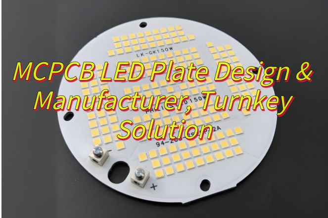
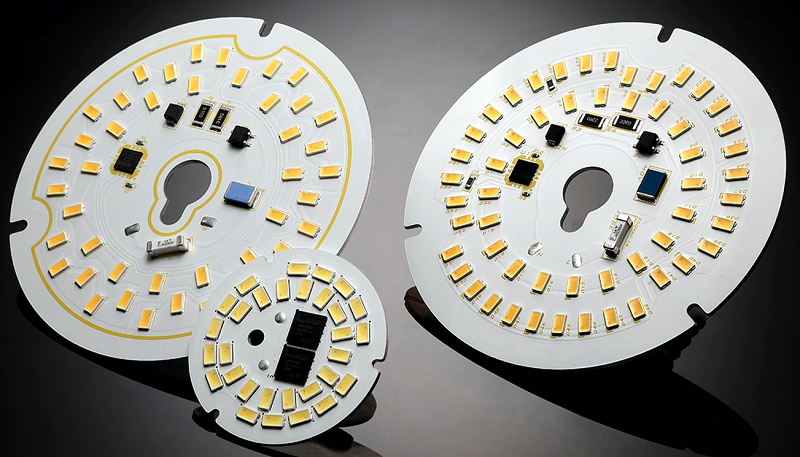
What isMCPCB LED plate? This guide explores its construction, applications, design principles, manufacturing, and cost factors for optimal thermal management solutions.
Are you worried about these problems?
Does your lamp lose 30% brightness after half a year of use?
Is the chip scrapped due to deformation of the substrate?
Does the micro-pitch LED below P1.0 have local overheating due to insufficient heat dissipation?
EBest Circuit (Best Technology) can provide solutions:
1.2W/m·K high thermal conductivity aluminum substrate + 5mil ceramic insulation layer, junction temperature reduced by 18℃, actual measured data, free thermal imaging testing service.
Nano-ceramic coating technology (thermal resistance <1.0K·cm²/W), supports 0.5mm pad spacing design, has passed 10,000 hours accelerated aging test.
Welcome to contact us if you have any request for metal core PCB: sales@bestpcbs.com.
What Is the Meaning of MCPCB LED Plate?
A MCPCB LED platerefers to a Metal Core Printed Circuit Board (MCPCB) specifically engineered for LED lighting applications. It features a metal base (typically aluminum or copper) as the core material, bonded with a thermally conductive dielectric layer and a copper circuit layer. Designed to efficiently dissipate heat generated by high-power LEDs, it ensures optimal performance, reliability, and longevity of LED modules, fixtures, or displays by preventing overheating. Commonly used in automotive lighting, streetlights, and high-brightness LED systems.
MCPCB LED PCB Construction
Metal Base Layer
Material: Aluminum (most common) or copper.
Function: Acts as a heat sink, drawing thermal energy away from LEDs to prevent overheating and extend component lifespan.
Dielectric Layer
Material: Thermally conductive epoxy or ceramic-filled prepreg.
Function: Electrically isolates the metal base from copper traces while enabling efficient heat transfer (thermal conductivity: 1–8 W/m·K).
Copper Circuit Layer
Thickness: 1–10 oz (35–350 µm).
Function: Transmits electrical signals and power to LEDs; thicker copper (≥2 oz) supports high-current applications (>3A per trace).
Solder Mask Layer
Material: Epoxy-based or polyimide coating.
Function: Protects copper traces from oxidation, solder bridging, and environmental contaminants (e.g., moisture, dust).
Surface Finish
Options: HASL (cost-effective), ENIG (flat surface for fine-pitch SMT), or OSP (organic solderability preservative).
Function: Ensures reliable solder joints during assembly and prevents corrosion.
How Does the MCPCB LED Plate Work?
Heat Generation: LEDs convert electrical energy into light, generating waste heat (typically 50–70% of input power).
Thermal Conduction: Heat transfers from LED junctions through solder joints to the copper circuit layer.
Dielectric Layer Transfer: The thermally conductive dielectric (epoxy/ceramic) rapidly channels heat from copper traces to the metal base.
Metal Base Dissipation: Aluminum/copper base acts as a heat sink, spreading heat across its surface area and radiating it into the environment.
Cooling Efficiency: Reduces LED junction temperature by 20–40% compared to FR4 PCBs, preventing lumen degradation and color shift.
Performance Impact: Maintains LED efficacy (>90% initial brightness) and lifespan (>50,000 hours) by avoiding thermal runaway.
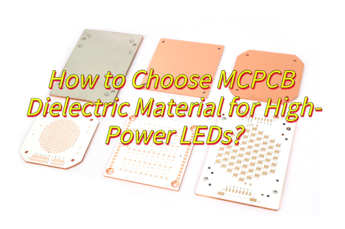
How to choose MCPCB dielectric materialfor high-power LEDs? This guide covers material functions, types, selection criteria, and design best practices for high-power LED applications.
Are you worried about these issues?
LED temperature is too high, causing accelerated light decay?
Uneven thickness of insulation layer causes short circuit risk?
Is it difficult to control the cost of small batch orders?
EBest Circuit (Best Technology) provide you with:
Free thermal analysis report:Dielectric layer thermal optimization plan is issued within 48 hours
Full process quality control: third-party test data is provided for each batch (including thermal conductivity/voltage resistance test)
Customized formula: adjust dielectric layer parameters according to power density (0.5-4.0W/m·K optional)
Welcome to contact us if you have any inquiry for MCPCB: sales@bestpcbs.com.
What Is MCPCB Dielectric Material?
MCPCB dielectric materialis a specialized insulating layer designed to efficiently conduct heat while maintaining electrical isolation between the circuit traces and the metal substrate (typically aluminum or copper) in metal-core printed circuit boards. Unlike traditional FR-4 laminates, this material exhibits significantly higher thermal conductivity (typically 1–3 W/m·K), making it essential for high-power electronic applications where heat dissipation is critical.
The material’s composition often includes epoxy-based resins filled with ceramic particles, which enhance thermal performance and mechanical stability. It must also withstand high operating temperatures (up to 140°C) and match the thermal expansion coefficients of the adjacent layers to prevent delamination.
What Are Functions of MCPCB Dielectric Materials?
Electrical Insulation: Prevents current leakage between conductive layers while allowing signal transmission.
Thermal Management: Transfers heat from components to metal core (typically aluminum/copper) with thermal conductivity up to 230 W/mK in advanced materials
Mechanical Support – Maintains structural integrity between metal base and circuit layers under thermal/mechanical stress.
Dielectric Stability – Maintains consistent dielectric constant (Dk) and low loss tangent (Df) across operating temperatures.
Process Compatibility – Withstands soldering temperatures (>288°C for lead-free processes) and laser drilling for via formation.
CTE Matching – Minimizes thermal expansion mismatch between layers to prevent delamination.
What Are Applications of MCPCB Dielectric Materials?
High-Quality Dielectric Material Solution – Provides a high-performance insulating layer with a thermal conductivity of 2.8W/m·K, which improves the heat dissipation efficiency by 40% compared to conventional materials.
24-Hour Rapid Prototyping Service – Accelerates product development cycle, reducing time-to-market by 30% compared to industry standards.
Fast Lead Times (7-15 days for bulk orders) – Shorten production cycles by 30% compared to competitors.
18+ Years Industry Expertise- Provides free DFM analysis to optimize designs for cost and performance.
Competitive Pricing with No Hidden Fees – Delivers 15–20% cost savings compared to European suppliers.
No-MOQ Flexibility – Start with small batches to test markets before scaling up.
Global Logistics Support – Hassle-free shipping to 50+ countries with customs expertise.
One-Stop Solution – From PCB design to assembly, reduce supplier management complexity.
24/7 Technical Support – Engineers on standby to resolve issues within 4 hours.
Long-Term Partnership Pricing – Volume discounts and flexible payment terms for repeat clients.
By integrating rapid response with professional technical services, we help customers achieve the core value of reducing R&D cycle by 50%+ and improving mass production yield to 99%, please feel free to contact EBest Circuit (Best Technology) if you have any request for MCPCB: sales@bestpcbs.com.
What is thermal substrates MCPCB? This guide explores its thermal properties, specifications, benefits, applications, material selection, design strategies, and supplier criteria for optimized thermal management.
Why do traditional PCBs always overheat and fail in high-power scenarios? How to balance heat dissipation performance and production costs? How to avoid thermal stress tearing in multi-layer complex designs?
EBest Circuit (Best Technology) Can Provide:
Precise thermal conductivity design – Customized metal stacking (copper/aluminum hybrid substrate) + high thermal conductivity insulation layer (8W/m·K), reducing temperature difference by 40%.
Cost-optimized architecture – Partitioned heat dissipation solution: copper in critical areas and aluminum in non-critical areas, saving 30%+ in costs.
Feel free to contact EBest Circuit (Best Technology) if you have any request for MCPCB: sales@bestpcbs.com.
What Is Thermal Substrates MCPCB?
Thermal Substrate MCPCB, short for Metal Core Printed Circuit Board, is a specialized type of printed circuit board designed primarily to enhance heat dissipation in electronic systems by integrating a thermally conductive metal base, such as aluminum or copper, which efficiently transfers heat away from mounted components to prevent overheating and ensure stability.
Its layered construction typically comprises a copper circuit layer for electrical routing, an insulating dielectric layer made from polymer materials filled with ceramics to balance electrical isolation and thermal conductivity, and the metal core that acts as a heat spreader, facilitating faster thermal transfer than standard alternatives.
Thermal Substrates MCPCB Specifications
Parameter Category
Typical Specification Range
Technical Notes
Metal Base Material
Aluminum (Al) / Copper (Cu)
Al base: 1.3-2.2 W/m·K thermal conductivity; Cu base: ~400 W/m·K (higher cost)
Copper Thickness: 1oz (35μm) for low power; ≥2oz (70μm+) for high current
Role: Thick copper reduces I²R losses, minimizing self-heating in traces.
What Are Advantages of Thermal Substrates PCB?
High-Efficiency Cooling – Metal base conducts heat 5-10x faster than standard PCBs, keeping components 30-50% cooler.
Enhanced Reliability – Reduces thermal stress, doubling or tripling the lifespan of LEDs, power semiconductors, and high-current devices.
Space-Saving Design – Built-in metal heatsink eliminates bulky external cooling systems, ideal for compact electronics like automotive modules.
High Current Handling – Supports thick copper traces (2oz+) to safely manage currents over 100A without overheating.
Dimensional Stability – Low thermal expansion minimizes warping, ensuring reliability in multi-layer or high-temperature environments.
What Are Applications of Thermal Substrates PCB?
High-Power LED Lighting – Ensures stable operation of COB/LED modules by dissipating heat directly through metal cores, preventing lumen depreciation.
Automotive Electronics – Critical for powertrains, ECUs, and battery management systems operating in high-temperature environments without active cooling.
Industrial Power Modules – Supports VFDs, motor drives, and inverters requiring efficient heat removal from IGBTs/MOSFETs under heavy loads.
Telecom Infrastructure – Enables compact RF amplifiers and base station components to handle high frequencies without thermal throttling.
Consumer Electronics – Used in gaming consoles, laptop chargers, and high-end audio amplifiers where space is limited but heat generation is high.
How to Choose the Material of Thermal Substrate MCPCB?
Thermal Substrate MCPCB Material Selection Guide
Power Density
High Power (>5W/cm²): Choose copper base (3-4W/m·K) for superior heat spreading.
Moderate Power: Aluminum base (1-2.5W/m·K) balances cost and performance.
Cost Sensitivity
Budget-Critical: Aluminum substrates cost 20-30% less than copper.
Performance-Priority: Copper justifies premium for extreme thermal demands.
Environmental Conditions
High Humidity/Corrosion Risk: Anodized aluminum or nickel-plated copper.
Extreme Heat (≥150℃): Copper with high-temp dielectric (e.g., polyimide).
Technical Expertise: Verify experience in high-power applications (e.g., LED, automotive, industrial). Ask for case studies showing thermal performance data.
Material & Process Control: Ensure suppliers use certified materials (e.g., ISO 9001 for dielectric layers) and have in-house thermal conductivity testing.
Prototyping Capability: Prioritize suppliers offering free/low-cost prototypes with thermal imaging reports to validate design feasibility.
Thermal Simulation Support: Choose suppliers providing CFD (Computational Fluid Dynamics) analysis to predict heat distribution before production.
Quality Assurance: Check for IPC-6012/6013 compliance and ask for third-party test reports (e.g., thermal resistance, dielectric breakdown).
Lead Time & Scalability: Confirm standard lead times (ideally ≤2 weeks for prototypes) and capacity to scale to 10K+ units monthly.
Cost Transparency: Request itemized quotes separating material, fabrication, and testing costs. Avoid suppliers with hidden tooling fees.
Post-Production Support: Ensure suppliers offer failure analysis and warranty coverage (minimum 1 year for thermal performance defects).
Welcome to contact EBest Circuit (Best Technology) if you have any request for MCPCB thermal solution: sales@bestpcbs.com.
Why choose 1 Layer MCPCB for outdoor solar cells? This guide explores its structure, thermal advantages, and reliability enhancements for harsh environments.
Solar Energy Innovators: Are you struggling with:
Heat-induced efficiency loss in outdoor solar arrays?
A 1 Layer MCPCB(Metal Core Printed Circuit Board) is a specialized circuit board featuring a single conductive copper layer bonded to a metal substrate, usually aluminum. The metal core efficiently transfers heat away from components, making it ideal for high-power applications where thermal management is essential.
The structure consists of three main parts: a metal base for heat dissipation, a dielectric layer for electrical insulation, and a single copper layer for circuitry. This design ensures effective cooling while maintaining electrical isolation. Though simpler than multi-layer boards, it offers excellent thermal performance for LED lighting, power electronics, and automotive systems.
With its straightforward layout, a 1 Layer MCPCB balances cost-effectiveness and reliability, making it a preferred choice for heat-sensitive electronics requiring durability and efficient thermal regulation.
How thick Is a 1 layer MCPCB?
Here’s a structured breakdown of typical thickness specifications for a 1 Layer MCPCB:
Metal Core Thickness
The base metal layer (usually aluminum) typically ranges from 1.0mm to 3.0mm, with 1.5mm and 2.0mm being most common for standard applications.
Thicker cores (e.g., 3.0mm+) may be used for extreme heat dissipation needs.
Dielectric Layer Thickness
The insulating layer between the metal core and copper ranges from 50µm to 150µm (0.05mm to 0.15mm).
Thinner dielectrics improve heat transfer but require precise manufacturing.
Copper Layer Thickness
The single conductive copper layer is commonly 1oz (35µm) or 2oz (70µm) but can go up to 3oz+ for high-current designs.
Overall Board Thickness
Total thickness typically falls between 1.2mm to 3.2mm, depending on the combined layers.
Example: A standard 1.5mm aluminum core + 100µm dielectric + 1oz copper ≈ 1.6mm total.
Customization Factors
Thickness can be adjusted based on thermal, mechanical, or electrical requirements.
Thinner boards suit compact designs, while thicker variants enhance rigidity and heat spreading.
What Is the Dielectric Layer of the 1 Layer MCPCB?
The dielectric layer in a 1 Layer MCPCB serves as the electrically insulating yet thermally conductive interface between the metal core and copper circuit layer. Here’s a structured breakdown of its characteristics:
Primary Function: Electrically isolates the copper circuitry from the metal base (typically aluminum) while efficiently transferring heat from components to the metal core.
Material Composition: Often consists of polymer-based composites (e.g., epoxy resins) filled with thermally conductive ceramics (alumina, boron nitride) to enhance heat dissipation.
Thermal Performance: Anisotropic microstructures in advanced dielectric layers can improve thermal diffusivity by optimizing filler connectivity, reducing thermal resistance in high-power applications.
Thickness Range: Typically measures 50–150µm (0.05–0.15mm), balancing electrical insulation and thermal transfer efficiency.
Impact on LED Performance: Inefficient dielectric layers may lead to higher junction temperatures in LEDs, reducing luminous output and efficiency.
High-Power LEDs – Directs heat away from LEDs, keeping them cool for brighter, longer-lasting light.
Power Electronics – Manages heat in devices like inverters or motor drivers, ensuring stable performance under heavy loads.
Automotive Systems – Withstands heat and vibrations in car lights or control units, even in tough conditions.
RF/Microwave Devices – Reduces overheating in radios or antennas, maintaining clear signal strength.
Solar Equipment – Keeps solar charge controllers or inverters efficient by handling sunlight-generated heat.
Industrial Sensors – Durable design for factory sensors exposed to heat, dust, or movement.
Compact Gadgets – Slim, heat-friendly boards for laptops or gaming devices with powerful chips.
Why Choose 1 Layer MCPCB for Outdoor Solar Cells?
Heat Dissipation: Metal core efficiently conducts heat away from solar cells, preventing overheating and maintaining optimal conversion efficiency even under direct sunlight.
Temperature Stability: Withstands outdoor temperature fluctuations, reducing thermal stress on components and ensuring consistent performance during day-night cycles.
Durability in Harsh Conditions: Resists moisture, dust, and UV exposure, making it suitable for long-term outdoor use without degradation.
Cost-Effective Design: Simpler structure lowers production costs while still delivering reliable thermal management for solar applications.
Enhanced Lifespan: By keeping components cooler, it reduces wear and tear, extending the operational life of solar charging systems or inverters.
How to Enhance 1 Layer MCPCB Heat Dissipation to Extend Outdoor Solar Cells Lifespan?
Choose High-Conductivity Substrates: Use copper (385 W/m·K) for the metal core if weight allows. For lighter builds, select 1.5mm+ thick aluminum (237 W/m·K) with a matte finish to boost radiative cooling under sunlight.
Use Advanced Dielectric Materials: Replace standard epoxy with ceramic-filled polyimide (1.5–3 W/m·K) in the insulating layer. This cuts thermal resistance by 40–60%, accelerating heat transfer to the substrate.
Maximize Thermal Via Efficiency: Drill 0.3mm copper-plated vias beneath heat-generating components (e.g., diodes, MPPT chips) at 1mm spacing. Arrange vias in a grid pattern to create vertical heat pathways.
Integrate Passive Cooling Elements: Attach finned aluminum heat sinks (10–20mm tall) to the MCPCB’s backside. In compact spaces, use graphite sheets (1,500 W/m·K) or vapor chambers to spread heat evenly across the substrate.
Apply Emissivity-Enhancing Coatings: Coat the metal core’s exterior with black ceramic paint (emissivity >0.85). This increases infrared radiation, helping the board shed heat faster under direct solar exposure.
Optimize Component Layout: Place high-power components (e.g., transistors) away from solar cell active zones. Use thermal gap pads (2–4W/m·K) to ensure direct contact between parts and the MCPCB surface.
Validate with Thermal Modeling: Use ANSYS Icepak or similar tools to simulate heat flow. Adjust via patterns, material thickness, or component positions based on hotspot analysis (e.g., reduce via spacing in 50°C+ zones).
How to Improve 1-Layer MCPCB Reliability for Outdoor Solar Cells?
Select Durable Materials
Use aluminum (lightweight, corrosion-resistant) or copper (high conductivity) for the metal core. Pair with polyimide or modified epoxy dielectric layers to resist moisture and delamination while ensuring efficient heat transfer.
Boost Thermal Performance
Increase thermal via density under high-heat components (e.g., solar charge controllers) to direct heat to the metal base. Thicken the substrate (e.g., 2mm aluminum) or add external heat sinks for passive cooling, reducing active system reliance.
Apply Protective Coatings
Coat circuits with UV-resistant, waterproof conformal coatings (e.g., silicone for coastal areas) to shield solder joints and traces from humidity, dust, and salt spray.
Use Robust Components
Choose outdoor-rated parts (e.g., capacitors rated for -40°C to 125°C) and high-reliability solder (e.g., SAC305).
Strengthen Design and Test
Match dielectric layer CTE to metal and copper traces to prevent cracking. Secure edges with epoxy or fasteners for vibration resistance. Validate with 1,000+ hours of 85°C/85%RH damp heat, thermal shock (-40°C to 125°C), and salt-spray tests.
How to Enhance 1-layer MCPCB Durability for Harsh Outdoor Conditions?
Use Corrosion-Resistant Substrates
Select anodized aluminum (5052 alloy) for coastal or industrial areas. Anodizing creates a 5–25µm oxide layer that resists salt and moisture. In extreme corrosion environments, choose 316 stainless steel despite its higher weight.
Apply Multi-Layer Protective Coatings
Coat circuits with a 50–100µm silicone-based layer (e.g., Dow Corning 1-2577) to block moisture and dust. Add a 20–30µm acrylic topcoat for scratch resistance, focusing on solder joints and exposed traces.
Reinforce Mechanical Stability
Thicken the dielectric layer to 100µm polyimide to reduce flexing under thermal stress. Secure board edges with epoxy adhesive or aluminum brackets to prevent warping from temperature swings (-40°C to 125°C) or vibration.
Choose Outdoor-Rated Components
Use IP67-rated capacitors, resistors, and connectors with a -40°C to 125°C operating range. Select gold-plated contacts for connectors to resist tarnishing in humid environments.
Match Thermal Expansion Properties
Select dielectric layers with a coefficient of thermal expansion (CTE) close to aluminum (23–24 ppm/°C). Ceramic-filled polyimide (CTE 12–18 ppm/°C) reduces stress on copper traces during temperature fluctuations.
Validate with Accelerated Aging
Perform 2,000-hour thermal cycling (-40°C to 125°C, 1-hour dwells) and 96-hour salt-spray tests (ASTM B117). Include UV exposure (ISO 4892-3) to confirm coating integrity under prolonged sunlight.
Conclusion
In summary, 1 layer MCPCBs provide an efficient thermal management solution for outdoor solar cells with their optimized metal core structure, dielectric layer design, and enhanced durability features. By improving heat dissipation through material selection and layout optimization, these boards significantly extend solar cell lifespan while withstanding harsh environmental conditions. For projects requiring fast turnaround and reliable performance, our customized 1-layer MCPCB solutions offer the perfect balance of cost-effectiveness and thermal efficiency. Contact us today for a competitive quote: sales@bestpcbs.com.
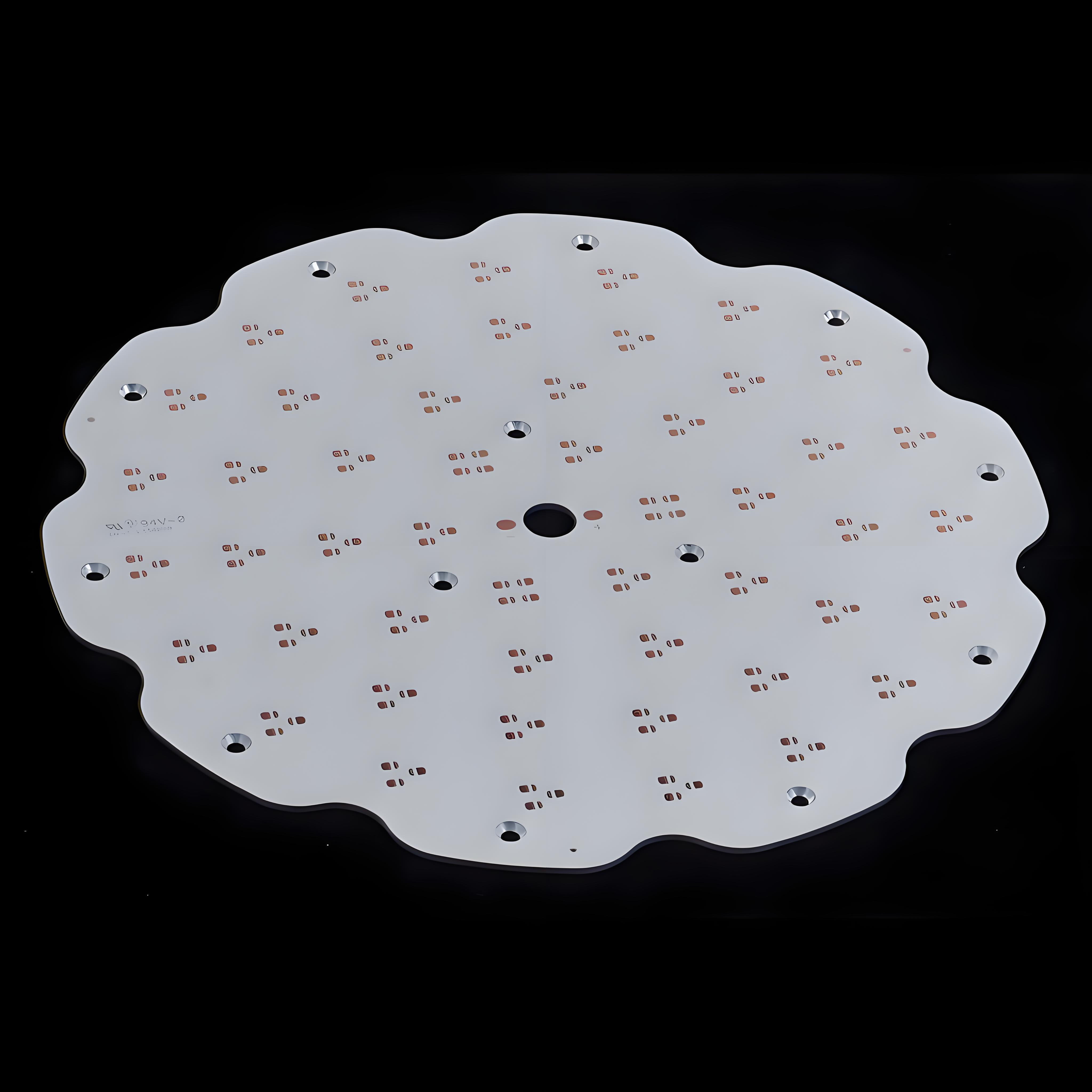
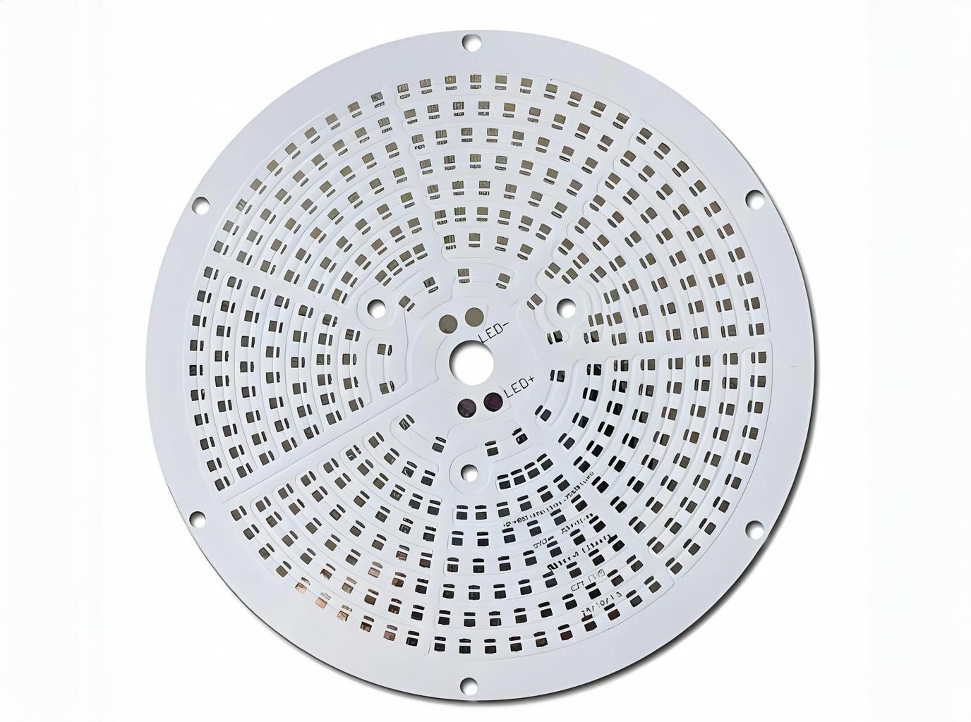
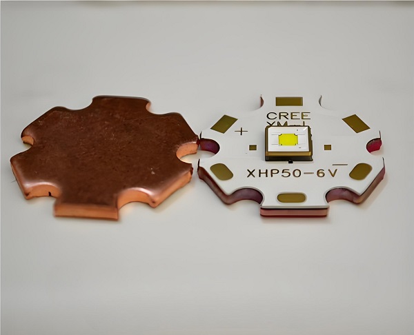
A sinkpad copper based PCB, also known as SinkPAD board or thermoelectric copper separation copper based PCB, is a specialized type of metal core printed circuit board. It mainly consists of two major parts: the top trace layer and the copper core/substrate. The top trace layer contains the electrical traces for the circuit, while the copper core serves as a heatsink.
A 1 – Layer SinkPAD board, a common type, consists of a copper circuit layer, a dielectric (non – conducting) layer, and a metal core/pedestal which is usually copper. It belongs to single – sided SinkPAD PCB and DTP (Direct Thermal Path) board, and is the most popular and cost – effective stack – up option with the fastest lead time.
Why Use Sinkpad Copper Based PCB?
Sinkpad copper based PCBs are used for several important reasons. After lamination, the electronics connection is on the trace layer, and the direct thermal conducting PAD comes from the copper core. The trace PAD on the trace layer is in the sink area of the copper core, which gives it the name “SinkPAD board”. This design allows for efficient thermoelectric separation.
These PCBs can reach a thermal conductivity of 400W/m.K. This high thermal conductivity is crucial in applications where heat dissipation is a major concern, such as in high – power LED lighting, power electronics, and other electronic devices that generate a significant amount of heat. By effectively dissipating heat, sinkpad copper based PCBs can improve the performance and reliability of electronic components and extend their lifespan.
Factors Affect the Price of Sinkpad MCPCB
Material type (aluminum vs. copper)
The choice of material has a significant impact on the price of sinkpad MCPCB. Copper is generally more expensive than aluminum. Copper has excellent thermal conductivity, which is one of the key advantages for sinkpad PCBs as it helps in better heat dissipation. However, the higher cost of copper raw materials and the more complex processing requirements contribute to the increased price.
Aluminum, on the other hand, is a more cost – effective option. It has relatively good thermal conductivity and is lighter in weight. But its thermal performance is not as good as copper. When the application requires high – end thermal performance, copper is often the preferred choice, but it comes at a higher price.
Board size and thickness
The size and thickness of the sinkpad copper based PCB also play a role in determining the price. Larger boards require more raw materials, such as copper and dielectric materials. Additionally, the manufacturing process for larger boards may be more complex, as it requires more precise alignment and processing steps.
Thicker boards also add to the cost. Thicker copper cores or additional layers of materials increase the material cost. Moreover, thicker boards may require more advanced manufacturing techniques to ensure proper electrical and thermal performance, which can drive up the production cost.
Layer structure
The layer structure of the sinkpad PCB is another important factor. A more complex layer structure, such as multi – layer sinkpad PCBs, is more expensive than single – layer ones. Multi – layer PCBs require more manufacturing steps, including additional lamination processes, drilling for vias to connect different layers, and more precise alignment of the layers.
Each additional layer adds to the complexity and cost of the manufacturing process. For example, a 1 – Layer SinkPAD board is the simplest and most cost – effective option, while a PCB with multiple trace layers and copper core layers will be significantly more expensive.
Order quantity
Order quantity has a direct impact on the price of sinkpad copper based PCBs. When the order quantity is large, the per – unit cost usually decreases. This is because manufacturers can take advantage of economies of scale. They can purchase raw materials in bulk at a lower cost, optimize their production processes, and reduce setup costs per unit.
For small – quantity orders, the fixed costs associated with setting up the production line, such as tooling costs and programming costs, are spread over a smaller number of units. As a result, the per – unit price is higher. So, customers who need a large number of sinkpad PCBs can often negotiate a better price per unit.
Custom thermal pad design
Custom thermal pad designs can also increase the price of sinkpad copper based PCBs. Standard thermal pad designs are more cost – effective because they can be produced using existing manufacturing processes and tools. However, if a customer requires a custom thermal pad design, it may involve additional engineering work, such as designing new masks, adjusting the manufacturing process, and conducting additional testing.
Custom designs may also require special materials or manufacturing techniques to meet the specific thermal requirements. All these additional steps and requirements add to the overall cost of the PCB.
Sinkpad Copper Based PCB Applications
Sinkpad copper based PCBs have several common uses in the electronics industry:
Thermoelectric separation applications:
Since the trace layer of SinkPAD boards is usually on the top side, they belong to single – sided SinkPAD PCBs and Direct Thermal Path (DTP) boards. This makes them suitable for applications where thermoelectric separation is required. For example, the SinkPad board provides excellent heat transfer from the LED to the base metal (copper) plate while maintaining excellent electrical isolation.
High – power LED applications:
1 – Layer copper base SinkPad PCB: It can be used with surface mount and chip & wire components. The thermal PAD of the LED touches the convexity of the copper core/pedestal directly, achieving a thermal conductivity of 400W/m.K. The pad of the LED touches the copper base directly, allowing the heat generated by the LED to be dissipated quickly into the air or a heatsink, achieving the best heat dissipation and conduction.
2 – Layers copper base SinkPad PCB: It can also be used with surface mount and chip & wire components. Similar to the 1 – layer version, the thermal PAD of the LED touches the convexity of the copper core/pedestal directly, with a thermal conductivity of 400W/m.K.
In general, sinkpad copper based PCBs are used to provide superior thermal performance for medium – to high – power LEDs and other chips/components.
How Does A SinkPAD board Differ From A Traditional PCB?
A SinkPAD board is a special type of metal core PCB. In a SinkPAD board, the thermal conductive PAD is the convexity area of the copper core/pedestal, allowing the thermal PAD of the LED to touch the convexity area of the metal core directly. This enables the heat of the LED to be dissipated into the air much faster and more efficiently than a conventional PCB.
The SinkPad provides excellent heat transfer from the LED to the metal base plate/pedestal while maintaining excellent electrical isolation. The base copper base gives the board substrate mechanical integrity, distributes and transfers the heat to a heat sink, mounting surface, or directly to the ambient air.
In contrast, traditional PCBs do not have this direct thermal path feature. The heating of the LED in a SinkPAD board conducts directly into the copper core, which is different from the traditional thermal path. Due to this, a SinkPAD board can offer superior thermal performance for medium – to high – power LEDs or other chips/components.
How to Design a SinkPAD Board?
When designing a SinkPAD board, the following points need attention:
1. Panel layout design
If the board outline is not square or rectangle, the outline has to be made via CNC routing or Die – punching. While designing the panel layout, at least 2mm space between the edge of the SinkPAD board (SinkPAD PCB) should be kept in order for routing or Die – punching.
2. Routing and punching
Several layers of SinkPAD PCB will be routed together to save time. But for punching, there is only one layer of SinkPAD board (SinkPAD PCB) each time. Die – punching will be used only when there are big volume orders as the cost of die – punching tooling is higher compared with other ways.
Moreover, in the lamination process (laminate & align board before hot process lamination), after specific steps, the electronics connection will be on the trace layer and the direct thermal conducting PAD comes from the copper core. The trace PAD on the trace layer seems in the sink area of the copper core, which is how the SinkPAD board gets its name. And because the electronic – related function is on the trace layer and thermal conduction is on the copper core, they are separated from each other, so it is also named a Thermoelectric separation circuit board.
Your Trust Sinkpad PCB Supplier – EBest Circuit (Best Technology)
EBest Circuit (Best Technology) is a reliable supplier of sinkpad PCBs. We offer high – quality SinkPAD boards with excellent thermal performance. Our products are designed and manufactured using advanced techniques to ensure precise separation of the copper core and trace layers, resulting in efficient thermoelectric separation.
EBest Circuit (Best Technology) can provide various types of sinkpad PCBs, including 1 Layer SinkPAD boards, 2 layers sinkpad MCPCB and multi-layer sinkpad MCPCB, to meet different customer requirements. We also have the ability to handle custom designs, whether it’s a custom thermal pad design or a specific layer structure. With their expertise and experience in the field, customers can trust EBest Circuit (Best Technology) to deliver high – quality sinkpad copper based PCBs at a reasonable price.
Frequently Asked Questions
1. What is a double – sided SinkPAD board?
A double – sided SinkPAD board consists of at least one layer of circuit layer on both the top and bottom sides of the SinkPAD board, a dielectric (non – conducting) layer, and a metal core/pedestal which is normally copper. More components can be placed on this type of board, but engineers need to consider heat conduction.
2. What are the components of a 1 – layer SinkPAD board?
A 1 – layer SinkPAD board consists of a copper circuit layer, a dielectric (non – conducting) layer, and a metal core/pedestal which is usually copper. It belongs to single – sided SinkPAD PCB and DTP board and is the most popular and cost – effective option with the fastest lead time.
3. How is a 2 – layer SinkPAD board different from a 1 – layer one?
A 2 – layer SinkPAD board has two layers of circuit layer on the same side, along with a dielectric layer and a copper metal core/pedestal. It also belongs to single – sided SinkPAD PCB and DTP board. The main difference is that more traces can be placed on a 2 – layer SinkPAD board compared to a 1 – layer one.
4. What defines a multi – layer SinkPAD board?
Multi – layer SinkPAD refers to a metal core board that has more than 2 layers of trace circuits, either on the same side or on both the top and bottom sides, and has a direct thermal path (PAD). Examples include 4L SinkPAD board or 4L SinkPAD double – sided board.
5. What is the first step in the SinkPAD board manufacturing process?
The first step in the SinkPAD board manufacturing process is to prepare the manufacturing files. This involves separating the copper core and trace from one Gerber layer into two different layers. One layer will have only the trace without the center heatsink PAD of the LED (trace layer), and the other layer will have only the heatsink PAD (copper core layer).
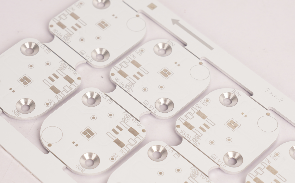
Metal core PCB is designed for applications requiring efficient heat dissipation, making it ideal for high-power electronics. Unlike standard PCBs, it features a metal base, typically aluminum or copper, that enhances thermal conductivity and improves durability. This design helps prevent overheating, ensuring stable performance in LED lighting, automotive systems, and power electronics. As industries demand reliable and heat-resistant circuit boards, metal core PCBs have become a preferred choice.
EBest Circuit (Best Technology) has over 18 years of experience designing metal core PCBs. We are a professional metal core PCB manufacturer, mainly involved in all types of PCB manufacturing. If you need a metal core PCB, please feel free to contact us at sales@bestpcbs.com.
What is a Metal Core PCB?
A metal core PCB (MCPCB) is a specialized type of printed circuit board that features a metal core instead of the standard FR4 or other non-metallic substrates. The metal core, typically made of aluminum, copper, or steel, helps dissipate heat efficiently, making it a preferred choice for high-power applications such as LED lighting, automotive electronics, and power conversion systems.
Unlike regular PCBs, which rely on thermal vias or external heat sinks for cooling, MCPCBs conduct heat directly through their metal base. This results in better thermal management, increased reliability, and a longer lifespan for electronic components. If you’ve ever wondered why some circuit boards perform better under high temperatures, chances are they are using metal core PCB technology.
What Are the Different Types of Metal Core PCBs?
Metal Core PCBs (MCPCBs) are classified based on three key dimensions: Layer Structure, Heat Dissipation, Application-Specific Features.
1. Classification by Layer Structure
Single-Layer MCPCB
Structure: A metal base, an insulating dielectric layer, and a single copper layer for circuit traces.
Best For: LED lighting, power supplies, and basic thermal management applications.
Key Benefit: Simple and cost-effective with efficient heat dissipation.
Two-Layer MCPCB
Structure: Two copper layers put on the one side of MCPCB, with an aluminum or copper base.
Best For: Power circuits requiring more routing flexibility than single-layer MCPCBs.
Key Benefit: Improved circuit complexity and higher current capacity.
Double-Sided MCPCB
Structure: Copper layers on both sides of the metal core, connected via plated through-holes (PTHs).
Best For: Automotive control systems, industrial power converters, and motor drivers.
Key Benefit: Enhanced circuit routing options and improved electrical performance.
Multilayer MCPCB
Structure: Multiple copper and dielectric layers stacked on a metal core.
Best For: Advanced applications like aerospace, telecommunications, and high-power LED lighting.
Key Benefit: Increased circuit density, better signal integrity, and superior heat dissipation.
2. Classification by Heat Dissipation Technology
Standard MCPCB
Structure: A conventional metal core PCB with a dielectric layer that transfers heat from components to the metal base.
Key Benefit: Moderate thermal performance, widely used in consumer electronics and LED modules.
SinkPAD MCPCB (Enhanced Thermal Management)
SinkPAD is a specialized MCPCB technology designed for superior heat dissipation by reducing thermal resistance. Unlike standard MCPCBs, SinkPAD boards allow heat to transfer directly from the component to the metal base without passing through an insulating dielectric layer.
1L SinkPAD Board (Single-Layer SinkPAD)
Structure: A single copper layer with direct thermal pathways to the metal core.
Best For: High-power LED modules and power supplies requiring fast heat dissipation.
Key Benefit: More efficient cooling than standard single-layer MCPCBs.
2L SinkPAD Board (Two-Layer SinkPAD)
Structure: Two copper layers with a thermal connection to the metal core.
Best For: Medium-power applications, such as LED drivers and automotive lighting.
Key Benefit: Improved thermal performance and better electrical conductivity.
Double-Sided SinkPAD Board
Structure: Copper layers on both sides of the metal core, providing heat dissipation pathways on both surfaces.
Best For: High-power industrial electronics, automotive systems, and power management circuits.
Key Benefit: Balanced thermal performance and high electrical efficiency.
Multi-Layer SinkPAD Board
Structure: Multiple copper layers with direct heat dissipation channels integrated into the metal core.
Best For: Aerospace, military, and high-end LED applications requiring extreme heat management.
Key Benefit: Maximized thermal efficiency for complex, high-power circuits.
3. Classification by Application-Specific Features
COB (Chip-on-Board) MCPCB
Structure: LED chips are mounted directly onto the metal core PCB without individual packaging.
Best For: High-brightness LED applications such as streetlights, automotive headlights, and stadium lighting.
Key Benefit: Lower thermal resistance, higher efficiency, and reduced size compared to traditional LED modules.
Selecting the right MCPCB depends on your thermal management needs, power requirements, and circuit complexity. For simple applications, a single-layer MCPCB may suffice, while high-power and heat-sensitive applications benefit from SinkPAD or multilayer MCPCBs.
What Materials Are Used to Make Metal Core PCBs?
MCPCBs are made from a combination of conductive and non-conductive materials to ensure durability and heat dissipation. Here’s a breakdown of the materials:
Metal Core – The base material is typically aluminum, copper, or stainless steel. Aluminum core PCBs are lightweight and cost-effective, while copper metal core PCBs offer superior heat dissipation but are more expensive.
Dielectric Layer – This electrically insulating but thermally conductive layer separates the copper circuit layer from the metal core. It plays a crucial role in transferring heat while preventing electrical shorts.
Copper Layer – The conductive layer where circuit traces are formed. The thickness of this layer varies based on current-carrying requirements, with heavy copper PCBs featuring thicker traces for power electronics.
The selection of metal core PCB materials depends on your design needs, thermal requirements, and budget.
How to Design a Metal Core PCB?
Designing a metal core PCB (MCPCB) requires meticulous planning to ensure optimal performance. Here are some key considerations for designing an effective MCPCB:
Component Placement
High-Power Components Near the Metal Core: Position high-power components close to the metal core to enhance heat dissipation and maintain thermal stability.
Thermal Management
Thermal Vias: Incorporate thermal vias to efficiently transfer heat from the components to the metal core.
Proper Spacing: Ensure adequate spacing between components to prevent overheating and maintain air circulation for effective cooling.
Layer Stack-up
Bonding Strength: When designing multilayer MCPCBs, ensure robust bonding between the dielectric and metal layers to maintain structural integrity and thermal conductivity.
Trace Width and Spacing
Wider Traces for Current Flow: Use wider traces to reduce resistance and improve current flow, especially for high-power applications.
Adequate Spacing for Safety: Maintain sufficient spacing between traces to prevent electrical shorts and ensure safety.
Drilling and Routing
Special Manufacturing Techniques: Due to the hardness of metal core boards, special drilling and routing techniques are required. Consult with your manufacturer to ensure compatibility with their production processes.
Design Software
Professional PCB Design Software: Utilize professional PCB design software to optimize the manufacturing process, prevent design flaws, and ensure compliance with industry standards.
Additionally, consider the following for a comprehensive MCPCB design:
Material Selection: Choose the appropriate metal core material (e.g., aluminum, copper) based on your thermal and mechanical requirements.
Dielectric Layer Properties: Select a dielectric layer with good thermal conductivity and electrical insulation properties.
Antipad Application: In double-sided MCPCB designs, apply an antipad to indicate the via-hole region that requires an insulating filter to prevent electrical shorts.
Superior Heat Dissipation: The metal core (e.g., aluminum or copper) rapidly absorbs and distributes heat away from components, reducing thermal stress and preventing performance degradation in high-power circuits.
Higher Durability: MCPCBs withstand extreme temperatures, mechanical shocks, and vibrations better than FR4, making them ideal for harsh industrial or automotive environments.
Improved Electrical Performance: Lower thermal resistance minimizes voltage drops and parasitic inductance, enhancing efficiency in high-current applications.
Extended Lifespan: Effective thermal management reduces component fatigue, significantly prolonging the operational life of electronics.
Compact Design: Eliminates the need for bulky heat sinks, enabling slim and lightweight solutions for space-constrained applications like LED modules or EV power systems.
What Are the Applications of Metal Core PCBs?
Thanks to their high thermal conductivity and reliability, MCPCBs are widely used in:
LED Lighting: Critical for high-brightness LED applications (e.g., streetlights, automotive headlights), where they prevent overheating and ensure consistent light output and longevity.
Automotive Electronics: Used in electric vehicle (EV) battery management systems, motor controllers, and brake systems to handle high currents and extreme temperature fluctuations.
Power Electronics: Essential for inverters, converters, and industrial power supplies that require heavy copper layers and stable thermal performance.
Medical Devices: Found in MRI machines, X-ray equipment, and surgical tools, where reliability and heat dissipation are critical for patient safety.
Telecommunications: Supports high-frequency RF/microwave circuits in 5G infrastructure and radar systems, reducing signal loss caused by heat buildup.
Why Choose EBest Circuit (Best Technology) as Your Metal Core PCB Manufacturer?
With so many circuit board manufacturing companies out there, why should you choose EBest Circuit (Best Technology)? Here’s what sets us apart:
18+ Years of Experience: We specialize in metal core PCB fabrication with cutting-edge technology over 18 years.
Wide Range of Solutions: From single-layer MCPCB to multi-layer SinkPAD board, we manufacture all types of PCBs. If you have related inquiries or questions, you are warmly welcome to contact us.
Custom Designs: Do you need a metal core PCB prototype? We offer quick-turn prototypes tailored to your needs.
High-Quality Standards: We use premium metal core PCB materials for better durability and performance.
FAQs of Metal Core PCB
1. What metals are in circuit boards?
Circuit boards contain different metals depending on their type. Copper is the most common metal used for conductive traces due to its excellent electrical properties. In metal core PCBs (MCPCBs), the core is typically made of aluminum or copper to improve heat dissipation. Steel is rarely used because it’s heavier and less effective at conducting heat.
2. What is the difference between FR4 and MCPCB?
MCPCB VS Regular PCB: What are Differences? FR4 PCBs are made from fiberglass-reinforced epoxy, offering a low-cost, durable, and electrically insulating solution. However, they have limited heat dissipation capabilities, making them suitable for applications with moderate power levels.
MCPCBs (Metal Core PCBs) have a metal base (usually aluminum or copper) with a thermally conductive dielectric layer, allowing them to dissipate heat 5–8 times better than FR4. These are ideal for high-power applications, such as LED lighting and power electronics, where heat management is critical.
3. How are metal core PCBs laminated?
Laminating a metal core PCB involves several steps:
Metal Base Preparation – The aluminum or copper core is cleaned and sometimes treated to improve insulation and corrosion resistance.
Dielectric Layer Application – A thermally conductive but electrically insulating layer is applied between the metal base and the copper circuitry.
Copper Lamination – The copper foil is bonded to the dielectric layer using high pressure and heat to ensure strong adhesion.
This process ensures the PCB can effectively transfer heat away from components while maintaining electrical insulation.
4. How to make metal core PCB?
The manufacturing process for metal core PCBs includes:
Cutting and Cleaning the Metal Core – The aluminum or copper base is cut to the required size and cleaned to remove any impurities.
Applying the Dielectric Layer – A heat-conductive but non-conductive layer is added to separate the metal core from the copper circuit.
Etching the Circuit Pattern – The copper layer is coated with a photoresist, exposed to UV light, and etched to create circuit traces.
Drilling and Plating – Holes are drilled for vias and plated with copper to establish electrical connections.
Surface Finishing – A protective finish like ENIG (Electroless Nickel/Immersion Gold) or OSP (Organic Solderability Preservative) is applied to prevent oxidation and improve solderability.
Testing and Quality Control – The finished boards undergo electrical and thermal testing to ensure they meet performance requirements.
This process results in a highly durable and heat-efficient PCB, making it suitable for applications that require superior thermal management.
In conclusion, metal core PCBs are the go-to solution for applications that demand superior thermal management, durability, and high performance. Whether you’re working with high-power LED lighting, automotive electronics, or power conversion systems, MCPCBs ensure stable operation under extreme conditions. With different types such as single layer MCPCB, multi layers MCPC, and advanced SinkPAD MCPCBs, designers can choose the right configuration based on their specific thermal and electrical requirements.
At EBest Circuit (Best Technology), we leverage 18+ years of experience in PCB manufacturing to deliver high-quality metal core PCBs tailored to your needs. From prototype development to mass production, we provide reliable, high-performance solutions with strict quality control. For inquiries or more info about metal core PCB, welcome to email us at sales@bestpcbs.com.
LED PCB Board Design is essential for creating efficient and durable LED lighting solutions. Whether for consumer electronics, automotive applications, or industrial lighting, a well-designed LED Light PCB Circuit Design ensures optimal performance and longevity. With the right PCB Design Service, you can achieve improved heat dissipation, electrical efficiency, and seamless integration of LEDs onto circuit boards. This led pcb design guide will walk you through everything you need to know about LED PCB design, from materials and circuit design to mounting methods and cost considerations.
What is an LED PCB Board?
An LED PCB board is a printed circuit board (PCB) specifically designed to support and power light-emitting diodes (LEDs). Unlike standard PCBs, LED PCBs focus on thermal management since LEDs generate heat, which, if not managed properly, can reduce efficiency and lifespan. Common applications of LED PCB boards include:
LED lighting strips for residential and commercial use
Automotive headlights and dashboards
Medical equipment displays
Smartphones, TVs, and digital billboards
A well-planned LED PCB design ensures even light distribution, durability, and energy efficiency.
What Materials Are Used in LED PCB?
Choosing the right material is crucial for LED PCB circuit design, as it directly affects heat dissipation, durability, and cost. The most commonly used materials are:
1. Aluminum Core PCB
The best choice for high-power LED PCB design
Features a metal core that dissipates heat efficiently
Commonly used in LED strip PCB design and automotive lighting
2. FR-4 (Fiberglass) PCB
A cost-effective choice but requires additional heat dissipation measures
Used in low-power LED applications
3. Ceramic PCB
Offers superior thermal conductivity
Used in high-end LED lighting applications requiring maximum heat resistance
Selecting the right material ensures that LED boards operate efficiently without overheating.
How to Make LED PCB Design?
When working on PCB design for LED light applications, especially for high power LED PCB design, it’s crucial to focus on efficient thermal management and optimized circuit layout to ensure longevity and performance. Proper LED PCB circuit design involves strategic LED placement, adequate heat dissipation, and careful component selection. Specifically, creating a simple LED PCB design involves several key steps:
1. Schematic Design
Use LED PCB design software like Altium Designer, Eagle PCB, or KiCad to create the electrical layout, including:
LED placement
Resistor and capacitor positioning
Power supply routing
2. PCB Layout
Optimize trace width and routing for efficient current flow
Use wide copper traces to prevent overheating
Implement thermal vias for heat dissipation
3. Simulation & Prototyping
Before manufacturing, test the PCB LED design using simulation software to detect issues early.
How to Build a Basic LED Circuit?
A basic LED circuit consists of:
LEDs (Light-emitting diodes)
A power source (battery or DC supply)
Resistors (to limit current and prevent damage)
Wires or PCB traces (to connect components)
Simple LED PCB Design Example
Step 1: Connect the LED anode (+) to the power supply via a resistor.
Step 2: Connect the LED cathode (-) to the ground.
Step 3: Ensure the resistor value matches the LED voltage and current ratings.
This simple circuit is the foundation of LED matrix PCB design, LED driver PCB design, and more.
What is the Width of LED PCB?
The width (thickness) of an LED PCB board depends on its application:
Standard LED PCBs: 1.6mm (most common for general applications)
High-power LED PCBs: 2.0mm – 3.2mm (for better heat dissipation)
Flexible LED PCBs: 0.2mm – 1.0mm (used in LED strips)
The correct PCB width prevents overheating and ensures mechanical stability.
How Do You Mount LEDs on a PCB?
LEDs can be mounted on PCBs using different methods, depending on the design and application:
1. Surface Mount Technology (SMT) – Best for SMD LED PCB Design
Uses solder paste and reflow soldering
Ideal for compact LED light PCB design
2. Through-Hole Technology (THT) – Used for High-Power LEDs
LEDs are inserted into holes and soldered on the other side
Ensures stronger mechanical bonds
3. Chip-on-Board (COB) – Used in LED Matrix PCB Design
LED chips are placed directly on the PCB for high efficiency and compact design
Choosing the right mounting method improves LED performance and durability.
Where Are LED Boards Used?
LED PCBs are found in a wide range of industries due to their energy efficiency and durability. Common applications include:
1. Consumer Electronics
Smartphones, tablets, and TVs
Digital clocks and smart home devices
2. Automotive Industry
Headlights, dashboard displays, brake lights
3. Industrial and Commercial Lighting
LED streetlights, floodlights, warehouse lighting
4. Medical Equipment
LED-based X-ray displays
Surgical lighting and phototherapy devices
These applications highlight why LED PCB circuit design must be robust and customized for each use case.
How Much Does a Custom PCB Board Cost?
The cost of a custom PCB board can vary significantly depending on several factors. The primary considerations include:
Size and Number of Layers: Larger PCBs or those with more layers tend to cost more. For instance, a simple two-layer PCB may cost around $5−$15 per board, while multilayer PCBs are generally more expensive. The specific price needs to be determined based on factors such as the actual design, materials, and process requirements.
Material Type: The choice of material also plays a crucial role. FR-4, a common and cost-effective material, typically costs less than aluminum or ceramic PCBs.
Manufacturing Volume: The quantity produced affects the unit cost. Prototypes and small batches tend to be more expensive due to setup and engineering costs. As the production volume increases, the unit cost decreases, with prices potentially dropping for mass production.
Special Processes and Quality Standards: Additional factors such as surface treatment (e.g., OSP, lead-free soldering, gold plating), copper foil thickness, design complexity, quality inspection standards, mold fees, and testing jigs can further influence the overall cost. Higher-end processes and stricter quality standards will increase the price.
Therefore, for an accurate quotation, it is advisable to consult with a PCB manufacturing service that can provide customized pricing based on your specific project requirements.
In a nutshell, designing an LED PCB board requires careful planning, right material selection, and thermal management strategies. Whether you’re working on a simple LED PCB design, an SMD LED PCB board design, or a high-power LED PCB design, the key to success lies in proper circuit design, component placement, and manufacturing methods.
If you’re looking for expert support, consider a PCB Design Service to streamline your LED light PCB circuit design and ensure the highest quality for your LED projects. With the right LED PCB design software and PCB manufacturing partner, you can create efficient, cost-effective, and long-lasting LED lighting solutions for various applications.
EBest Circuit (Best Technology) offers a full range of Led PCB Board Design, customized to match the unique requirements of each customer. With competitive ODM & OEM pricing, we deliver reliable custom led pcb solutions to support your projects from initial design to final production. For more information or inquiries, feel free to contact EBest Circuit (Best Technology) at sales@bestpcbs.com.