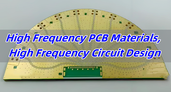
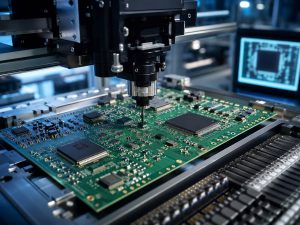
High-speed PCB is used in electronic products where fast signal transmission, impedance stability, and low noise are essential to system performance. Once signal frequency rises, data rate increases, or edge transitions become faster, standard PCB layout rules are no longer enough. At that stage, the board must be engineered for signal integrity, EMI control, stack-up stability, and manufacturability.
EBest Circuit (Best Technology) provides high-speed PCB manufacturing for applications that require reliable transmission performance, including telecommunications, automotive electronics, aerospace systems, networking hardware, industrial control, medical electronics, and RF-related products. We support customers from prototype through volume production with practical engineering review, controlled process capability, and material options suited for high-speed designs.
Why Does High-Speed PCB Design Matter in Modern Electronics?
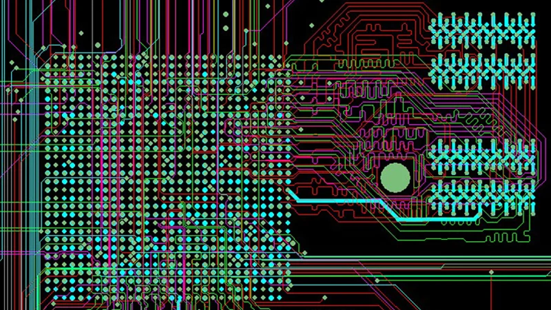
High-speed PCB design matters because fast signals do not behave like ordinary low-speed connections. As frequency increases and edge rates become sharper, the PCB trace begins to act like a transmission line. That means routing length, impedance variation, dielectric material, grounding, and via structure can all change the final electrical result.
If these factors are not handled correctly, the system may face signal reflection, crosstalk, EMI issues, timing mismatch, data errors, and unstable communication between devices. This is why high-speed PCB is not simply a faster version of a standard board. It is a different design discipline that requires electrical and manufacturing control from the beginning.
What Is a High-Speed PCB?
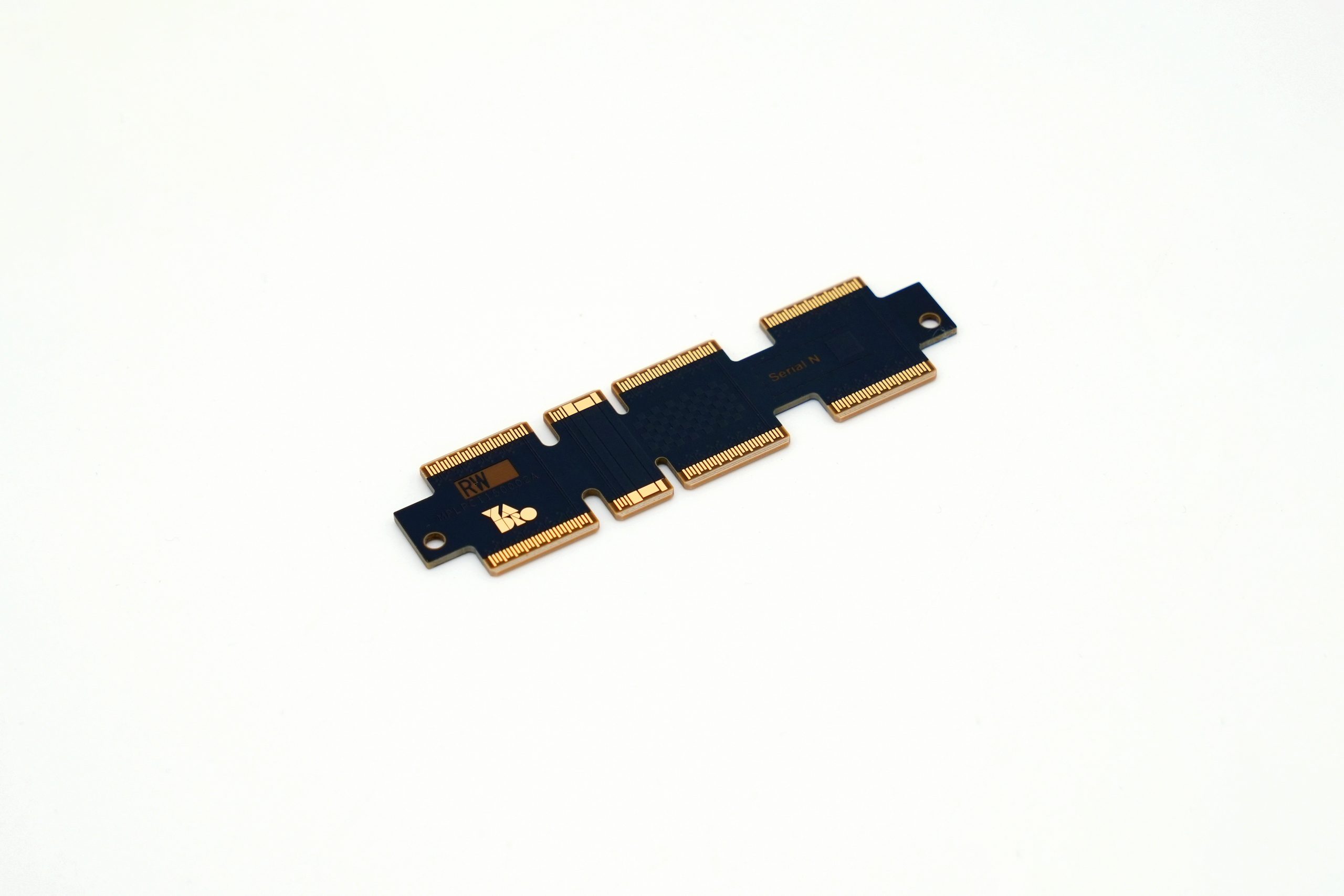
A high-speed PCB is a printed circuit board developed for circuits where signal integrity becomes a major design requirement. In many practical cases, high-speed conditions are associated with one or more of the following: operating frequency above 50 MHz, transmission rate above 1 Gbps, or rise and fall time below 500 ps.
In practical engineering terms, a board should be treated as high-speed when signal quality can be affected by impedance mismatch, trace discontinuity, return path interruption, material loss, delay mismatch, or noise coupling. Once any of these begin to affect performance, the PCB must be designed as a high-speed platform rather than a conventional one.
High-Speed PCB vs. Low-Speed PCB: What Is the Difference?
The real difference between a high-speed PCB and a low-speed PCB is not only clock frequency. The larger difference is how tightly the board must control electrical behavior to preserve signal quality and stable transmission.
| Item | Low-Speed PCB | High-Speed PCB |
|---|---|---|
| Signal behavior | Less sensitive | Highly sensitive |
| Impedance control | Often not critical | Essential |
| Trace routing | Basic design rules | Strict electrical design rules |
| EMI concern | Lower | Much higher |
| Material demand | Standard FR4 often enough | May require low-loss laminate |
| Timing control | Less critical | Important for reliability |
| Stack-up planning | Functional | Performance-driven |
This comparison matters because many design issues appear when a board is still being treated like a conventional PCB even though the signals already behave like high-speed channels.
Are You Facing These High-Speed PCB Challenges?
Many OEMs, design houses, and sourcing teams run into the same issues when developing high-speed boards. The layout may look complete, but performance problems often appear during bring-up, test, or volume production.
- Differential pair mismatch
- Reflection caused by poor impedance control
- Crosstalk between adjacent signal lines
- EMI failure in dense multilayer boards
- Excessive insertion loss at high frequency
- Unstable routing performance between prototype and mass production
- Material selection that does not match the actual signal requirement
- Layout structures that are hard to manufacture consistently
These challenges are especially common in designs using PCIe, USB, Ethernet, HDMI, SATA, LVDS, and MIPI. When signal integrity, EMI, thermal behavior, power distribution, and component placement are not handled well, product performance can suffer quickly.
How Do We Help Solve High-Speed PCB Problems?
At EBest Circuit, we do more than fabricate copper patterns. We help align design intent with manufacturing reality so the finished board performs more predictably in actual use.
- Material suggestion based on speed and loss targets
- Stack-up review for impedance and return path stability
- Controlled impedance manufacturing support
- Routing manufacturability feedback
- Process planning for multilayer and via structures
- Prototype support for early validation
- Stable transition from sample to production
This approach helps customers reduce design rework, shorten validation cycles, and improve consistency across builds.
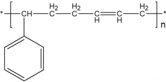
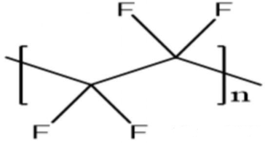
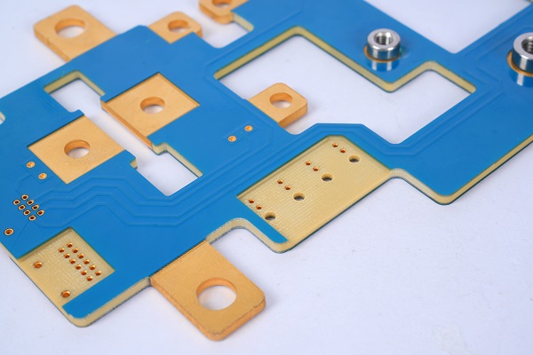
What Materials Are Best for High-Speed PCB?
Dielectric material selection is essential because it affects how quickly and how cleanly signals travel through the PCB. In high-speed applications, lower dielectric constant materials are often preferred because they support faster signal propagation and lower loss.
| Material | Typical Dk | Performance Characteristics | Typical Applications |
|---|---|---|---|
| Standard FR4 | ~4.5 | Cost-effective, suitable for moderate-speed designs | General electronics, some digital boards |
| Low-Loss FR4 | Lower than standard FR4 | Better signal performance, improved loss behavior | Embedded systems, communication products |
| Rogers 4000 / 3000 Series | ~2.0–3.5 | Low loss, stable electrical performance | RF, telecom, automotive radar |
| PTFE | ~2.0–2.5 | Very low loss for very high-frequency applications | 5G, microwave, aerospace, radar |
Material selection should not be based on cost alone. It should be based on the actual signal environment, channel loss budget, interface type, and board structure.
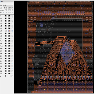
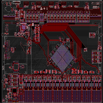
What Are the Most Important High-Speed PCB Design Rules?
High-speed PCB design works best when electrical rules are defined early and followed consistently throughout the layout. A strong design must balance signal performance with practical manufacturability.
1. Control Impedance Carefully
Critical traces must maintain consistent impedance from source to load. Any sudden change can create reflections and degrade signal quality.
2. Build the Right Stack-Up
A good stack-up places signal layers next to solid reference planes. This improves return path continuity and reduces EMI.
3. Keep Trace Length Practical
Longer routes increase delay and loss. Critical nets should stay as short and direct as possible.
4. Reduce Crosstalk
Parallel routing should be limited, and spacing should be sufficient to reduce coupling between signal lines.
5. Route Differential Pairs Correctly
Differential pairs need consistent spacing, matched length, and stable reference conditions.
6. Manage Via Effects
Vias add parasitic inductance and capacitance. Poor via usage can hurt signal quality, especially in dense high-speed layouts.
7. Improve Power Integrity
Stable power delivery is important because high-speed ICs are sensitive to supply noise.
8. Optimize Component Placement
Key components should be placed to reduce routing complexity and improve signal path quality.
Which Interfaces Require High-Speed PCB Design?
Many modern electronic products rely on interface standards that demand strong high-speed layout and manufacturing control.
- PCIe for high-speed peripheral data transfer
- USB for fast communication and storage
- Ethernet for networking up to high data rates
- HDMI for high-bandwidth video and audio
- SATA for storage communication
- LVDS for displays and cameras
- MIPI for mobile and embedded camera or display systems
When these interfaces are present, stack-up design, impedance control, pair routing, and connector transition quality become much more important.
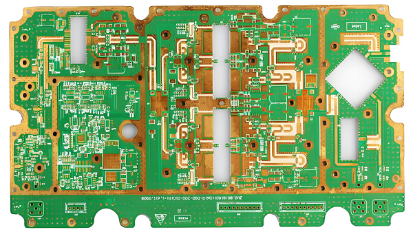
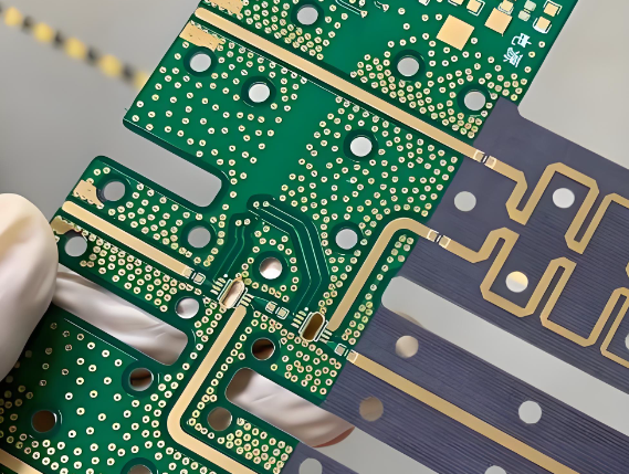
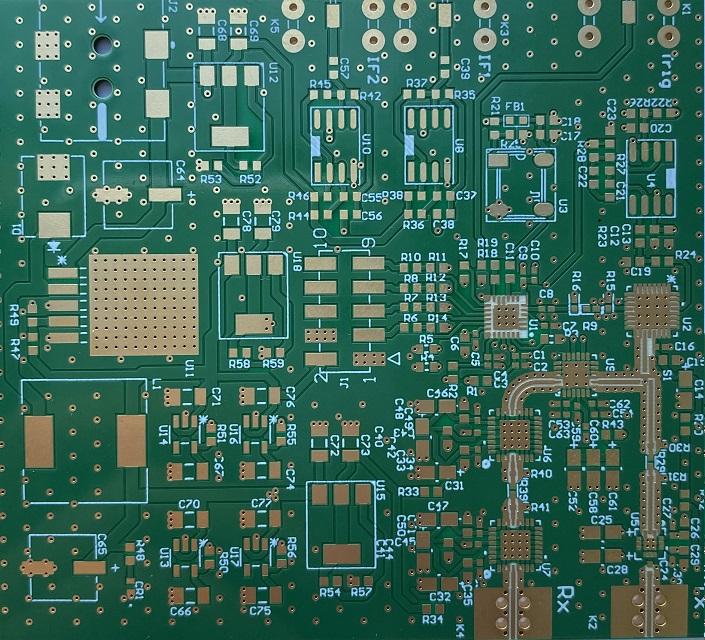
How Is a High-Speed PCB Manufactured?
The manufacturing flow of high-speed PCB is more demanding than standard PCB because even small process variation can influence electrical performance. A reliable process must support both structural accuracy and repeatable signal behavior.
1. Material Selection
The correct laminate is chosen based on dielectric constant, signal frequency, and loss requirement.
2. Layer Stack-Up Design
Signal, power, and ground layers are arranged to support impedance targets and EMI control.
3. Trace Width Calculation and Impedance Control
Trace width and spacing are verified to match single-ended or differential impedance requirements.
4. Lamination
Multilayer panels are bonded under controlled pressure and temperature.
5. Drilling and Via Formation
Through holes, blind vias, buried vias, or microvias are created based on design need.
6. Copper Plating
Plating forms conductive connections between layers and helps ensure electrical reliability.
7. Etching
Precision etching defines trace width and spacing, which directly affects impedance.
8. Solder Mask and Silkscreen
Protective coating and identification marking are added.
9. Surface Finish
Common finish options include ENIG, OSP, and immersion silver.
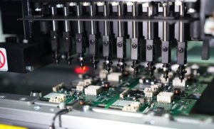
10. Testing and Inspection
Final checks confirm electrical continuity, dimensional control, and manufacturing quality.
Why Choose EBest Circuit as Your High-Speed PCB Manufacturer?
For high-speed PCB projects, manufacturing experience matters because electrical performance depends on how well the design is translated into the real board. A supplier that understands only fabrication may miss what actually matters to the final product.
- Support for impedance-controlled high-speed PCB fabrication
- Experience with FR4, low-loss materials, Rogers, and PTFE-based builds
- Engineering review for stack-up and manufacturability
- Prototype and production support
- Stable multilayer process control
- One-stop PCB and PCBA support when required
- Application experience across telecom, automotive, aerospace, industrial, and RF-related products
We focus on helping customers improve both performance and production stability, not only getting the board built.
What Applications Use High-Speed PCB?
High-speed PCBs are used in many industries where fast signal transmission and reliable electrical performance are essential.
- Telecommunications equipment
- Automotive electronics and radar systems
- Aerospace electronics
- 5G infrastructure
- Data centers
- Defense systems
- Medical devices
- Networking equipment
- RF and microwave systems
- Industrial electronic control products
As data rates continue to rise across industries, high-speed PCB design is becoming a standard requirement in more product categories.
What Should You Look for in a High-Speed PCB Supplier?
If you are selecting a manufacturer, it helps to evaluate more than price and lead time. A better supplier should also understand the electrical side of the board.
- Knowledge of signal integrity basics
- Material options for different speed ranges
- Controlled impedance capability
- Multilayer stack-up support
- Stable drilling, plating, and etching control
- Clear communication during DFM review
- Reliable prototype-to-production consistency
This reduces the chance of performance drift between sample builds and mass production orders.
Need a High-Speed PCB Quote for Your Project?
If your design includes fast data channels, impedance-sensitive routing, or multilayer architecture with demanding electrical requirements, we can help. EBest Circuit (Best Technology) provides high-speed PCB support from engineering review through fabrication and delivery.
Send us your Gerber files, stack-up, impedance requirements, or project specifications, and we will review the best manufacturing solution for your application.
FAQ About High-Speed PCB
1. What is considered a high-speed PCB?
A PCB is commonly treated as high-speed when the operating frequency is above 50 MHz, the data rate exceeds 1 Gbps, or the signal rise and fall time is below 500 ps.
2. Can FR4 be used for high-speed PCB?
Yes. FR4 can be used in some moderate-speed applications. For higher-frequency or lower-loss designs, Rogers or PTFE-based materials may be more suitable.
3. Why is impedance control important in high-speed PCB?
Impedance control helps reduce signal reflection and preserves waveform integrity during fast transmission.
4. What interfaces usually need high-speed PCB design?
PCIe, USB, Ethernet, HDMI, SATA, LVDS, and MIPI are common examples.
5. What surface finishes are used for high-speed PCB?
Common options include ENIG, OSP, and immersion silver.
6. Which industries use high-speed PCBs?
Telecommunications, automotive, aerospace, 5G, medical, defense, networking, and RF-related industries all use high-speed PCBs.