When you look inside an LED lighting product, you’ll often find a small but essential component called the LED driver board. This little board plays a big role in making sure your lights work properly and last longer. But what exactly is a LED driver board? How does it work? And how can you tell if one is faulty?
In this blog, we’ll walk through everything you need to know—from how it functions to how to test it and where it’s used.
What Is a LED Driver Board?
A LED driver board is an electronic circuit that regulates power to LEDs. LEDs don’t work directly from AC power like traditional light bulbs. They need a constant DC current at a specific voltage to operate correctly. Without proper regulation, LEDs may overheat, flicker, or fail prematurely.
The LED driver board manages this power conversion and ensures stable operation. It’s like a power supervisor, controlling the flow of energy to keep everything within safe limits.
Types of LED Driver Boards
There are several types of LED light driver boards, each serving a different need depending on the application:
1. Constant Current LED Driver Boards
These provide a fixed current to the LEDs while allowing the voltage to vary. They are used in high-power LEDs where current regulation is critical. These boards prevent overdriving the LED, which can cause heat buildup and burnout.
2. Constant Voltage LED Driver Boards
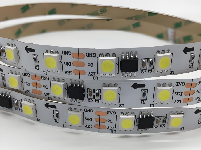
These deliver a fixed voltage output (usually 5V, 12V, or 24V) while the current changes depending on the load. These are commonly used in LED strips or low-power lighting where LEDs are connected in parallel.
3. AC-DC Driver Boards
These convert 120V or 220V AC power from wall outlets into low-voltage DC suitable for LEDs. They include rectifiers and smoothing circuits to provide clean power.
4. Dimmable LED Driver Boards
Some driver boards allow users to adjust brightness. These can use dimming methods like:
- TRIAC dimming (phase-cut dimming for residential AC power)
- PWM dimming (pulse-width modulation for digital control)
- 0-10V dimming (analog dimming for commercial lighting)
5. Smart LED Driver Boards
Modern lighting products use intelligent driver boards with features like:
- Over-voltage and over-current protection
- Temperature monitoring
- Wireless control via Bluetooth or Wi-Fi
- Programmable lighting behavior
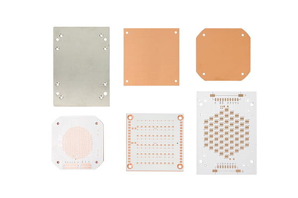
Raw Materials in LED Driver Boards
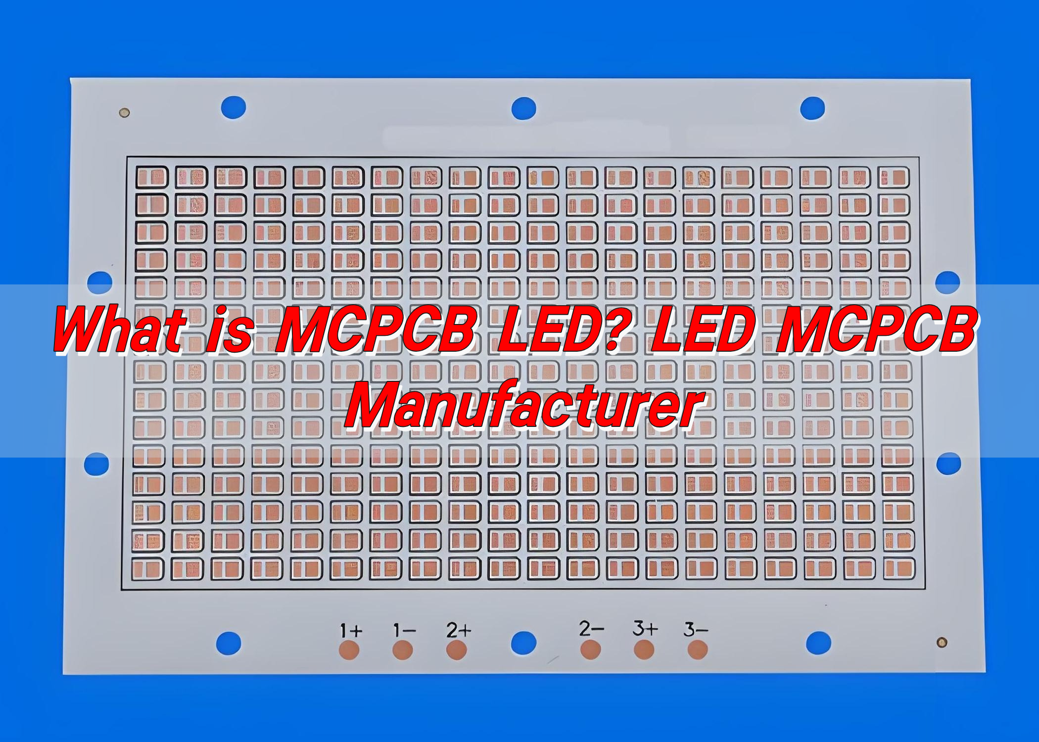
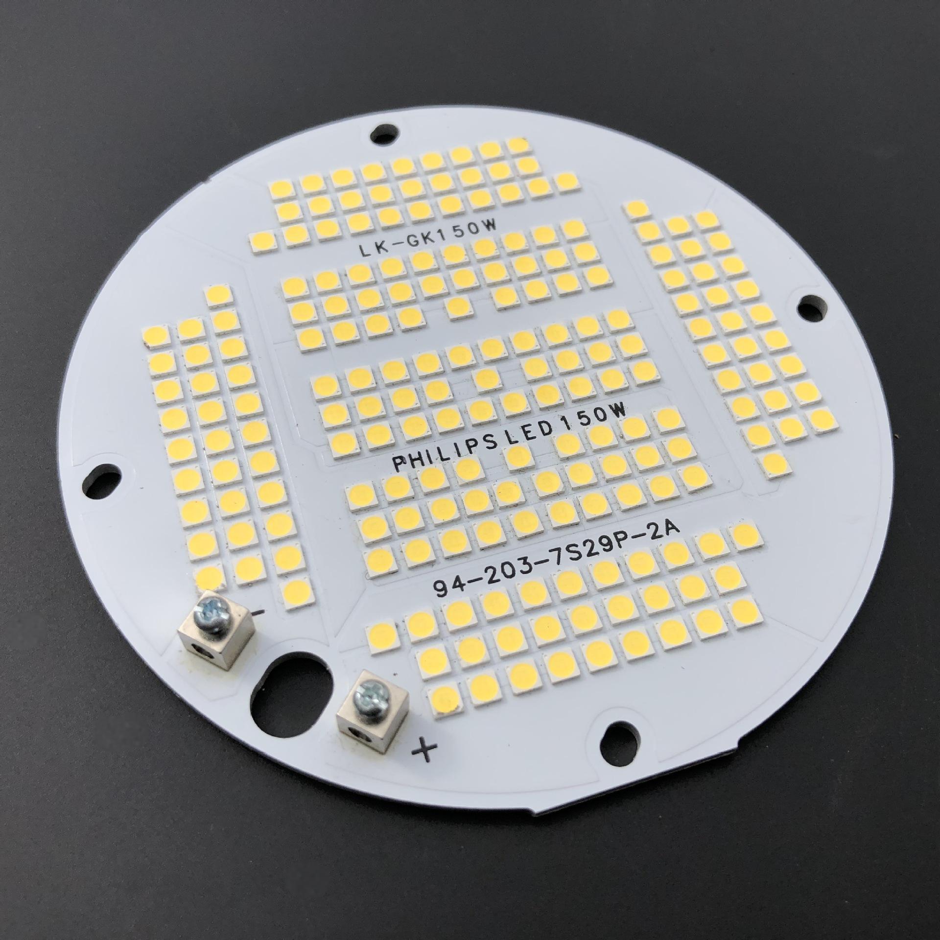
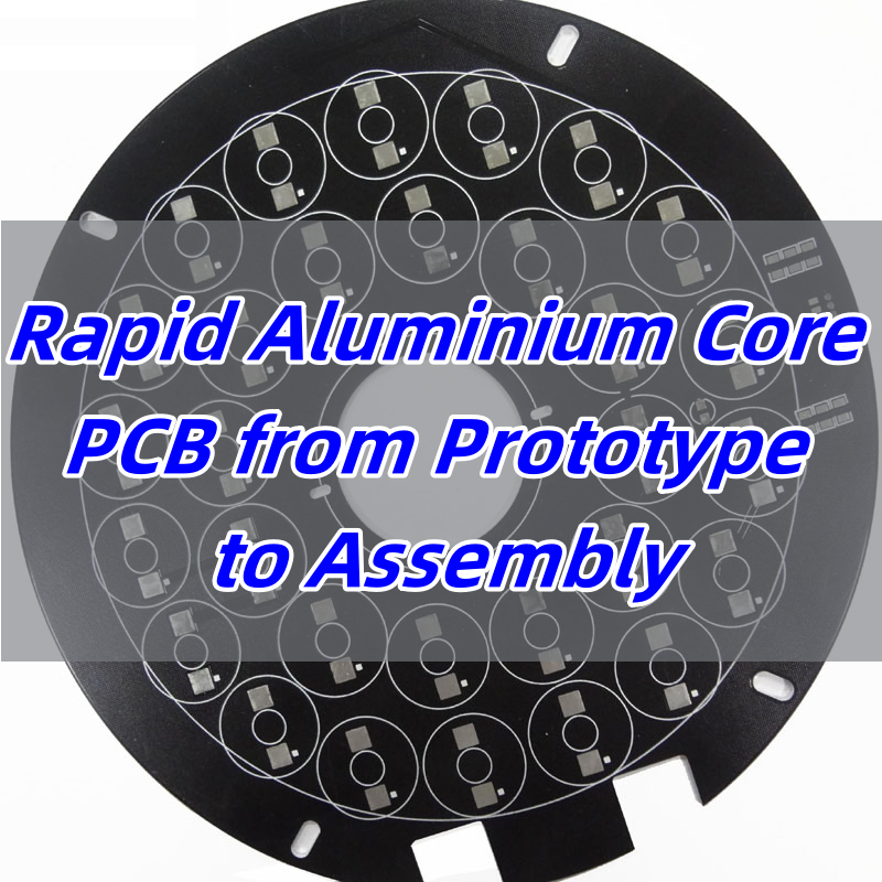
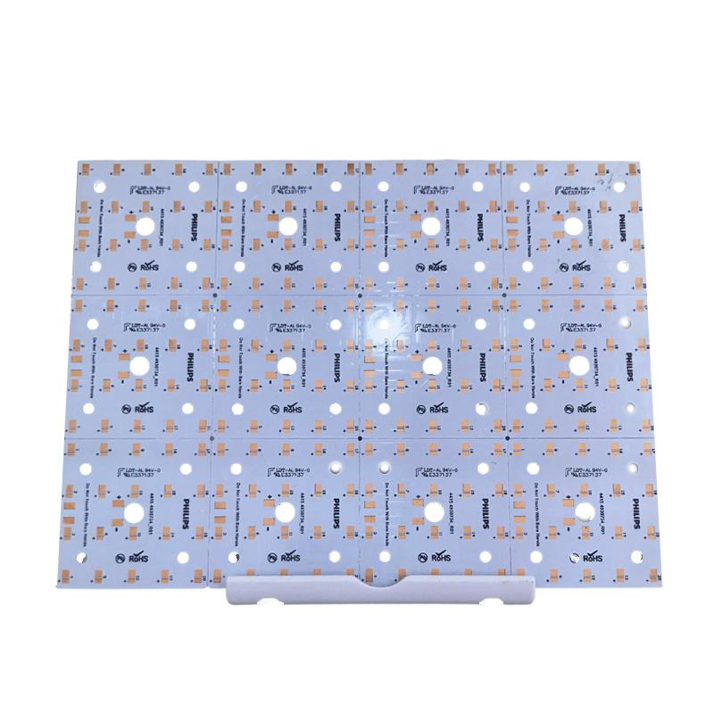
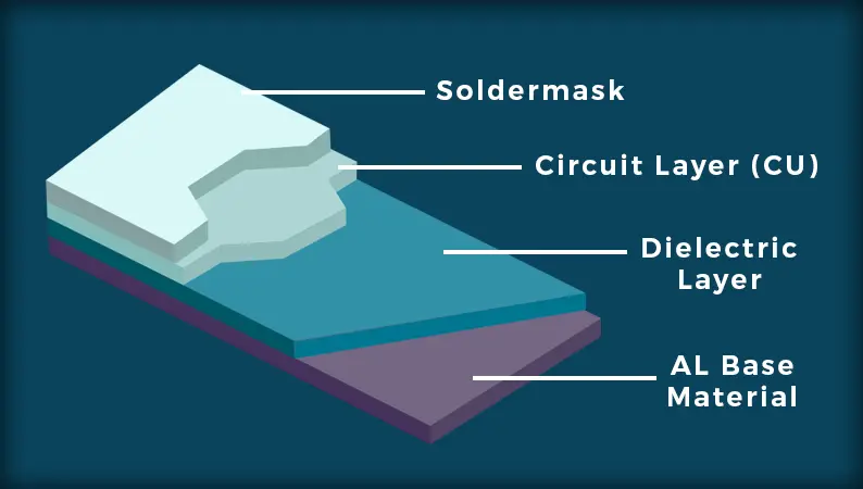
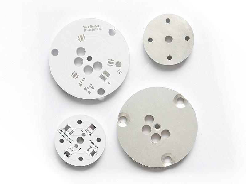
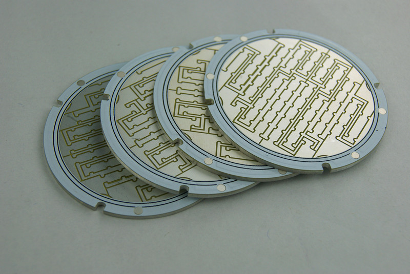
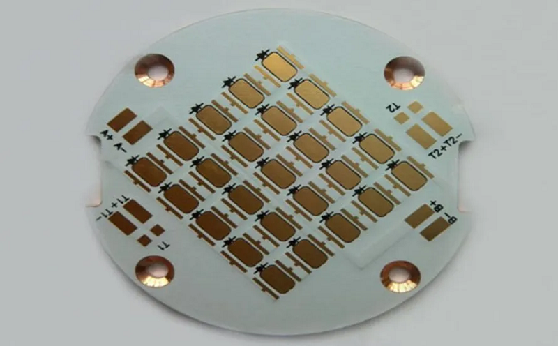
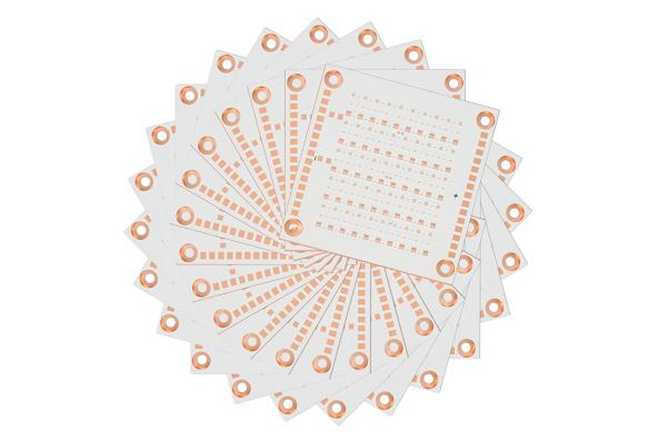
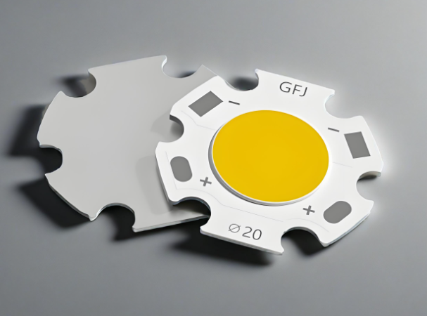
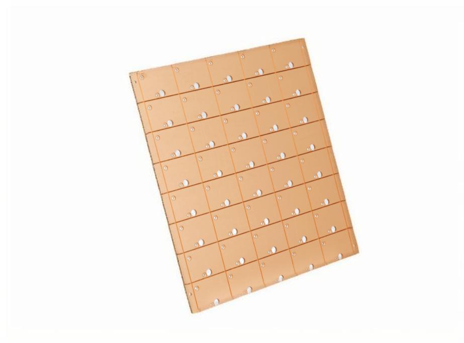
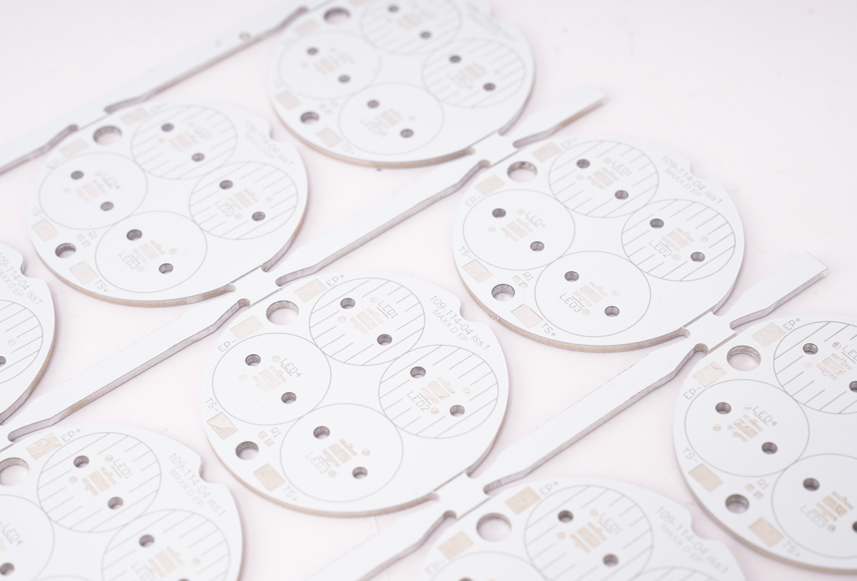
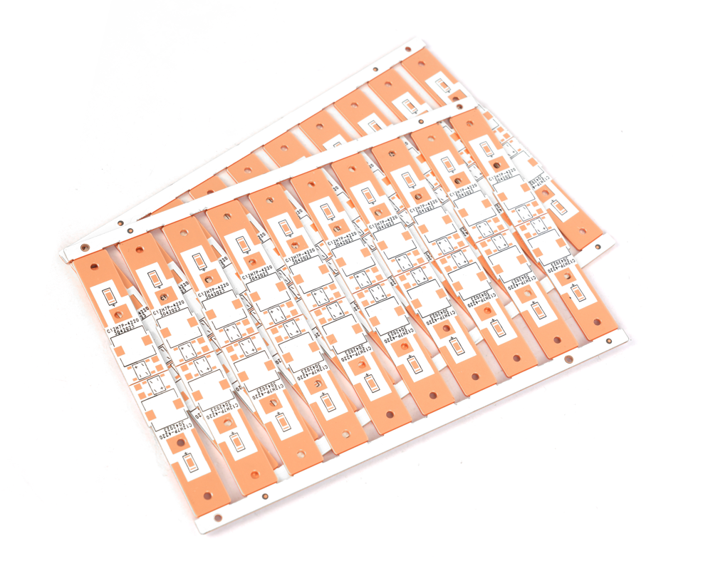
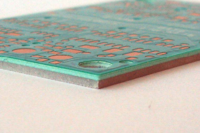
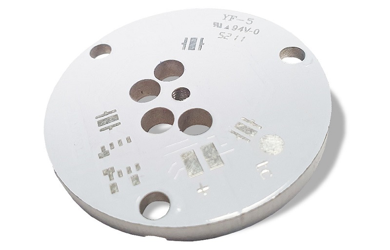
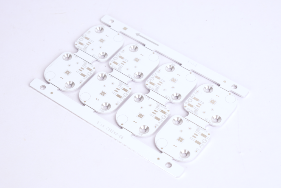
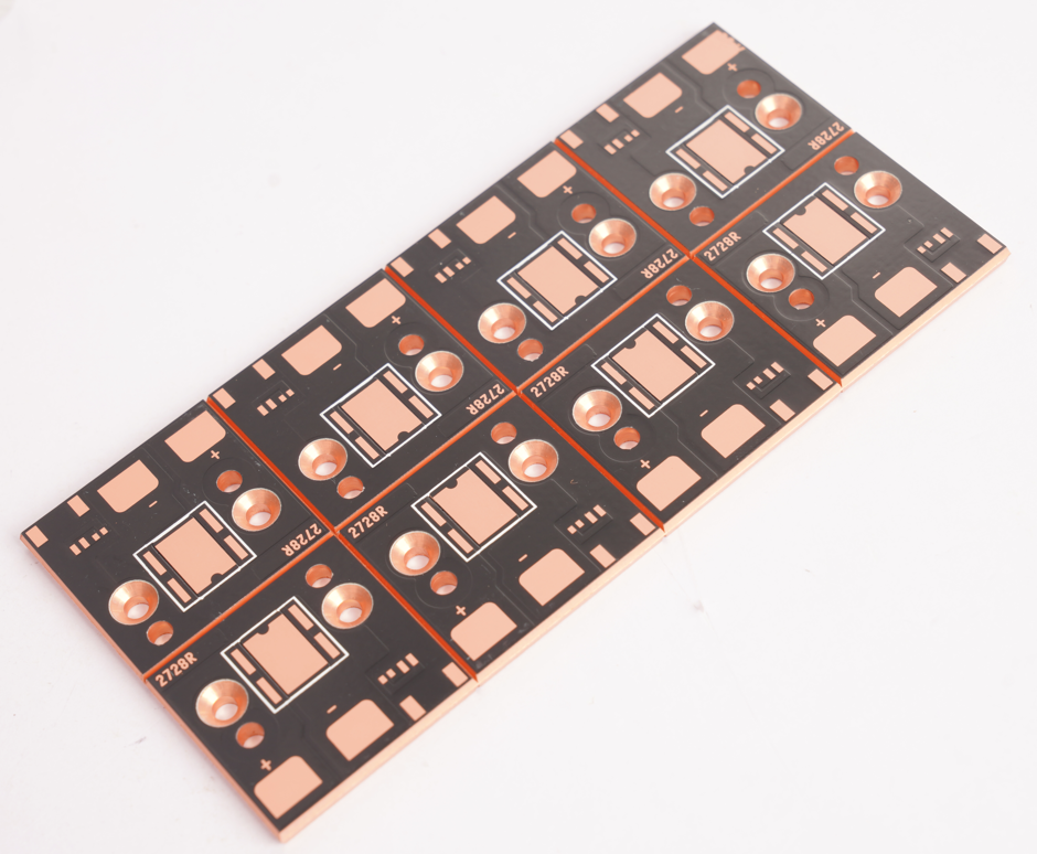
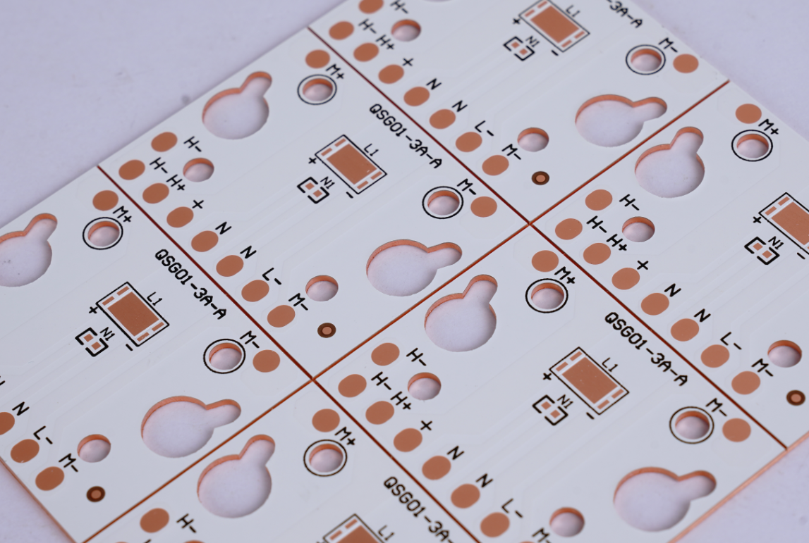
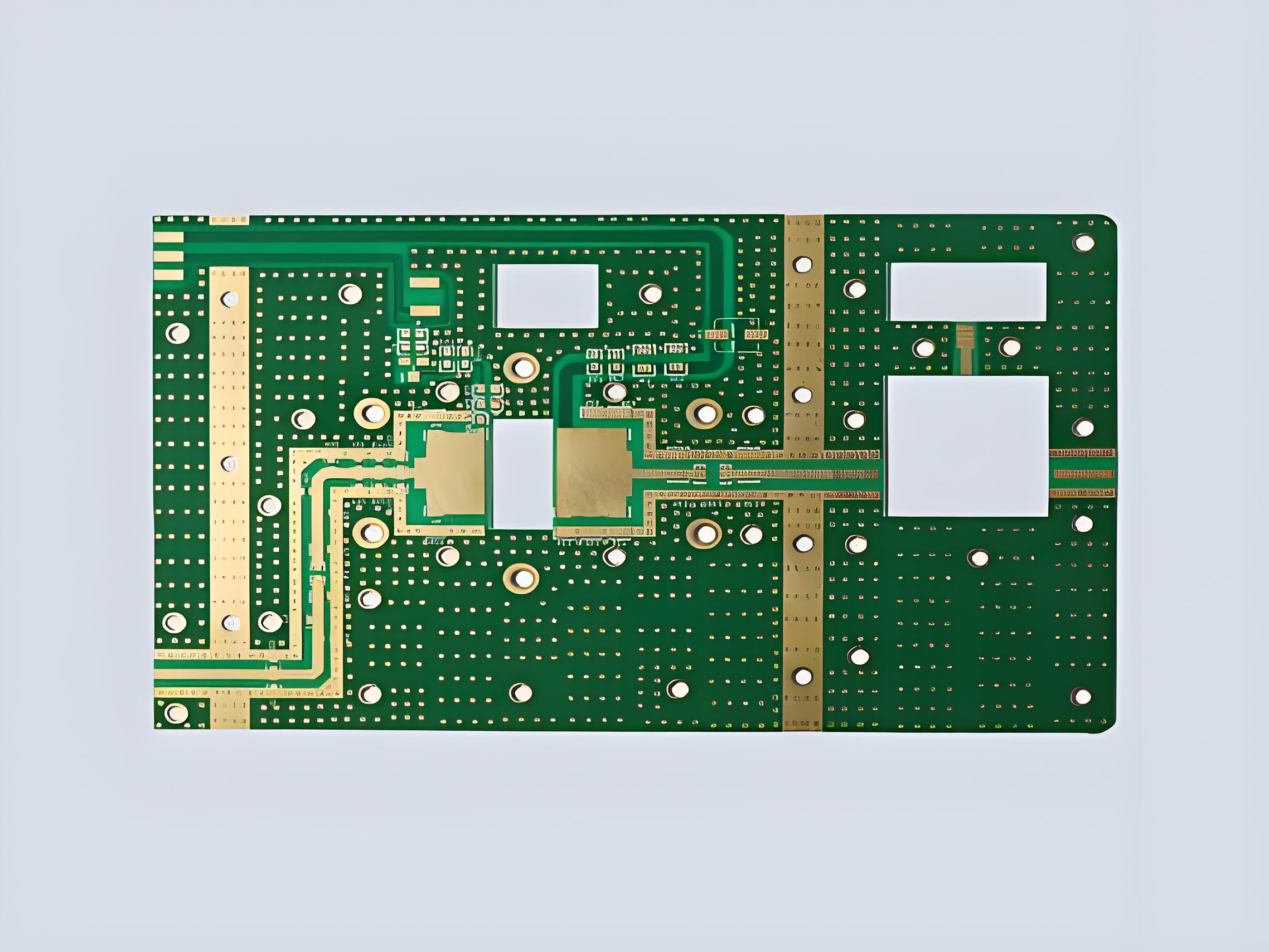
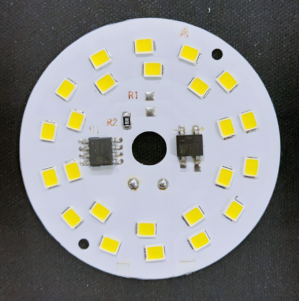
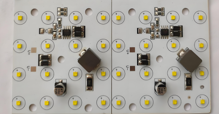
one of the most important materials of LED driver board is the aluminum LED PCB. Unlike standard FR4 boards, aluminum PCBs use aluminum base as its core, which offers excellent heat dissipation and it is critical for the longevity and performance of LED lighting systems.
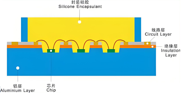
Aluminum LED board consists of an aluminum base (like 5052, 6061 aluminum alloy), a thermally conductive dielectric layer, and a copper circuit layer. The aluminum base transfers heat away from the LED components, allowing for higher power densities and improved reliability, especially in high-brightness or high-wattage applications like automotive headlights, floodlights, and industrial lamps.
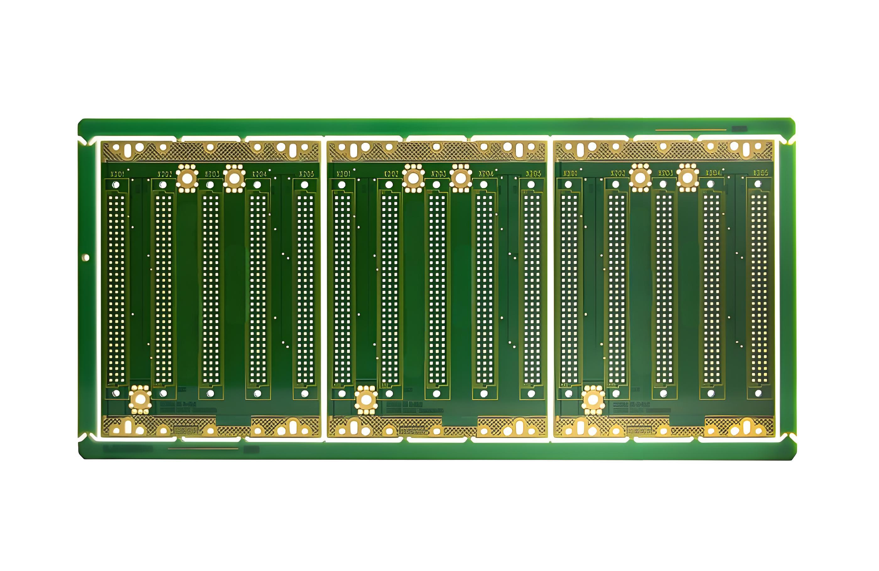
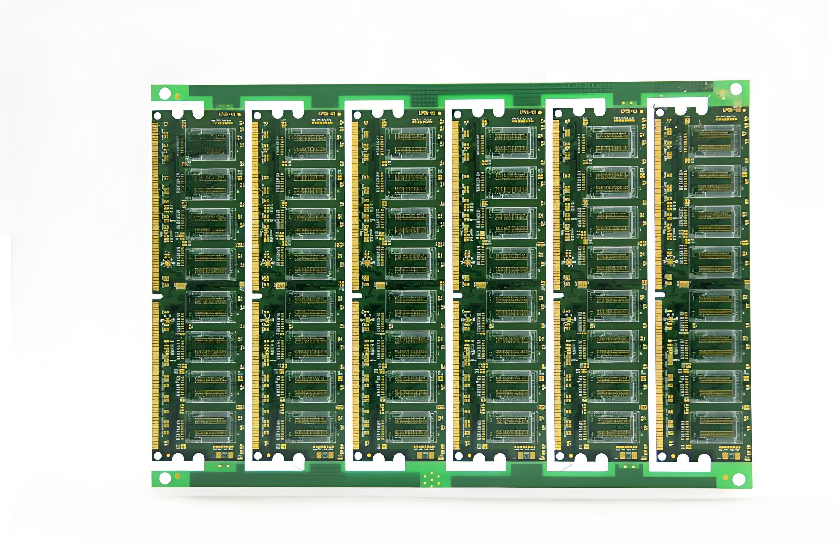
In addition to the aluminum substrate, LED driver boards use a variety of other materials like copper, electronic components, control ICs, and so on. When all these materials are integrated on an aluminum PCB, the result is a durable, thermally stable driver board that supports long-lasting LED performance even under demanding conditions.
How Does a LED Light Driver Board Work?
A LED light driver board works by converting high-voltage AC power from the mains into low-voltage DC power suitable for driving LEDs. This process typically involves several stages, starting with a rectifier circuit that changes AC to DC, followed by filtering capacitors that smooth the voltage. After that, a switching regulator or linear regulator adjusts the voltage and current to match the LED’s requirements. For constant current drivers, the circuit controls the output current precisely to protect the LED from overcurrent damage. Below is a simple led driver board schematic drawing for reference:
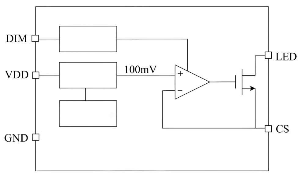
Inside the board, components like MOSFETs, control ICs, and feedback loops work together to maintain stable power output, even if the input voltage or load conditions change. Advanced LED driver boards also include safety features like overvoltage, short-circuit, and thermal protection. Some models support dimming and intelligent control through PWM signals or 0–10V inputs.
What Does a LED Driver Board Do?
In simple terms, the LED driver board ensures your LEDs operate the way they’re supposed to. Here’s what it really does:
- Regulates current and voltage so LEDs don’t get too much or too little power
- Extends lifespan by preventing overheating and electrical stress
- Protects the circuit from power surges, short circuits, and reverse polarity
- Improves performance by maintaining consistent light output even when the power supply varies
Without a proper driver board, even the best LED won’t last long.
What Are the Symptoms of a Bad LED Driver Board?
A malfunctioning LED driver board can cause several problems. If your LED light is acting up, here are some signs the driver board might be the culprit:
- Flickering light even when power is steady
- Dim or unstable brightness
- Completely dead light while the power source works
- Unusual buzzing sounds from the driver
- Overheating of the driver board or the LED
- Shortened lifespan of the LED itself
If you notice any of these issues, it’s worth checking the driver before replacing the whole lighting system.
How to Test LED Driver Board with Multimeter?
Before testing, make sure you have a digital or analog multimeter with a fully charged battery. Depending on what you’re testing, you will need to switch between the DC voltage, DC current, and resistance (ohm) settings. Here are the ways to test a led driver board step by step in simple ways:
1. Tools Preparation:
- Use a digital or analog multimeter.
- Make sure the power is off before testing, unless checking voltage under load.
- Know the driver’s rated voltage and current (e.g., 12V, 300mA).
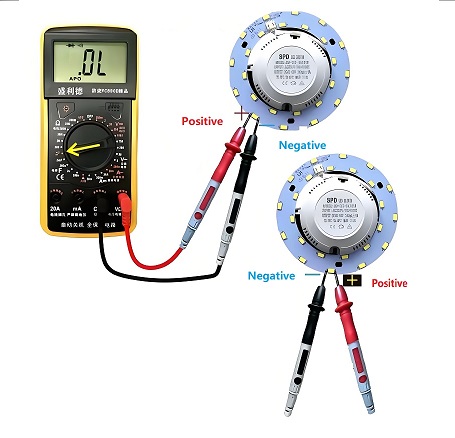
2. Test Output Voltage (DC):
- Set the multimeter to DC voltage mode (e.g., 20V or 50V).
- Connect the red probe to the driver’s positive output and black to the negative.
- Power on the driver. A normal 12V driver should read between 11.5V and 12.5V.
- Zero or very low voltage may indicate failure.
3. Test Output Current:
- Disconnect the LED from the driver.
- Set the multimeter to DC current mode (e.g., 200mA).
- Connect the multimeter probes in series with the circuit.
- A good driver should output current close to the rated value (e.g., 280–320mA for a 300mA driver).
4. Test Output Resistance (When Powered Off):
- Set the multimeter to resistance mode (200Ω or 2kΩ).
- Measure resistance across the output terminals.
- Normal resistance is typically between 50–500Ω.
- 0Ω suggests a short circuit, while infinite resistance suggests an open circuit.
Common Problems Found During Testing
| Symptom | Likely Cause |
| No output voltage | Burnt rectifier, blown fuse, or shorted components |
| Low voltage | Faulty regulator IC or degraded capacitor |
| High ripple | Dried-out electrolytic capacitor |
| No input power | AC not reaching board or blown input fuse |
| Flickering LEDs | Intermittent driver output or voltage instability |
| No continuity | Open trace or failed resistor/fuse |
Testing a LED driver with a multimeter is a straightforward but powerful way to troubleshoot lighting systems. If the driver fails any of the above tests, especially with incorrect voltage or current output, it should be replaced to prevent damaging the LED module.
At EBest Circuit (Best Technology), we offer custom LED driver boards, professional testing, and aluminum PCB solutions for LED lighting systems. Whether you’re designing new products or diagnosing a problem in the field, our team is here to support you with precision manufacturing and technical advice.
LED Light Driver Board Applications
- Indoor Lighting: Bulbs, downlights, panel lights, smart lighting
- Outdoor Lighting: Streetlights, tunnel lights, floodlights
- Automotive Lighting: Headlights, taillights, DRLs, interior lighting
- Signage & Displays: LED billboards, backlit signage, LCD TV backlighting
- Industrial Systems: High-bay warehouse lights, machine vision lighting
- Medical Devices: Examination lights, operating room lights
- Smart Homes: Voice or app-controlled LED lamps
LED Driver Board HS Code
When importing or exporting LED drivers, it is crucial to classify them under the correct Harmonized System (HS) codes to comply with customs regulations and avoid delays or penalties. The HS code varies depending on the specific type of LED product or component involved. Below are common HS codes relevant to LED drivers and related products.
| Product Type | Typical HS Code | Description |
| LED Bulbs/Tubes | 8539.50.00 | LED replacement light sources (finished bulbs) |
| LED Driver Power Supplies | 8504.40.14 | LED driver modules, transformers, power supplies |
| LED Display Modules | 8531.20.00 | LED-based digital display units |
| Complete LED Fixtures | 9405.42.90 / 9405.50.00 | Finished lighting fixtures and lamps |
Note: Always check your country’s customs database or consult a logistics expert for precise classification, as some driver boards integrated into complete lighting units may have different codes.
FAQs
1. Can I repair a damaged LED driver board?
Yes, if the issue is minor (like a bad capacitor), it can be repaired. But for safety-critical lighting, replacement is often better.
2. What’s the difference between an LED driver and a power supply?
An LED driver includes current regulation and protection circuits, whereas a basic power supply may only convert voltage.
3. Is aluminum PCB necessary for LED driver boards?
For high-power lighting, yes. Aluminum PCBs help dissipate heat better than FR-4 boards.
4. How long does a LED driver board last?
Most LED drivers last between 30,000 and 50,000 hours, depending on load and cooling.
5. Can a single driver power multiple LEDs?
Yes, if wired correctly and within the driver’s power capacity. Parallel connections need constant voltage drivers; series connections use constant current drivers.
This is the end of this sharing, if you are interested in LED driver board that used in aluminum base or copper base or FR4 base, you are welcome to contact us. EBest Circuit (Best Technology) is a 19 years experienced PCB & PCB assembly manufacturer in China, we have SMT factory both in China Shenzhen and Vietnam. We are welcome your visiting or any comments.