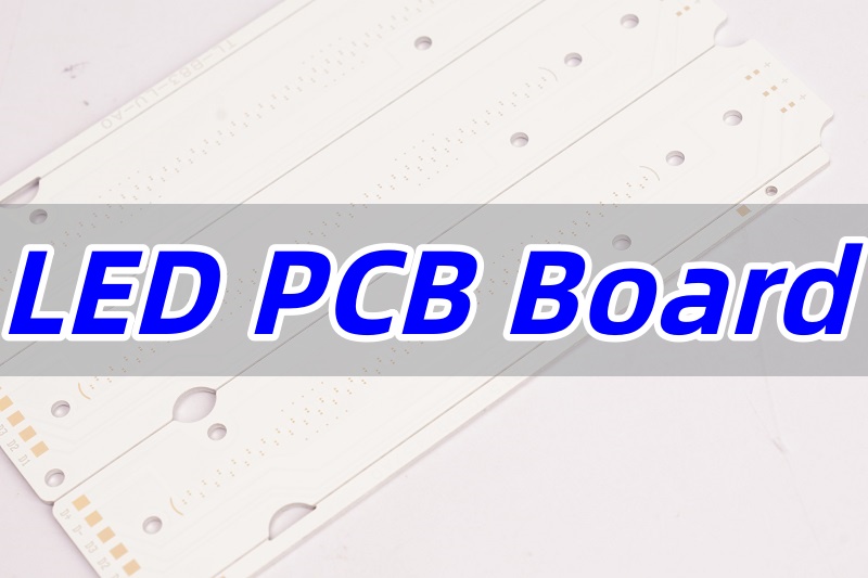
LED PCB board is the backbone of modern lighting. The blog shares valuable points on the design, construction, testing, and diverse applications of LED PCB boards, including differences between power ratings, features of LED strip PCBs, and guidance for sourcing high-quality prototypes.
Are there major challenges hindering your LED PCB board project?
- Improper thermal design causes overheating and shortens lifespan?
- Inconsistent manufacturing quality, such as uneven brightness, flickering, or varying lifespans?
- Design difficulties and long production cycles?
- High-quality LED PCB boards are costly, and your customers choose cheaper products, potentially sacrificing quality?
Here’s how we tackle the issues mentioned above:
- Optimized Thermal Management: Using metal-core PCBs (MCPCB) and advanced thermal design to improve heat dissipation efficiency.
- Enhanced Quality and Consistency: Employing advanced manufacturing equipment and strict quality control processes to ensure product uniformity.
- Technical Support and Project Management: Providing technical support and project management services to guide clients through the entire process from design to delivery.
- Cost and Performance Balance: Offering high cost-performance solutions that balance budget constraints with product performance.
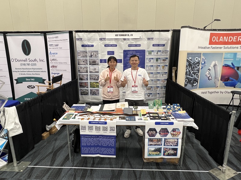
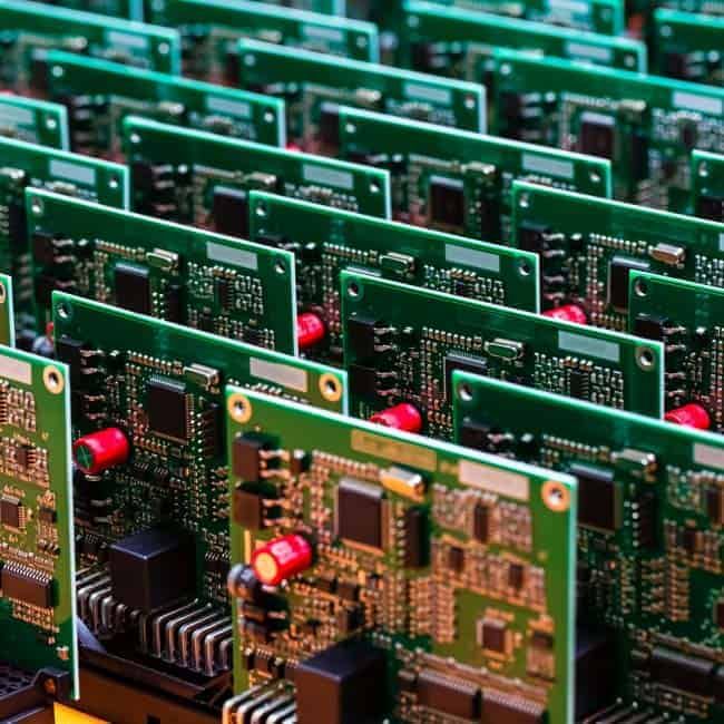
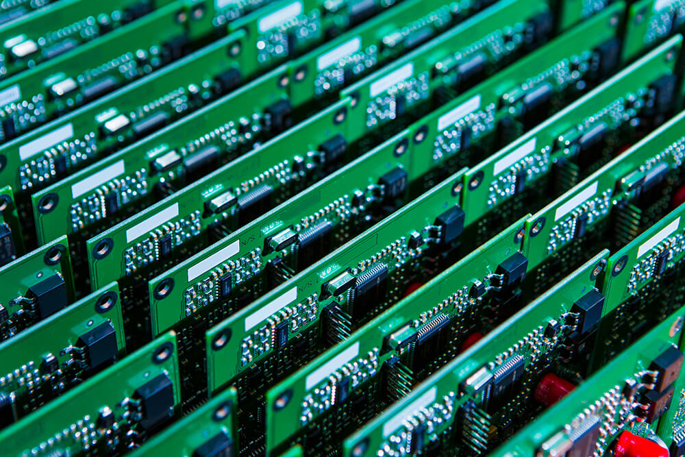
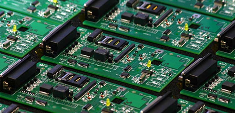
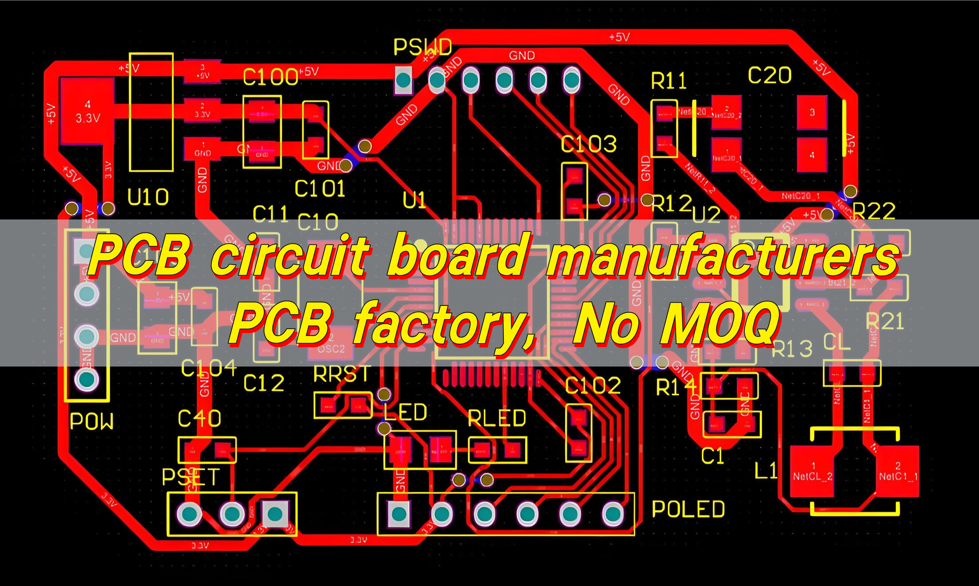
As a PCB light board manufacturer, EBest Circuit (Best Technology) provides custom LED PCB, SMD LED PCB board prototypes, LED PCB board design, mass production, LED PCB board 12v assembly, LED PCB Strip box build service. We have our own metal core PCB factory, responsible for expediting your delivery time, quality control, and full process coordination. You don’t need to waste time and money to communicate with different factories. Since you cooperate with EBest Circuit (Best Technology), which is a one-stop PCB and PCBA factory. If you have any doubts or requirements about LED PCB board material selection, LED PCB board prototypes, or LED PCB fabrication, just feel free to make contact with us through sales@bestpcbs.com.
What is LED PCB Board?
An LED PCB board (Light Emitting Diode Printed Circuit Board) is a specialized circuit board designed to mount, connect, and power LED components. It not only provides electrical pathways but also supports the LEDs mechanically and manages heat efficiently, ensuring stable illumination and extended lifespan. In essence, LED PCB boards form the backbone of modern lighting systems, supporting everything from small LED PCB boards to large-scale LED display PCB boards.
Key Components and Structure
- Substrate: The base material, which can vary from standard FR4, aluminum, or ceramic, is chosen based on thermal management requirements. For instance, aluminium PCB boards for LED are widely used in high-power applications due to their excellent heat dissipation.
- Copper Layer: Conductive traces transmit power from the input terminals to each LED. The thickness and layout of the copper layer determine current carrying capacity and light output stability.
- Solder Mask: This protective layer prevents short circuits and oxidation while providing a reliable surface for soldering LEDs and other components.
- Pads: Areas where LEDs and resistors are mounted, ensuring both electrical connectivity and mechanical stability.
- Surface Finish: Treatments like ENIG or HASL enhance solderability and protect copper traces.
Why It’s Important / Core Advantages
- Efficient Thermal Management: With metal-core designs like MCPCB or aluminium LED PCB boards, heat generated by high-power LEDs is dissipated effectively, preventing overheating.
- Enhanced Brightness and Efficiency: Optimized circuitry reduces energy loss, improving luminous efficiency for LED strip PCB boards, RGB LED PCB boards, and other configurations.
- Extended Lifespan: Proper heat control and reliable construction reduce the risk of premature failure, especially in LED ceiling light PCB boards or LED tube light PCB boards.
- Flexible Design Options: Whether for custom LED PCB boards or high-density SMD LED PCB boards, layouts can be tailored to fit specific applications.
Difference from FR4
- While FR4 is a common material for standard circuit boards, offering low cost and good insulation, its thermal conductivity is limited.
- In contrast, LED PCB boards often use metal or ceramic substrates to handle higher power and manage heat efficiently, crucial for maintaining consistent brightness and long-term reliability. The choice of board material—be it aluminium LED PCB board, LED PCB board material for high-wattage setups, or FR4 for low-power designs—directly affects thermal performance, current handling, and overall efficiency.
Main Types
- Single-Sided LED PCB Boards: Simple layout with copper traces on one side, suitable for basic LED applications.
- Double-Sided LED PCB Boards: Copper traces on both sides, often used for more complex LED boards.
- Multilayer LED PCB Boards: Three or more layers, ideal for high-power or dense LED circuit boards.
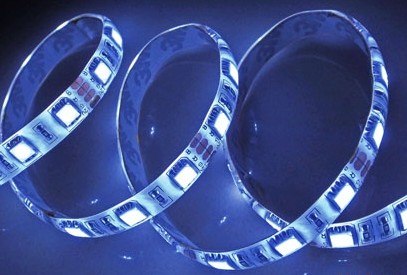
- Flexible LED PCB Boards: Can bend for curved installations, perfect for LED strip PCB boards or wearable lighting.
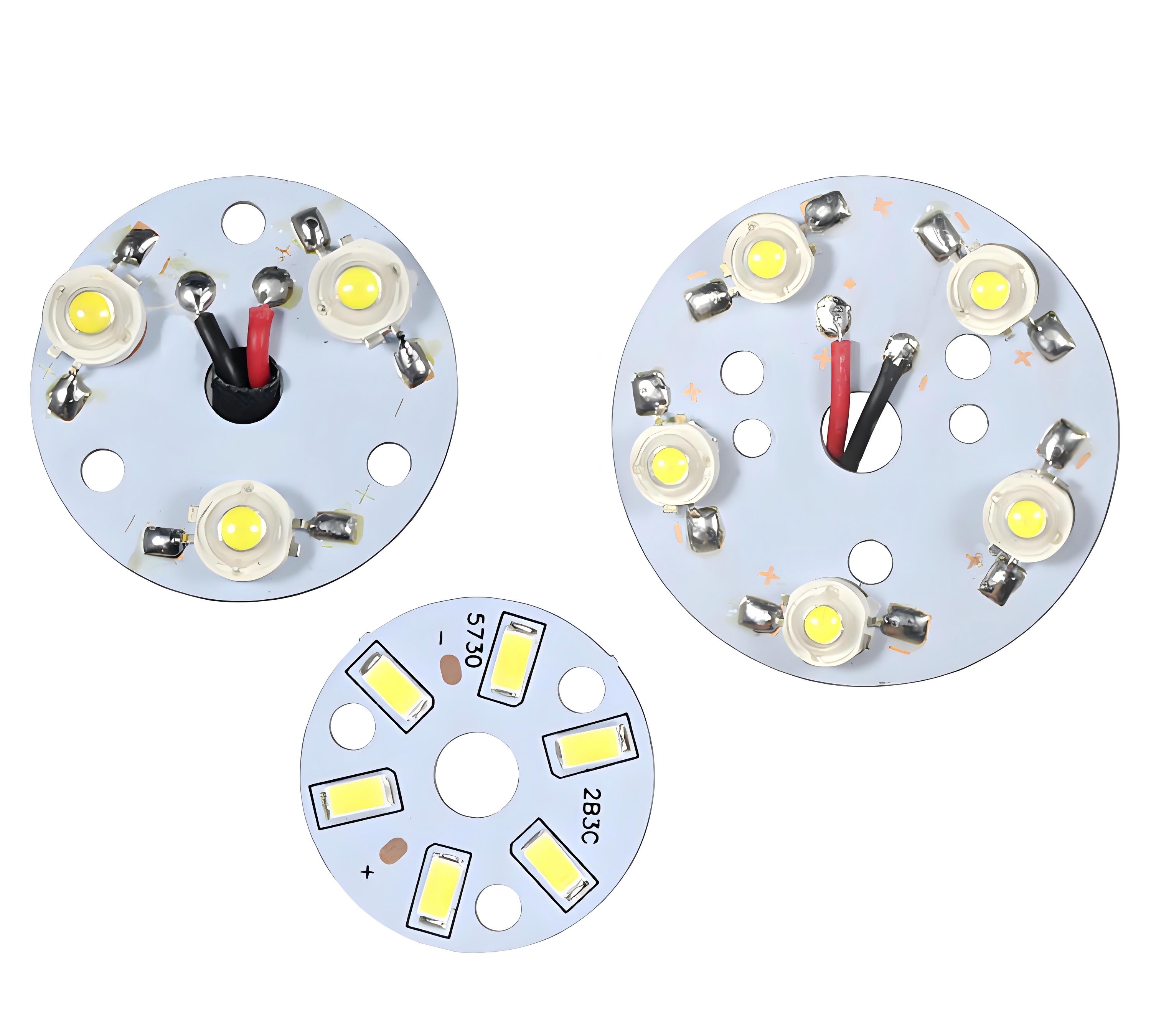
- Metal-Core LED PCB Boards (MCPCB): High heat dissipation, commonly used for LED bulb PCB boards or LED display PCB boards.
LED PCB boards are used across a variety of lighting scenarios including residential and commercial illumination, automotive headlights, industrial lighting, LED display panels, and emergency lighting solutions like LED emergency light circuit PCB boards.
What is SMD LED PCB Board?
SMD stands for Surface-Mount Device, a critical distinction in modern electronics. An SMD LED PCB board refers to a printed circuit board where SMD LEDs are directly mounted and soldered onto the board surface using Surface-Mount Technology (SMT). Unlike traditional through-hole LEDs, which require long leads to pass through the PCB, SMD LEDs are compact, flat, and attach directly to the board, making the board thinner and more space-efficient.
Why SMD is a Big Deal
- Size and Density: SMD LEDs are smaller and lighter, enabling designers to place more diodes on a limited area. This high-density arrangement is essential for LED PCB strips, LED display PCB boards, and high-resolution backlighting. Miniaturization allows slim and lightweight designs for products like LED ceiling light PCB board replacements.
- Performance and Light Quality: SMD LEDs often offer wider viewing angles (120°–180°), higher luminous efficiency, and more color versatility, including RGB LED PCB boards. They provide smooth, even light output for LED light PCB boards in commercial or residential lighting applications.
- Manufacturing and Cost Efficiency: SMD LEDs are ideal for automated assembly with high-speed pick-and-place machines. This reduces labor costs, increases production consistency, and supports cost-effective manufacturing of custom LED PCB boards or LED 12V PCB boards.
- Design Flexibility: The small size allows for complex and compact LED PCB board designs, making it possible to integrate high-power LEDs like LED PCB board 100W or LED PCB board 18W into versatile lighting solutions.
Common SMD LED Types and Identification
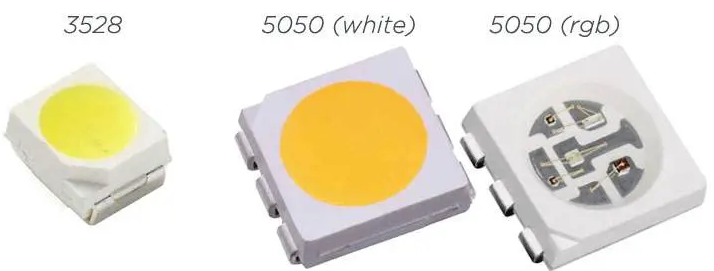
- 2835, 3528: Widely used for general lighting in LED strip PCB boards.
- 5050, 5060: Larger packages for higher brightness or RGB LED PCB boards.
- 3014, 4014: Ultra-thin SMDs for backlighting in LED TV PCB boards or monitors.
- COB (Chip-on-Board): Though not a traditional SMD, it’s a related technology where multiple chips are integrated on a single PCB to form a large, uniform light surface.
Differences Between COB LED Strips and SMD LED Strips
COB and SMD LED strips differ in light efficiency, flexibility, and lifespan.
- Light Quality:
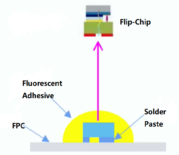
- COB LED strips use chips embedded in a gel-like material, producing a more uniform and soft light.
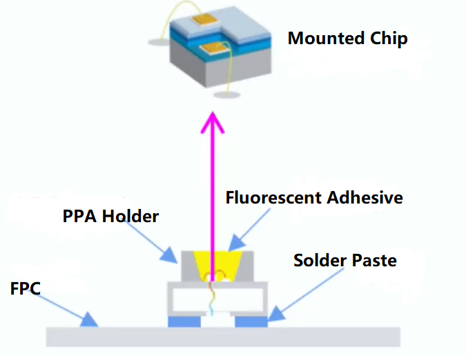
- SMD LED strips have LEDs directly mounted on the PCB. When lit, the individual LEDs are visible, creating a noticeable dot effect. Fewer LEDs increase this dot effect and can create dark spots.
- Flexibility:
- COB strips are more flexible, allowing designers to shape them freely.
- SMD strips can protrude at corners due to the mounted LEDs, limiting design flexibility.
- Thermal Management and Lifespan:
- COB LED strips use flip-chip technology, offering better heat dissipation and longer lifespan.
- SMD LED strips use packaged chips/mounted chips, which have higher thermal resistance and reduced longevity.
Key Applications
- Consumer Electronics: Backlighting for smartphones, tablets, laptops, and LED light PCB boards for compact devices.
- High-End Lighting: Panel lights, LED tube light PCB boards, smart bulbs, and modern automotive lighting systems.
- Display Technology: Indoor and outdoor full-color LED screens, including small-pitch LED display PCB boards (P0.9, P1.2, etc.).
- Decorative Lighting: LED PCB strips, RGB strips, and smart lighting fixtures.
Practical Takeaways for Buyers
- Selection Tips: When choosing SMD LEDs, consider package type (e.g., 2835 for higher efficiency than 3528), color rendering index (CRI), and color temperature.
- Reliability: Since SMD LEDs have exposed solder points, PCB thermal design and production quality are critical to longevity, particularly for high-power applications like aluminium PCB board for LED or LED PCB board 100W setups.
To wrap things up, SMD LED PCB boards are the modern standard in LED technology. The key advantage lies in the surface-mount method, which allows miniaturization, high efficiency, and cost reduction. SMD designs have driven the evolution of LED lighting and displays, from LED ceiling light PCB board replacements to high-resolution LED display PCB boards, making them indispensable in today’s electronics and lighting industry.
What is the Difference: LED PCB Board 100W vs 18W?
The difference between a LED PCB board 100W and an 18W board goes far beyond brightness—it is essentially a battle in thermal management. The 100W design focuses on how to dissipate huge amounts of heat, while the 18W design emphasizes efficient and reliable illumination.
Think of it like this: the 18W board is a family car engine—adequate, reliable, and simple. The 100W board, however, is a high-performance sports car engine—demanding in heat dissipation, power supply, and materials. Their requirements are on completely different scales.
A Side-by-Side Breakdown
- Thermal Management and Heat Dissipation (Core Difference)
- 18W: Heat generation is moderate. Small aluminium PCB boards for LED can dissipate heat through their surface area and simple enclosures (like plastic housings). The thermal design is straightforward.
- 100W: Generates massive heat. Requires large metal heatsinks, often die-cast aluminum, with additional cooling fins. The PCB itself is only part of the thermal system. Poor heat management can lead to immediate LED degradation or failure.
- PCB Design and Materials
- 18W: Standard thermal conductivity of the aluminum or FR4 substrate suffices. Copper traces are relatively simple.
- 100W: High thermal conductivity aluminum or even ceramic substrates are needed. Copper layers must be thick to carry large currents. Circuit layout prioritizes thermal balance to prevent hotspots.
- LED Components and Layout
- 18W: Uses fewer standard SMD LED PCB boards (like multiple 2835 LEDs) to achieve sufficient brightness.
- 100W: Two common approaches:
- High-power COB (Chip-on-Board) LEDs densely integrated.
- Large arrays of mid-power SMD LEDs evenly distributed. Both approaches require advanced LED PCB board design to handle heat.
- Driver Power Requirements
- 18W: Small, low-cost constant-current drivers suffice.
- 100W: Needs high-power, expensive constant-current drivers. Higher input/output voltage and current require components with higher voltage tolerance and current-carrying capacity.
- Safety and Reliability
- 18W: Low risk; failure usually manifests as gradual light decay.
- 100W: High safety risk. Involves high voltage and temperature. Requires superior insulation, fire-resistant materials, IP-rated housings, and multiple protections (over-voltage, over-temperature, short-circuit).
Where They Are Used
- 18W PCB boards: Mainstream for home and commercial lighting—LED ceiling light PCB board replacements, panel lights, desk lamps, and LED PCB strips. Emphasis on cost-effectiveness, compactness, and aesthetics.
- 100W PCB boards: Industrial, outdoor, and specialized lighting—high-mast street lights, industrial floodlights, plant grow lights, stadium lighting, and large searchlights. Priority is maximum luminous output and reliability; size and cost are secondary considerations.
Actionable Advice for Buyers
- Don’t focus solely on wattage: Pay attention to heat dissipation (heatsink design), luminous flux (lumens), and efficiency (lm/W).
- Cost Difference: The total system cost for a 100W solution (PCB + heatsink + high-power driver) is far more than five times that of an 18W board—often tens of times higher.
- Selection Warning: Never use a 100W LED PCB in a confined space or without proper cooling—it risks severe overheating or fire. The 18W boards are much safer and flexible.
All in all, the difference between 100W and 18W LED PCB boards is a classic example of how quantitative changes lead to qualitative transformations. The jump in power requires fundamental changes in PCB materials, layout, heat management, LED selection, and driver design, reshaping the board’s application, safety, and performance. Choosing the right wattage is not just about brightness—it’s about engineering a complete, reliable LED solution.
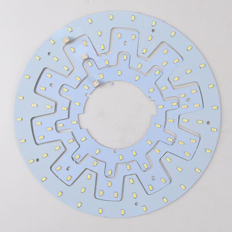
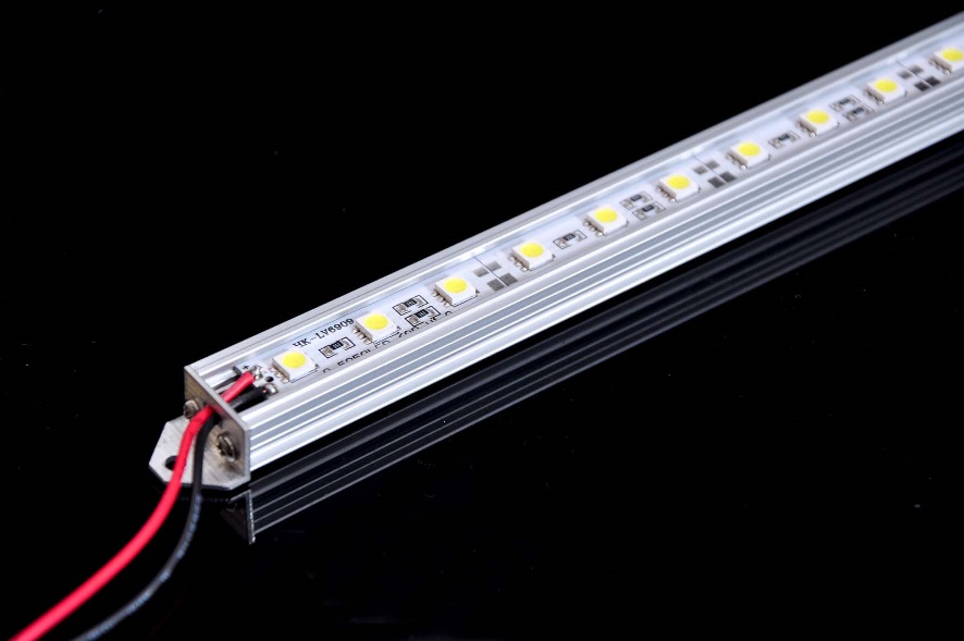
What are the Features of LED Strip PCB Board?
LED strip PCB boards have become a popular choice for modern lighting due to their flexibility, efficiency, and wide design options. From residential decoration to large-scale commercial projects, they combine advanced PCB technology with innovative LED packaging to deliver stable performance and long service life. Understanding their structure, materials, voltage ranges, and chip types is essential for choosing the right solution for different applications.
1. Base Materials of LED Strip PCB Board
- Rigid PCB board: Made with solid PCB substrates, offering better heat dissipation and durability, suitable for high-end lighting applications.
- Flexible FPC board: Lightweight and bendable, ideal for installations in narrow or irregular spaces.
2. Classification by Structure
- Hard LED Strips: Easy to mount, quick heat dissipation, and reliable for projects requiring long service life.
- Soft LED Strips: Ultra-thin and flexible, can be folded or combined freely, widely used in versatile applications.
3. Voltage Options
- High-Voltage Strips: Capable of long-distance lighting (50–100 meters) with a clean appearance, though slightly lower in safety.
- Low-Voltage Strips: Typically 12V/24V, safer for residential and commercial lighting, though limited in length (usually ≤10 meters).
4. LED Chip Specifications
- Popular models include 3528, 2835, 5050.
- Packaging size and chip count affect brightness, power consumption, and cost (e.g., 5050 brightness ≈ 3 times of 3528).
5. Key Features
- Consistent LED spacing for soft and balanced lighting.
- Cuttable design to meet custom length requirements.
- Adhesive backing for quick and simple installation.
- Slim and compact, saving space and fitting multiple scenarios.
6. Application Scenarios
- Ambient and decorative home lighting.
- Commercial displays and advertising light boxes.
- Stage lighting, entertainment venues, and outdoor landscape illumination.
- Automotive interiors and creative DIY projects.
LED strip PCB boards combine versatile designs, safe voltage options, and advanced LED chip technologies to deliver reliable lighting solutions. Whether used in residential decoration, commercial displays, or large outdoor projects, they provide efficiency, ease of installation, and long-lasting performance. For businesses and engineers, understanding the materials, structures, and technical features helps in selecting the most suitable type of LED strip PCB board for specific needs.
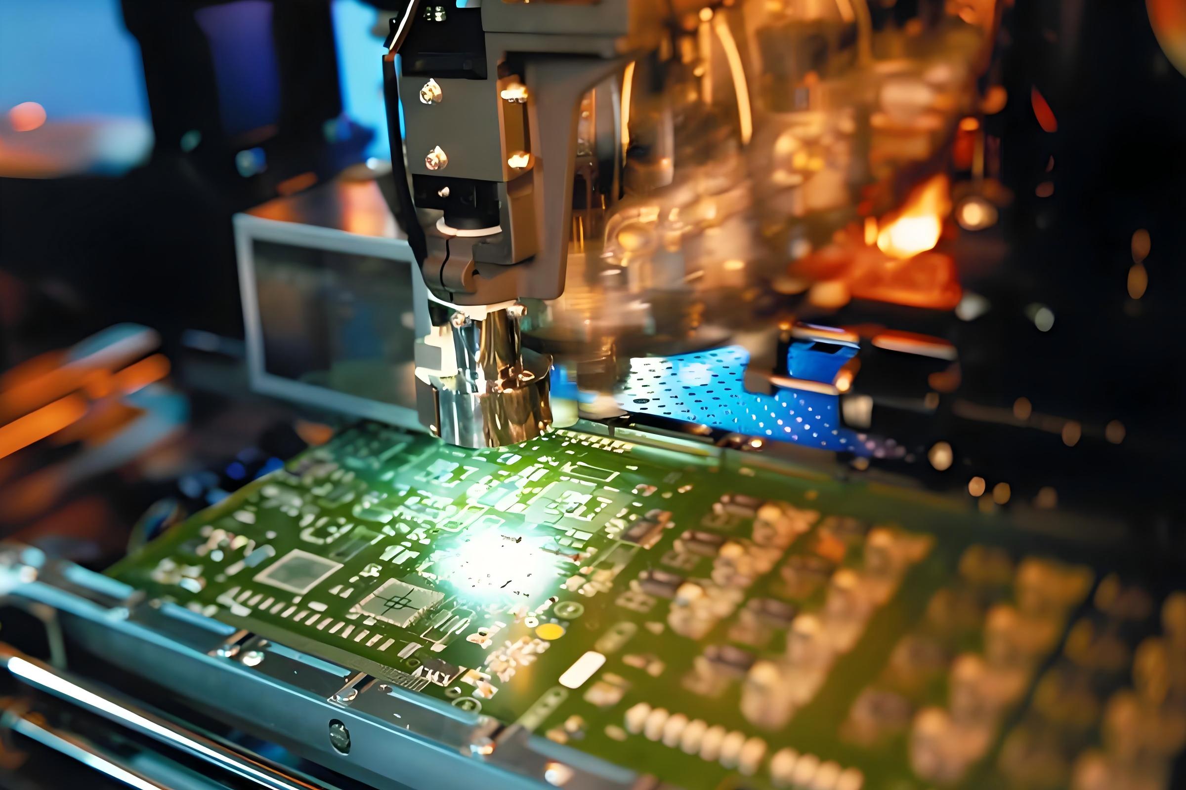
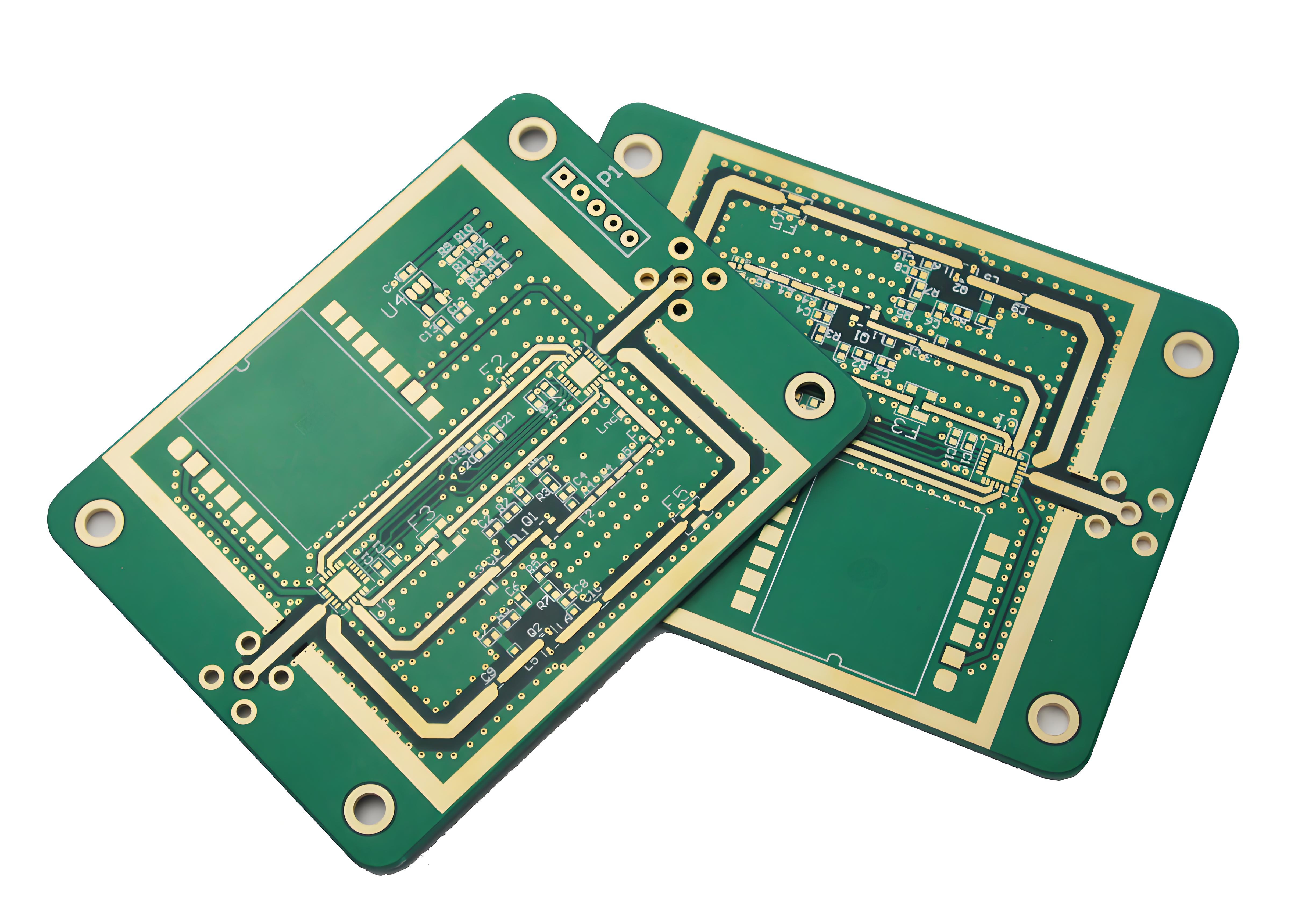
How to Make LED PCB Board?
Making an LED PCB board is a precise process that requires careful attention to circuit design, heat management, and component assembly to ensure stable and reliable lighting performance. While rigid LED boards and flexible LED strips (FPC) differ slightly, the core manufacturing steps are largely similar.
1. Selecting Base Materials
- Rigid PCB Board: Made of FR4 or aluminum substrates, offering excellent heat dissipation and mechanical strength, suitable for high-power LED rigid strips.
- Flexible FPC Board: Thin and bendable, ideal for installation in tight or irregular spaces, used for flexible LED strips.
2. Copper Lamination
- Copper is laminated onto the substrate to form conductive layers.
- Copper thickness is chosen based on current requirements; high-power LEDs require thicker copper to prevent overheating.
3. Circuit Etching
- Unwanted copper is removed to form precise circuit patterns.
- Correct line width and spacing ensure even current distribution and prevent voltage drop or short circuits.
4. Solder Paste Application
- Solder paste is applied to pads to prevent shorts and protect copper traces from oxidation.
- This layer also ensures reliable soldering for LEDs and resistors.
5. Pad Surface Finishing
- Pads can be treated with ENIG, OSP, or other finishes to ensure strong and reliable solder joints.
6. Component Placement
- LED chips, resistors, and other components are placed using automated pick-and-place machines.
- Flexible LED strips commonly use 12, 15, 18, 24, or 30 LEDs per segment.
- Key considerations: correct LED polarity, resistor value, and accurate component positioning to ensure uniform brightness.
7. Reflow Soldering
- The assembly is heated in a reflow oven to melt the solder paste and fix components.
- Temperature control is critical: too low causes cold solder joints; too high can damage FPC or cause warping and solder balls.
8. Inspection and Testing
- Visual Inspection: Check for misaligned components, solder bridges, or shorts.
- Electrical Testing: Verify LEDs operate correctly, current is stable, and voltage meets specifications.
9. Waterproofing (Optional, LED Strip Finished Stage)
Different waterproofing methods vary in encapsulation method and material:
- Epoxy Coating: A thin layer of epoxy is applied to the LED surface; simple but offers limited protection.
- Silicone Tubing: LEDs are inserted into silicone tubes, with ends sealed; flexible and suitable for light water resistance.
- Solid Encapsulation (U-channel + Resin): The strip is placed in a U-shaped channel, then filled with resin; strong structure and good waterproofing.
- Potting (PU or Epoxy Resin): The entire strip is encapsulated in resin, providing maximum weather resistance and protection.
10. Aging, Testing, and Packaging
- Completed PCB or LED strips undergo aging tests to ensure long-term reliability.
- LED strips are typically packaged in 5-meter rolls using anti-static and moisture-proof materials for safe storage and shipping.
To sum up, every stage of LED PCB board production requires precision—from base selection, copper lamination, and circuit etching to component placement and reflow soldering. Flexible strips also require considerations for bendability and space adaptability. Strict manufacturing standards combined with MES system tracking ensure high-quality, reliable LED PCBs widely used in home, commercial, automotive, and decorative lighting applications.
How to Build a LED PCB Board Design Step by Step?
Designing a new LED PCB board requires careful planning and attention to detail. A well-designed board ensures optimal light output, thermal performance, and reliability. Below is a step-by-step guide to LED PCB design:
1. Define Design Goals
Before starting, define the essential goals:
- Target light output (lumens)
- Operating voltage (commonly 12V or 24V)
- Expected lifetime and reliability
- Thermal management requirements
2. Select Materials
Choose base materials based on application:
- Aluminum PCB: Excellent for high-power LEDs, provides superior heat dissipation.
- FR4 PCB: Cost-effective, suitable for low-power LED applications.
- Flexible FPC: Ideal for soft LED strips or irregular shapes.
3. Circuit Layout
Use CAD software to lay out the PCB traces and LED positions:
- Ensure proper spacing between copper traces to prevent shorts and overheating.
- Plan thermal paths for heat dissipation under each LED pad.
- Follow industry-standard design rules for trace width:
For current carrying traces, the IPC-2221 formula is often used:
Trace Width (W) = (I / (k · (ΔT)0.44))1/0.725 where I is current (A), ΔT is allowed temperature rise (°C), k is a constant based on copper thickness.
4. Layer and Drill Planning
Decide the number of layers:
- Single-layer PCB: simplest, low power, low cost.
- Double-layer PCB: standard for most LED boards.
- Multi-layer PCB: for complex designs or higher currents, often 4–6 layers.
Drill locations should match LED lead holes and vias for thermal and electrical connection.
5. Thermal Management
LED performance depends heavily on heat control:
- Use thermal vias under high-power LEDs to conduct heat to the metal core.
- Calculate thermal resistance:
Rθ = (Tjunction_max – Tambient) / Ptotal - Keep copper thickness and pad size sufficient to carry required current.
6. Simulation and Verification
Before fabrication:
- Simulate current flow and temperature rise to detect hotspots.
- Check trace width and spacing using design rule checks (DRC) in CAD software.
- Review LED polarity, pad sizes, and via placements to avoid assembly issues.
7. Prototype and Testing
Build a prototype and test:
- Measure brightness, voltage, and current.
- Verify temperature under load.
- Check electrical continuity and insulation.
- Adjust design as needed before mass production.
8. Final Checks
Ensure the PCB design meets the following:
- All LED pads have correct polarity and spacing.
- Trace width sufficient for current without excessive temperature rise.
- Thermal paths and metal core areas optimized for heat dissipation.
- Layer stackup and drill positions correctly defined.
Following these steps ensures a robust LED PCB design that performs reliably. EBest Circuit (Best Technology) engineers provide professional design review and optimization, reducing redesign costs and improving manufacturing yield.
How to Test LED PCB Board?
Testing an LED PCB board is not just a formality—it’s a critical step to ensure safety, performance, and long-term reliability. Testing ensures LED PCB boards are safe, fully functional, and durable under real operating conditions. It should cover incoming materials, in-process checks, and final inspection, though clients usually focus on final inspection and random sampling to verify quality.
1. Step-by-Step Testing Process
Step 1: Visual Inspection
Objectives:
- Check PCB cleanliness, surface scratches, burns, or mechanical damage.
- Confirm LED orientation, model, and position; no reverse polarity or missing LEDs.
- Inspect solder joints: full, smooth, without cold solder, bridges, or solder balls.
Tools:
- Magnifying glass or microscope (for high-density boards)
- Direct visual inspection
Why it matters: Early detection of physical defects prevents functional failure after power-up.
Step 2: Electrical Performance Testing
Key Tests:
1. Continuity & Short-Circuit Test:
- Use a multimeter to verify all circuits are connected properly.
- Detect shorts or open circuits before powering the board.
2. Insulation & Hi-Pot Test:
- Apply high voltage to check isolation between conductors.
- Critical for safety in high-voltage designs.
3. Power-On Test:
- Apply rated voltage and current.
- Check all LEDs for full brightness; no dead or flickering LEDs.
- Measure brightness, color temperature, and CRI; RGB boards should show consistent color mixing and proper signal response.
Step 3: Optical Performance Testing
Objectives:
- Luminous Flux (Lumens): Ensure total light output meets specifications.
- Color Temperature & Color Coordinates (CCT): Verify light color accuracy (e.g., 2700K warm white, 6000K daylight).
- Color Consistency: Check for batch-to-batch variation; ensure uniform appearance across multiple boards.
Tools:
- Integrating sphere or light measurement equipment
Step 4: Thermal Performance Testing
Objectives:
- Measure LED junction temperature (Tj) under rated load using thermocouples or thermal imaging.
- Calculate thermal resistance (Rθ) and confirm temperature rise is within LED specifications:
Rθ = (Tjunction_max – Tambient) / Ptotal
Where Tjunction_max is maximum allowed junction temperature, Tambient is ambient temperature, and Ptotal is total power.
- Monitor brightness decay after continuous operation (e.g., 30 minutes) to assess thermal stability.
Why it matters: High junction temperatures accelerate LED degradation and reduce lifespan. Controlling thermal performance ensures reliability.
Step 5: Environmental & Reliability Testing
Burn-In Test:
- Continuous operation at rated or slightly higher current for 24–72 hours.
- Screens out early failures (“infant mortality”) before shipping.
Optional Stress Tests (based on application):
- Vibration (for automotive LED boards)
- Thermal cycling or shock (outdoor / IP-rated applications)
- Humidity or waterproof tests
These ensure LEDs meet long-term durability requirements.
2. Practical Guide for Clients
What to request from suppliers:
- Detailed Test Reports / Certificates of Analysis (COA)
- Data for burn-in, optical output, thermal performance, and electrical safety
Sampling Strategy:
- Inspect incoming shipments using standards like AQSL II
- Focus on visual checks, power-on tests, and basic electrical testing
Recommended Tools:
- Essential: Multimeter, adjustable DC power supply, magnifying lens
- Advanced: Thermal camera, integrating sphere
Handling Defects:
- Define Acceptable Quality Limit (AQL)
- Establish clear rejection and return policies
In summary, a rigorous LED PCB testing workflow ensures that boards are safe, functional, and durable. By combining visual, electrical, optical, and thermal inspections with environmental stress testing, clients can confidently verify product quality, reduce field failures, and choose reliable suppliers.
Where to Get an LED Light PCB Board?
Choosing the right supplier is often the hardest step. Some buyers face issues with poor quality, late shipping, or inadequate technical support.
- Quality Assurance: EBest Circuit (Best Technology) solves these pain points with certified systems like ISO 9001, ISO 13485, IATF 16949, and AS9100D. All our manufacturing process are fully compatible with these standard.
- Fast Prototypes: We offer high-quality and quick prototypes. If you have cooperated with us, you will enjoy our strong engineering support. All the prototypes are without MOQ requirements.
- Advanced system and equipment: Using MES traceability, we track each part of the process, giving clients excellent quality in long-term supply. And every year, we will purchase cutting-edge machines to meet the higher volume order needs and the diverse project requirements of different customers.
- Multiple LED PCB Types: We present different lighting PCB types, such as single-layer MCPCB, double-sided MCPCB, double-sided SinkPad PCB, multilayer aluminum PCB, COB PCB, IMS PCB, and others.
In closing, whether it is an LED PCB board 12V, an LED PCB Strip, or custom LED PCB, EBest Circuit (Best Technology) delivers both small and large runs without delay.
What are the Applications of LED PCB Boards?
LED PCB boards are no longer just for basic lighting. They now enable precision, flexibility, and energy savings across virtually every sector that requires controlled light. From industrial lamps to high-tech displays, LED boards drive innovation and efficiency, influencing both technical choices and commercial strategy.
1. Detailed Applications by Sector
1.1 Lighting Applications
General & Commercial Lighting:
Indoor panel lights, downlights, bulbs, tubes, industrial and commercial luminaires, and street lamps.
Key considerations: cost efficiency, luminous efficacy, lifespan, and color rendering (CRI).
Specialty Lighting:
- Automotive Lighting: DRLs, headlights, tail lamps, interior ambient lights.
Focus: reliability, vibration resistance, thermal performance, automotive certifications (e.g., ISO 16750). - Medical Lighting: surgical shadowless lamps, dental lamps, UV sterilization lights, phototherapy devices.
Focus: flicker-free operation, precise color temperature, sterilization efficiency, safety compliance. - Agricultural Lighting: plant growth LEDs targeting specific spectra (red and blue).
Focus: spectral accuracy, waterproofing, high PPF/PPFD for plant growth efficiency.
1.2 Display & Backlight Applications
- Information Displays: outdoor billboards, stadium screens, traffic signage, financial tickers.
Focus: high brightness, fast refresh, weatherproofing, long-distance visibility. - Consumer Electronics Backlight: LCD TVs, monitors, laptops, tablets.
Focus: thin form factor, uniform light distribution, advanced Mini/Micro LED technologies. - High-End Commercial Displays: indoor small-pitch LED screens for command centers, meeting rooms, broadcasting.
Focus: pixel density, color consistency, low brightness/high gray performance.
1.3 Signaling & Indication
- Traffic Signals: traffic lights, railway indicators.
Focus: ultra-reliable operation, brightness, precise wavelength for visibility and compliance. - Status Indicators: appliances, industrial equipment, network routers.
Focus: compact size, long lifetime, low power consumption.
1.4 Emerging & Innovative Applications
- UV/IR LEDs: UV for curing (3D printing, nail art, ink printing) and sterilization; IR for night vision and facial recognition.
Focus: wavelength-specific power, effective thermal management. - Wearables & Smart Devices: smart wristbands, health monitors, flexible luminous textiles.
Focus: flexible PCB, low power consumption, lightweight design. - Automotive & Smart Transportation: beyond lighting, including LiDAR and optical sensing.
Focus: precision optics, high-speed pulse performance.
2. Insights and Decision-Making Guide
Technical Requirements Comparison Across Applications:
- Thermal Management: low for status indicators, extreme for high-power street lights and UV curing devices.
- PCB Type Selection: rigid (industrial/street lights), FPC (flexible strips), MCPCB (metal-core for automotive), ceramic (UV/IR for heat-intensive applications).
- Performance Priorities: brightness, color accuracy, lifespan, cost – weighted differently per application.
Communicating with Suppliers:
Do not just say “I need a LED board.” Specify the end-use scenario (e.g., “outdoor plant growth light”), so suppliers can recommend power rating, spectral design, IP rating, and thermal solutions accurately.
Trends and Future Outlook:
- Mini/Micro LED: driving next-generation displays, requiring high PCB precision.
- Smart Lighting & IoT Integration: higher integration with sensors and controllers.
- Efficiency & Sustainability: ongoing improvements in luminous efficacy and environmentally friendly materials.
To conclude, LED PCB boards serve as a strategic technology platform across multiple sectors. By mapping applications, understanding technical requirements, and analyzing business value, clients can make informed decisions on design, procurement, and market opportunities. This approach helps identify where and why LED PCBs are used, enabling optimized product strategies and competitive advantage.
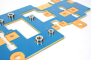
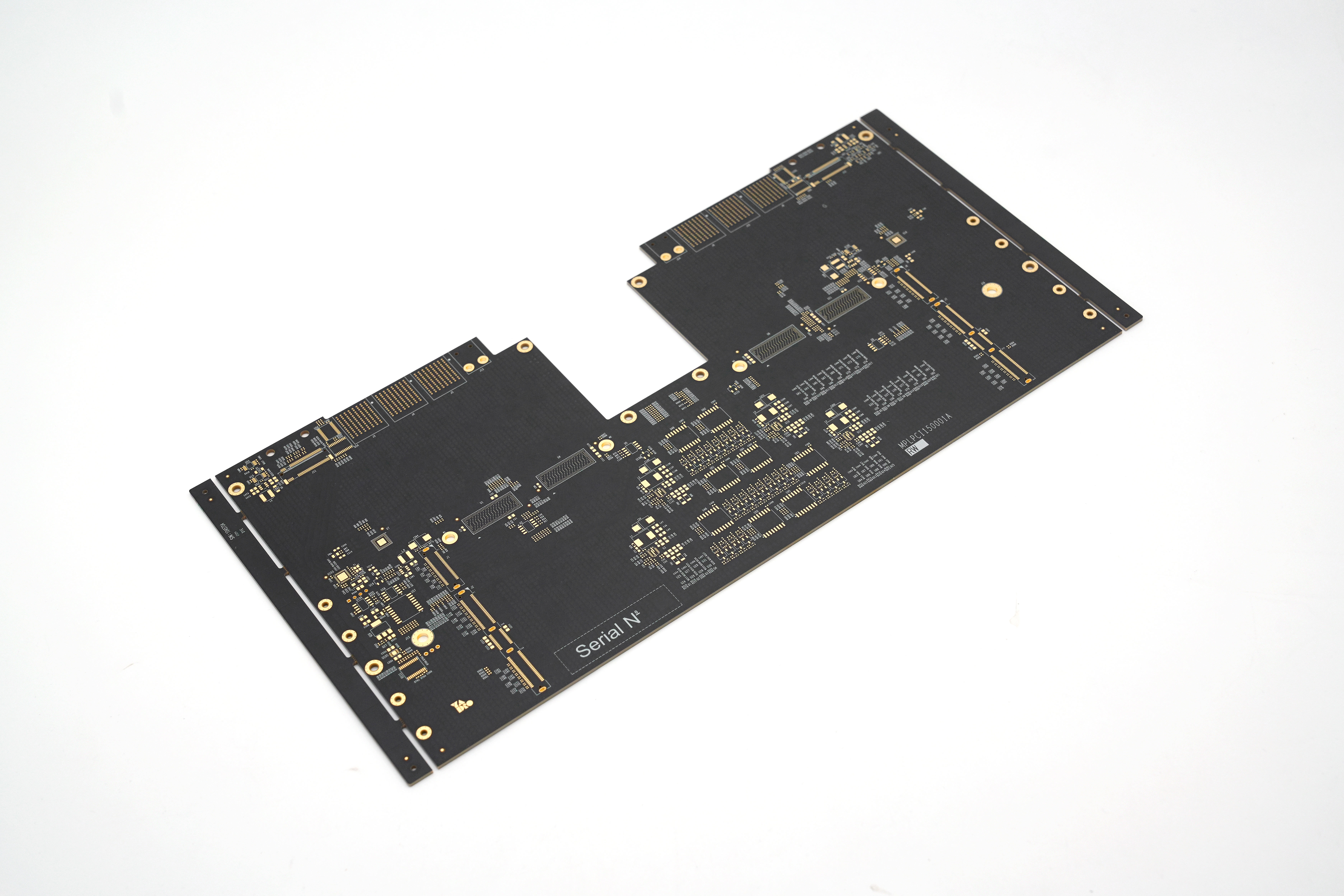
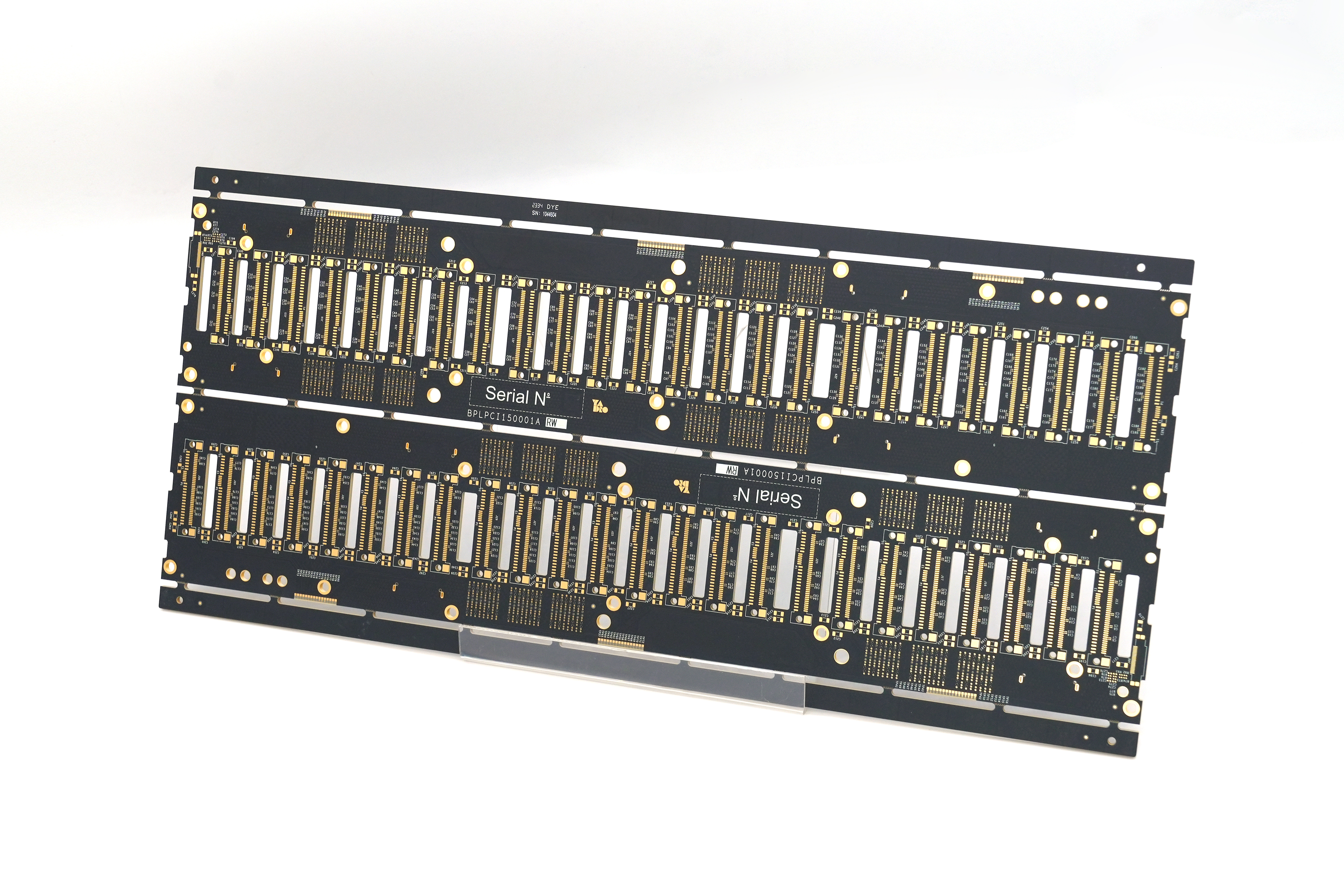
Case of PCB Light Board in EBest Circuit (Best Technology)
Here are some cases EBest Circuit (Best Technology) completed for our customers. These LED PCB boards are widely applied in different lighting projects, from outdoor high-power lamps to indoor decorative lights. Their design and performance directly support brightness, stability, and long lifespan in real applications.
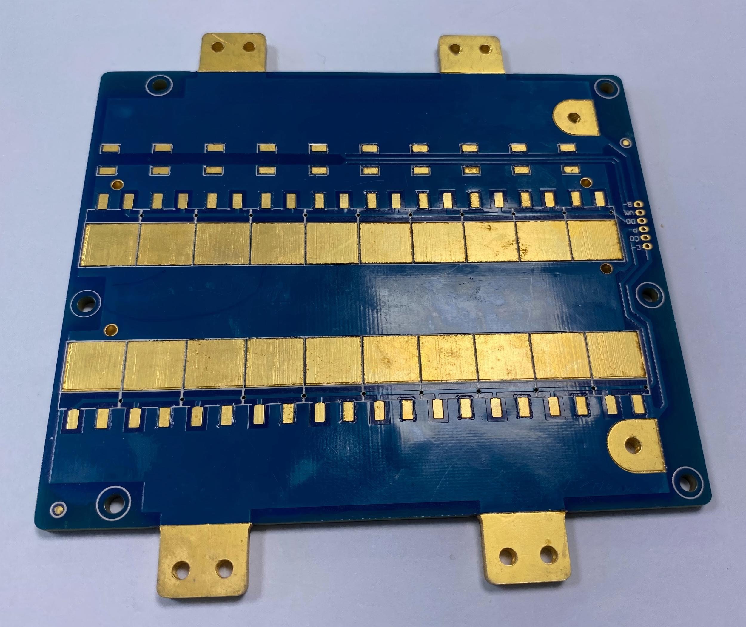
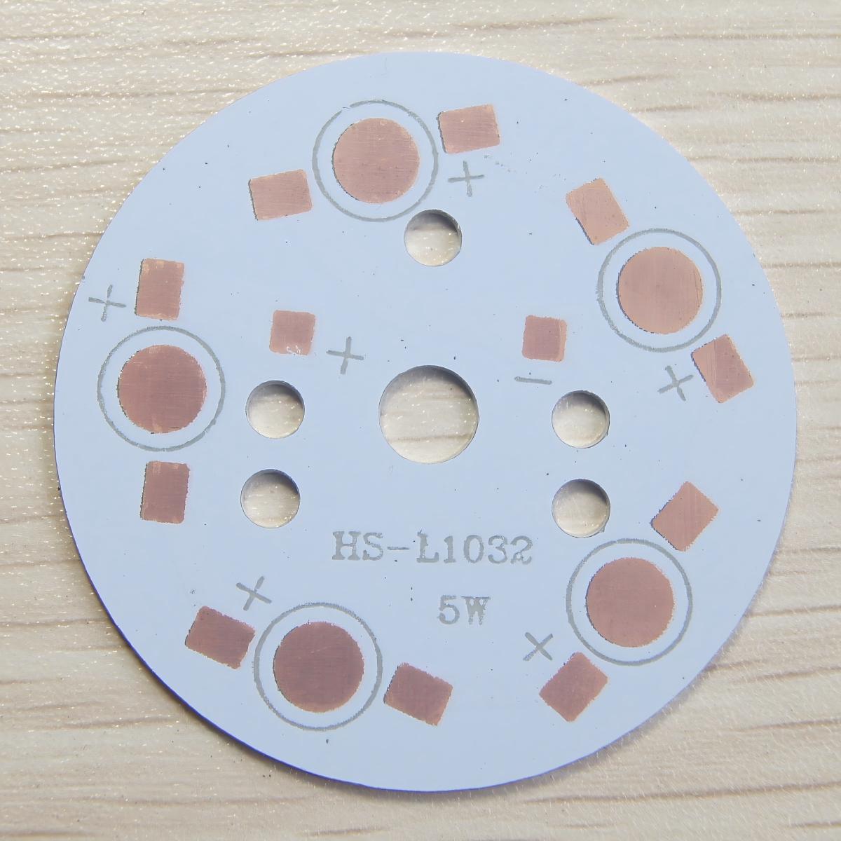
Double-Sided Aluminum PCB
- Finished board thickness: 1.6mm±10%;
- Thermal conductivity: 3W;
- Copper thickness: 1OZ;
- Solder mask: Black with white legend;
- Surface finish: Lead-free HASL;
This type of PCB is commonly used in high-power LED floodlights, street lamps, and stadium lights. Its double-sided structure supports complex circuit routing, while the aluminum base helps manage high thermal loads. In outdoor lighting projects, such as highway lighting or public square illumination, these boards provide both durability and efficiency.
Single-Sided Double-Layer Copper PCB
- Copper base thickness: 1.3mm;
- Copper thickness: 1/1OZ;
- Thermal conductivity: 3W/m.k;
- Finished board thickness: 1.60mm±10%;
- Solder mask: Black with white legend;
- Surface finish: OSP;
This copper-based PCB is often chosen for LED power supply modules, industrial lighting fixtures, and high-brightness spotlights. The excellent conductivity of copper provides stable current flow, which is important in commercial lighting systems, stage spotlights, and smart control LED panels. It delivers both high brightness and reliable performance under continuous use.
Single-Sided Double-Layer Aluminum PCB:
- Aluminum base thickness: 1.50mm;
- Copper thickness: 0.5/0.5OZ;
- Thermal conductivity: 3W/m.k;
- Finished board thickness: 1.85mm±10%;
- Solder mask: Black with white legend;
- Surface finish: OSP;
This board is suitable for LED panel lights, downlights, tube lights, and automotive interior lamps. The aluminum base ensures strong heat dissipation, while the dual copper layers maintain circuit stability. It is widely used in office ceiling lighting, residential decorative lamps, and car dashboard backlight systems, where energy efficiency and uniform brightness are required.
In a nutshell, LED PCB boards are more than just carriers of light. They balance power, heat, and cost in ways that define product success. Yet, buyers often face real pain points: lack of design support, poor heat control, or unreliable supply. EBest Circuit (Best Technology) meets these challenges with certified processes, strong engineering, and a customer-first mindset. By offering LED PCB board design advice, reliable testing, and professional service through all process, we give clients the trust they need. A warm welcome to get in touch with us via sales@bestpcbs.com for a creative solution.