PCB manufacturing in China holds a dominant global position, with China accounting for more than half of the world’s total production volume. This leadership is supported by a complete and highly sophisticated ecosystem, spanning raw material suppliers, advanced equipment manufacturers, skilled engineering talent, and large-scale manufacturing capacity. The strong cluster effect in regions such as the Pearl River Delta and the Yangtze River Delta enables exceptional supply chain efficiency and cost advantages.
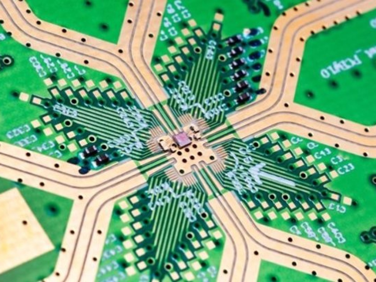
For high-frequency boards, which require specialized materials like Rogers or Teflon and extremely precise process control, China hosts numerous manufacturers that have invested heavily in the requisite technology and expertise. While the market is vast, finding a reliable partner for such critical applications requires careful evaluation of technical capability, quality systems, and project management rigor within the PCB manufacturing in China landscape. Don’t hesitate to contact us via sales@bestpcbs.com if you require any PCB quote.
Top 10 PCB Manufacturers in China
The following table lists some of the leading PCB manufacturers in China with capabilities for high-frequency and high-performance boards.
| Company Name | Process Capability (HF Boards) | Key Advantages |
|---|---|---|
| Shennan Circuits (SCC) | HDI, RF/Microwave | R&D strong, high reliability |
| WUS Printed Circuit | RF, Backplane | Complex boards expert |
| Kinwong Electronics | High-Thermal, HDI | Automated production |
| EBest Circuit (Best Technology) | RF/Microwave, High-Speed, HDI | Strong engineering, fast delivery |
| DSBJ (Fastprint) | HDI, IC Substrate | Quick-turn specialist |
| Aoshikang (AKM) | RF, Rigid-Flex | Broad capability |
| Suntak Technology | HDI, Rogers/Teflon | Communication-focused |
| Victory Giant | High Layer, HDI | Strong telecom reliability |
| Jingwang Weidian | RF, Rigid-Flex | Engineering-driven |
| Ellington Electronics | RF, HDI | Automotive & telecom strength |
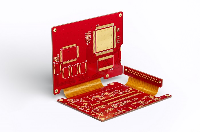
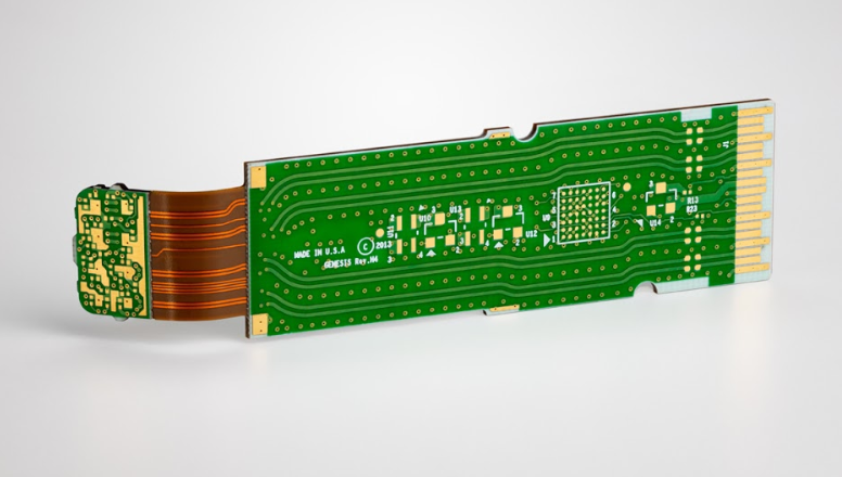
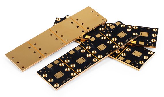
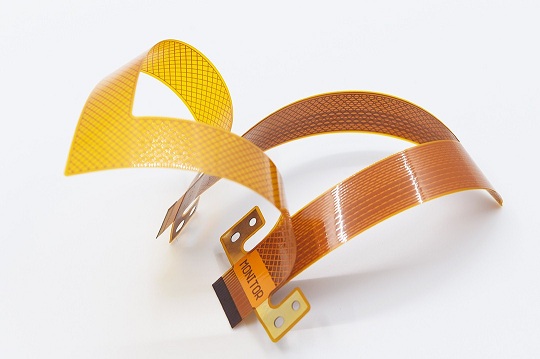
EBest Circuit (Best Technology) Co., Limited, founded in 2006, is a direct Chinese PCB manufacturer with full in-house production and certifications including ISO 9001, ISO 13485, IATF 16949 and AS9100D. We provide a wide range of PCBs such as metal core PCBs for LED thermal management, ceramic PCBs for 5G, RF and power electronics, standard rigid and multilayer PCBs for consumer and industrial devices, and special PCBs including HDI, IC substrate, heavy copper, thin PCB and impedance control designs.
All products support full customization and comply with RoHS and REACH. With a monthly capacity of 260,000 sq. ft and over 1,000 different boards delivered each month, EBest Circuit (Best Technology) is committed to quality, innovation and fast turnaround, offering urgent PCB delivery within 24 hours. Pls feel free to get in touch with us via sales@bestpcbs.com or +86-755-2909-1601 for any PCB manufacturing and PCBA demands.
Core Pain Points When Working With Any PCB Manufacturer in China
Engaging a PCB manufacturer in China offers immense benefits but comes with distinct challenges. Awareness of these common pain points is crucial for successful collaboration, especially for sensitive products like high-frequency boards.
- Material Sourcing and Authenticity: Ensuring the use of certified, high-quality, and authentic high-frequency laminates (e.g., Rogers, Taconic) can be a concern, as some manufacturers may propose unverified substitutes to cut costs.
- Communication and Language Barriers: Technical misunderstandings can arise due to language differences, time zones, and cultural nuances in communication styles, potentially leading to specification errors.
- Quality Consistency in High-Mix Volumes: Maintaining absolute consistency in critical parameters (like dielectric constant and loss tangent) across batches, especially when switching production lines or operators, is a constant challenge.
- Intellectual Property (IP) Protection: Despite improving laws, concerns about design IP and process know-how security persist, requiring robust NDAs and careful information sharing practices.
- Limited Proactive Engineering Support: Some manufacturers operate primarily as “order takers” rather than providing proactive Design for Manufacturability (DFM) feedback, which is essential for optimizing complex high-frequency designs.
- Supply Chain Transparency: Visibility into the sub-tier supply chain (e.g., chemical suppliers, laminate vendors) can be limited, making it harder to audit overall quality control and ethical sourcing.
Proactively addressing these pain points through clear contracts, thorough audits, ongoing communication, and building a relationship-based partnership is key to mitigating risks and ensuring project success with your chosen PCB manufacturer in China.
How to Evaluate Production Capabilities of a PCB Board Manufacturer in China?
A thorough assessment of a PCB board manufacturer in China goes beyond basic quotes. For high-frequency boards, due diligence must focus on technical and process mastery.
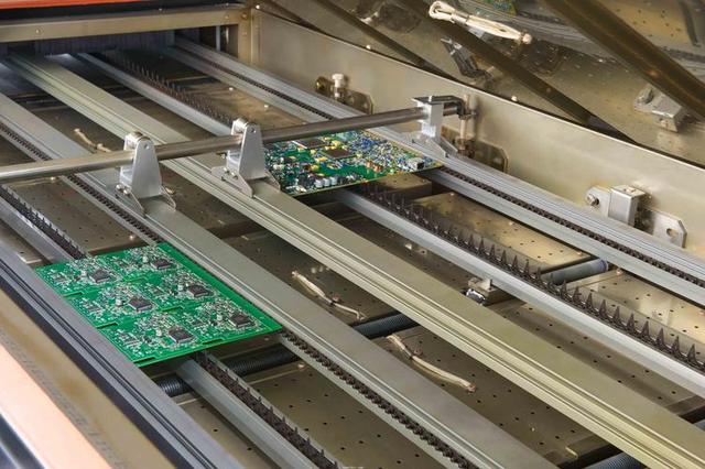
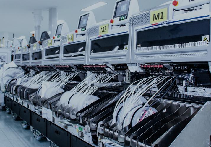
- Audit Equipment and Facility: Verify the presence of advanced, well-maintained equipment suitable for HF boards: laser direct imaging (LDI), vacuum pressing, plasma desmear, controlled impedance testing, and high-precision lamination presses.
- Review Certifications and Process Controls: Look for relevant certifications (e.g., IATF 16949, AS9100, UL) and ask about their Statistical Process Control (SPC) and quality management systems for critical parameters.
- Request Product Portfolio and References: Examine past production samples, especially for similar high-frequency or high-speed applications. Request client references in your industry.
- Assess Engineering and DFM Expertise: Engage their engineering team in a technical discussion. Evaluate their ability to provide insightful, proactive DFM feedback on your design files.
- Evaluate Prototyping Process: Understand their quick-turn prototyping flow, including engineering review time, material stocking, and dedicated prototype lines. This reflects agility and priority for NPI (New Product Introduction).
- Test Their Material Expertise: Question them deeply on material properties, processing guidelines for different high-frequency laminates, and their relationships with authorized material distributors.
By systematically investigating these areas, you can move beyond surface-level claims and gain a true understanding of the technical competence and reliability of the PCB board manufacturer in China you are considering.
Key Factors for Assessing Delivery Speed From PCB Manufacturers in China
Delivery time is a critical metric. For PCB manufacturers in China, speed is influenced by multiple factors beyond just the “production lead time” quoted.
- Material Inventory and Sourcing Time: Confirm the availability of your specified high-frequency laminate in their stock. Sourcing specialty materials can add weeks if not in inventory.
- Engineering Review Efficiency: A swift, thorough, and collaborative engineering/DFM feedback cycle (typically 24-48 hours) prevents delays and avoids multiple revision spins.
- Prototype vs. Volume Production Lines: Leading manufacturers have dedicated, expedited lines for prototypes. Ensure your prototype won’t be queued behind large volume orders.
- Process Complexity Impact: Understand how your board’s specs (tight tolerances, via fills, sequential lamination, special finishes) add to the standard production cycle. A transparent manufacturer will detail this.
- Testing and Validation Time: Factor in time for electrical testing, impedance testing, and any required reliability testing (e.g., thermal cycling). Complex testing requirements extend lead times.
- Logistics and Shipping Pre-Arrangement: Discuss and pre-arrange shipping methods (air vs. sea) and customs documentation to avoid last-minute logistical delays.
A realistic and reliable delivery timeline from PCB manufacturers in China is built on transparent communication about each of these stages, not just a single promised date. Partner with manufacturers who provide clear, stage-by-stage tracking.
Major Industry Challenges Faced by the PCB Manufacturing in China Market
While leading global PCB manufacturing in China, the industry itself navigates a complex set of internal and external pressures that shape its evolution and competitive landscape.
- Intense Price Competition and Margin Pressure: The market is highly saturated at the low to mid-range, leading to fierce price wars that squeeze margins and can compromise quality if not managed.
- Rising Labor and Operational Costs: Increasing wages, land costs, and stricter environmental regulations, especially in coastal regions, are eroding the traditional cost advantage.
- Dependency on Advanced Equipment and Materials: High-end production, especially for HF and IC substrates, relies heavily on imported equipment (from Europe/Japan) and specialty raw materials, impacting supply chain security and costs.
- Technological Gap in Cutting-Edge Segments: While strong in many areas, a gap still exists compared to global leaders in the most advanced technologies like ultra-HDI, advanced substrate packaging (e.g., FC-BGA), and certain semiconductor-level processes.
- Environmental Compliance and Sustainability Pressures: Adhering to increasingly stringent national and international environmental regulations (e.g., waste treatment, carbon footprint) requires significant and ongoing investment.
- Global Geopolitical and Trade Tensions: Tariffs, trade restrictions, and “de-risking” trends can disrupt supply chains, affect export markets, and complicate technology transfer.
The future of PCB manufacturing in China hinges on the industry’s ability to move up the value chain, innovate in advanced technologies, embrace automation for efficiency, and successfully navigate the sustainability and geopolitical challenges of the global market.
Practical Recommendations for Choosing the Best PCB Manufacturer in China
Selecting the right partner is strategic. Follow these actionable steps to identify and qualify the best PCB manufacturer in China for your high-frequency board needs.
- Define Your Requirements Precisely: Create a detailed specification document covering material stack-up, tolerances, electrical performance (impedance, loss), testing requirements, and certifications needed.
- Prioritize Specialization Over Generalization: Seek manufacturers with a proven track record and dedicated production lines for high-frequency/RF/microwave boards, not just general PCB producers.
- Conduct a Rigorous Site Audit (Virtual or In-Person): If possible, audit the facility. Assess cleanliness, equipment, operator discipline, and quality control checkpoints on the production floor.
- Start with a Prototype Project: Before committing to volume, place a small prototype or pilot-run order. This is the best way to evaluate real-world performance on quality, communication, and timing.
- Evaluate the Engineering Team Interaction: The quality of technical communication during the RFQ and DFM stage is a leading indicator of future support. Responsive, knowledgeable engineers are invaluable.
- Clarify IP Protection and Contract Terms: Ensure a strong Non-Disclosure Agreement (NDA) and clear contract terms covering quality standards, liability, delivery schedules, and payment terms.
- Verify Supply Chain and Material Traceability: Request evidence of authorized distribution for the high-frequency materials you specify to guarantee performance and authenticity.
- Consider Long-Term Partnership Potential: Look for a manufacturer interested in building a relationship, willing to grow with your business, and invest in processes that support your future technology roadmap.
Finding the best PCB manufacturer in China is a diligent process of matching your specific technical and business needs with a manufacturer’s proven capabilities and cultural alignment for partnership, moving beyond price as the sole deciding factor.
Why Select EBest Circuit (Best Technology) for Your PCB Manufacturing in China?
Choosing the right partner for PCB manufacturing in China is critical when your project involves high-frequency, multilayer, HDI, or special-material boards. With thousands of PCB manufacturers in China—ranging from small prototype shops to the largest PCB manufacturer in China—it becomes essential to identify a supplier that offers consistency, advanced engineering, and predictable project control.
EBest Circuit (Best Technology) stands out as a trusted PCB manufacturer in China, delivering stable performance across RF, microwave, high-speed digital, and rigid-flex applications. Whether you require a 4 layer PCB manufacturer in China, 10–20 layer PCB manufacturer in China, 22–36 layer PCB manufacturer in China, or a specialized antenna PCB manufacturer in China, our team supports you with end-to-end technical capability.
1. Proven Expertise Across High-Complexity PCB Types
- EBest Circuit (Best Technology) is not only known as a high frequency PCB manufacturer in China, but also as a reliable partner for RF, microwave, and antenna systems, making us competitive among the top PCB manufacturers in China.
- We routinely manufacture Rogers, Taconic, Teflon/PTFE, and hybrid stack-ups for industries requiring precision and reliability.
2. Full Capability Coverage: From Simple to Ultra-Complex Multilayer Boards
- We support a wide range of structures—from 4 layer PCB manufacturer in China services to 22–36 layer PCB manufacturer in China high-density stack-ups.
- Our facilities specialize in blind/buried vias, via-in-pad, HDI, sequential lamination, and impedance-controlled routing, positioning us strongly among HDI PCB manufacturers in China.
3. Dedicated Support for Industry-Specific Applications
EBest Circuit (Best Technology) services multiple vertical markets as a:
- 5G base station PCB manufacturer in China
- aviation PCB manufacturer in China
- medical equipment PCB manufacturer in China
- drone PCB manufacturer in China
- industrial equipment PCB manufacturer in China
We understand compliance, reliability, and documentation control required by these industries.
4. Strong Material Expertise Including Rogers, Taconic, and High-TG FR4
- As a leading rogers PCB manufacturer in China and taconic PCB manufacturer in China, our team understands DK/DF control, copper roughness, press cycles, and routing rules needed for demanding RF layouts.
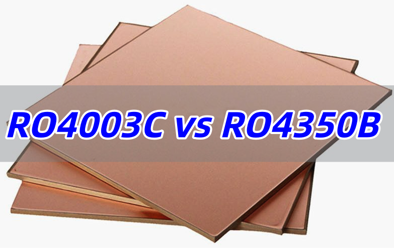
- We support Rogers 4350B, 5880, 3003, TMM series, and Taconic TLY/RT/CE grades.
5. Precision Manufacturing for Antenna, RF, and Microwave Boards
- If you require an antenna in PCB manufacturer in China, RF PCB manufacturer in China, or microwave PCB manufacturer in China, our engineering team provides build-ready design reviews, stack-up optimization, and accurate impedance modeling to enhance RF performance.
6. Reliable Prototype-to-Mass Production Workflow
- Unlike many suppliers focused solely on volume production, EBest Circuit (Best Technology) excels in quick-turn prototypes and stable ramp-up to mass production.
- This makes us ideal for custom PCB manufacturing in China, PCB prototype manufacturer in China, and complex R&D applications.
7. Advanced Equipment Ensuring Consistent Quality
Our factory utilizes LDI, vacuum lamination, plasma desmear, AOI, flying-probe test, and impedance analyzers. This supports precision builds required by:
- multi layer PCB board manufacturer in China
- high-speed high-frequency PCB board manufacturer in China
- PCB high frequency board processing manufacturer in China
8. Strong Engineering Communication and Project Management
- Technical misunderstandings are common when working with a PCB board manufacturer in China, especially on RF and HDI designs.
- Our bilingual engineering team provides proactive communication, weekly updates, and full DFM/DFT reports.
9. One-Stop PCB + Assembly Capability
- As a full PCB and assembly manufacturer in China, we provide SMT, DIP wave soldering, reflow, functional testing, and turnkey BOM sourcing.
- This makes EBest Circuit (Best Technology) a preferred partner for clients needing assembled PCB manufacturer in China service.
Selecting the right partner for PCB manufacturing in China requires more than comparing prices. You need a supplier with proven engineering depth, high-frequency expertise, strong process control, and dependable communication. EBest Circuit (Best Technology) combines all these strengths, making us one of the best PCB manufacturers in China for RF, microwave, HDI, multilayer, antenna, and high-reliability applications. With advanced equipment, skilled engineers, and a customer-focused mindset, we deliver consistent quality across prototypes and mass production.
For companies seeking a trustworthy best PCB manufacturer in China, EBest Circuit (Best Technology) provides long-term value and technical confidence for your most challenging PCB projects. For more information or if you would like to send us any inquiry, please send us an email through the contact form at the bottom of our Contact US Page.
FAQs
Who is the largest PCB manufacturer in the world?
- Zhen Ding Technology Holding Limited (ZDT), also known as AT&S, is frequently ranked as the world’s largest PCB manufacturer by revenue, particularly strong in high-density interconnect (HDI) and substrate-like PCBs for the smartphone and semiconductor sectors.
What is the best PCB manufacturer?
- There is no single “best” manufacturer globally. The best choice is entirely application-dependent. For consumer electronics, it might be Unimicron or Compeq; for high-frequency communication, Shennan Circuits or EBest Circuit (Best Technology); for flexible circuits, it could be Flexium or MFLEX.
Who is the best manufacturer of PCB in China?
- For high-frequency and high-complexity boards, Shennan Circuits Co., Ltd. (SCC) is widely regarded as one of the best domestic PCB manufacturers in China, known for its advanced technology, scale, and service to top-tier clients. For a broader market leadership, EBest Circuit (Best Technology) is a top contender.
Who is the largest PCB supplier?
- The term “supplier” can refer to a manufacturer or a distributor. The largest manufacturer is Zhen Ding Tech (AT&S) as noted. One of the largest global distributors of PCBs and related services is companies like Benchmark Electronics or SIIX, though many OEMs source directly from large manufacturers.
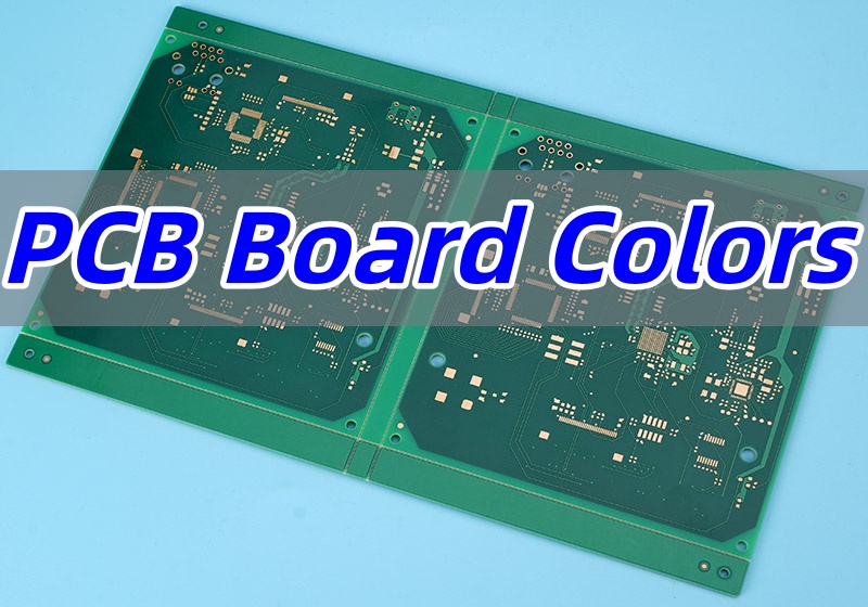
What is the most expensive PCB color?
- While color has a minimal impact on electrical performance, it can affect cost in production. White is often considered the most expensive or challenging color for solder mask due to its lower contrast for AOI (Automated Optical Inspection) and potential to show impurities more easily, potentially requiring more stringent process control.
What are the global PCB manufacturers ranking?
- The global PCB manufacturer ranking by revenue (top 5-10) is relatively stable year-to-year. A typical recent top tier includes (in no strict order): Zhen Ding Tech (AT&S, China/Austria), Unimicron (Taiwan), TTM Technologies (US), Compeq Manufacturing (Taiwan), Shennan Circuits (China), EBest Circuit (Best Technology) (China), and Nippon Mektron (Japan). Official rankings are published annually by industry associations like N.T. Information or Prismark.