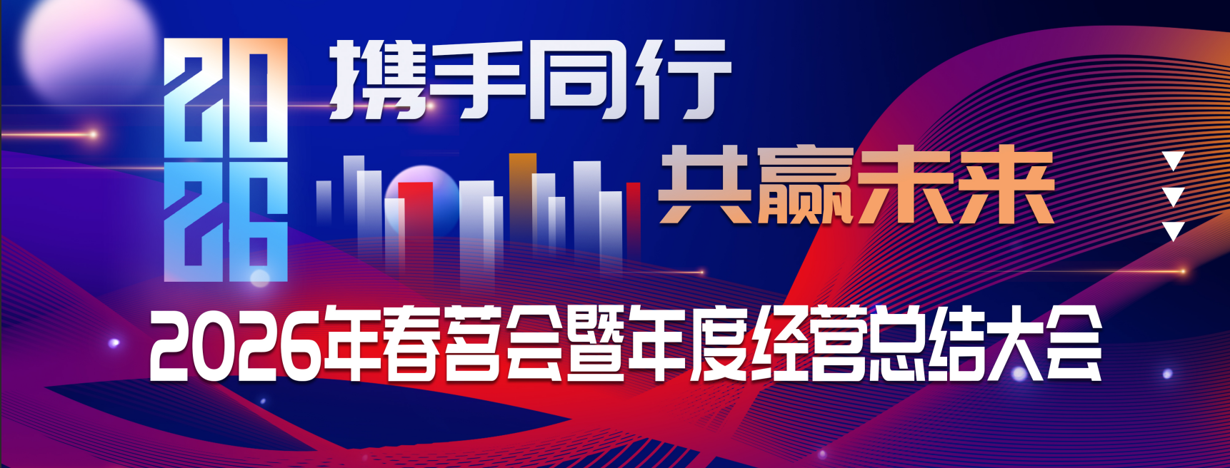
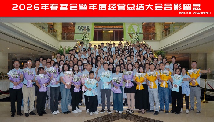
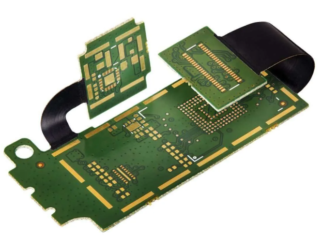
On March 21, EBest Circuit held its 2026 Spring Banquet, bringing employees together to reflect on the past year, recognize team contributions, and look ahead to the company’s goals for 2026.
More than a seasonal gathering, the event was an important annual moment for review, alignment, and team connection. It reflected EBest Circuit’s commitment to open communication, continuous improvement, and a company culture built on collaboration, dedication, and shared growth.
Looking Back, Moving Forward
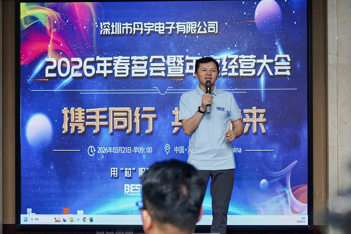
The event opened with remarks from General Manager Peter, who reflected on the company’s journey through 2025 and shared his outlook for the year ahead. In his speech, he recognized the hard work and commitment shown by employees across all departments and expressed confidence in the company’s future development.
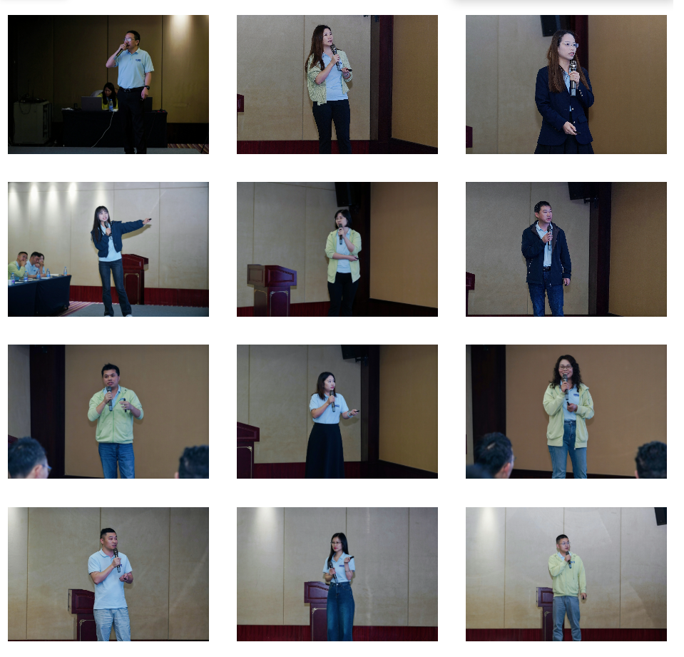
Following his remarks, department leaders presented their annual reviews, covering key results, challenges, lessons learned, and priorities for 2026. These presentations gave the team a clear view of the company’s progress and helped align everyone around the goals and direction for the coming year.
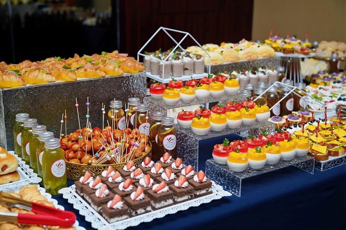
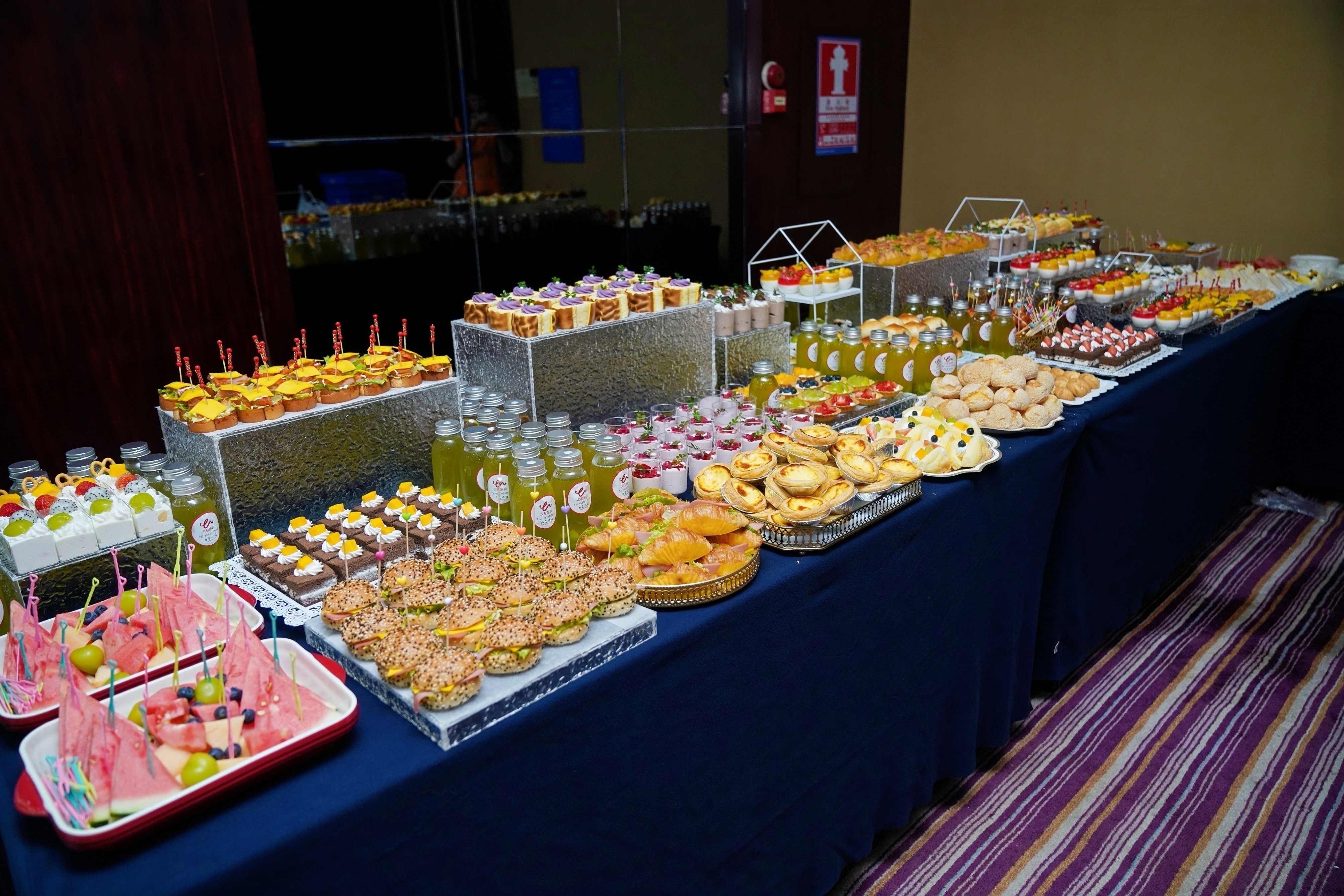
A short afternoon tea break added a warm and relaxed touch to the event, giving employees time to connect and recharge. It also reflected the people-focused culture that remains an important part of EBest Circuit’s identity.
Recognizing Commitment
In the second half of the event, Peter returned to summarize the discussions and reinforce the company’s strategic priorities for 2026. He encouraged the team to stay focused, practical, and committed as the company moves into a new stage of growth.
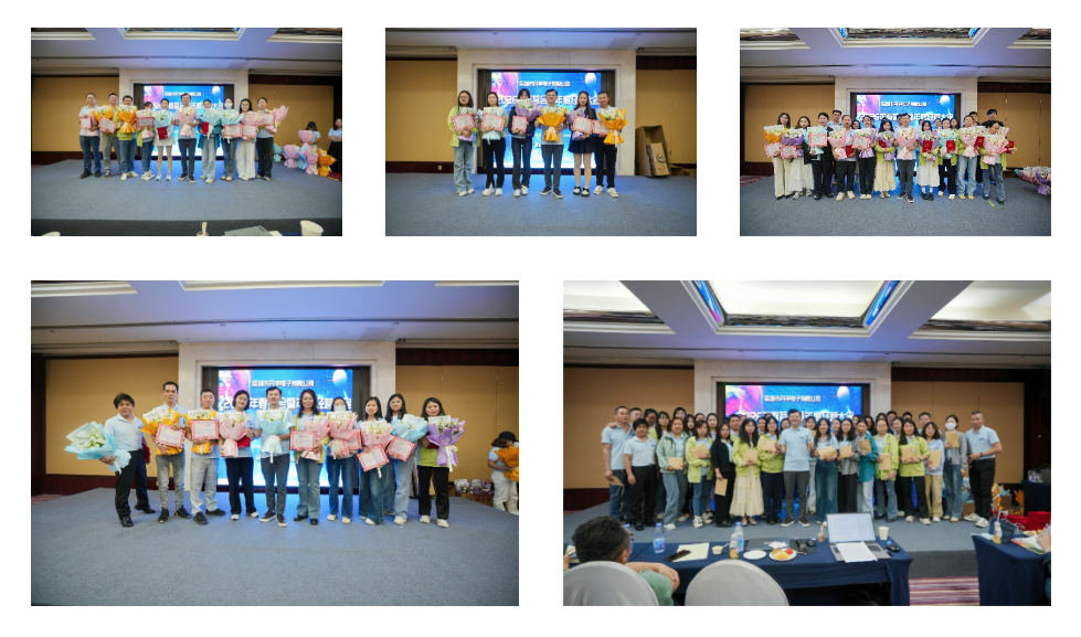
The event also included an employee recognition ceremony honoring team members for their long-term dedication and contribution. Based on years of service, EBest Circuit presented four honorary awards: the Leaf Award, Evergreen Award, Cultivation Award, and Dedication Award.
Each award represented more than years spent with the company. It recognized the consistency, responsibility, and effort that employees bring to their work every day. By celebrating these contributions, EBest Circuit reaffirmed its belief that long-term growth is built by people who grow together with the business.
A Strong Start to 2026
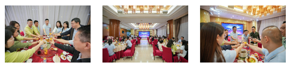
The event concluded with a team dinner, where employees gathered in a warm and relaxed setting to celebrate, connect, and look ahead together.
The 2026 Spring Banquet marked both a review of the past year and a meaningful start to the new one. By reflecting on achievements, addressing challenges, and aligning around shared goals, EBest Circuit further strengthened team cohesion and confidence for the future.
EBest Circuit sincerely thanks all employees for their dedication and continued commitment. The company also extends its gratitude to customers and partners for their trust and support. In 2026, EBest Circuit looks forward to creating greater value together and building an even stronger future with its team, customers, and partners.
About Us
Founded on June 28, 2006, EBest Circuit (Best Technology) is a trusted PCB and PCBA manufacturer focused on delivering one-stop PCB solutions to customers worldwide. With over 20 years of industry experience, we support customers from prototype to production with reliable manufacturing, engineering support, and responsive service.
Our product range covers: • Standard FR4 PCBs • Multilayer PCBs • Metal Core PCBs • Ceramic PCBs • Flexible and rigid-flex PCBs • RF and high-frequency PCBs • HDI PCBs • Heavy copper PCBs • Extra-thin PCBs • Busbar PCBs • High-speed and impedance control PCBs
Here are why customers work with EBest Circuit: • Over 20 years of PCB and PCBA experience • One-stop manufacturing service • Monthly capacity of 260,000 sq ft (28,900 m²) • More than 1,000 board types completed • Quick-turn service with urgent boards shipped within 24 hours • Continuous investment in R&D and product quality • Personalized customer support and long-term partnership focus
Our quality system is backed by certifications including: • IATF 16949 • ISO 9001:2015 • ISO 13485:2016 • AS9100D • REACH • RoHS • UL
Looking for a reliable PCB and PCBA manufacturing partner? Contact EBest Circuit today to discuss your project and discover how we can support your next product from prototype to mass production.
To learn more about EBest Circuit’s PCB and PCBA capabilities, please contact our team today for project support and manufacturing solutions.
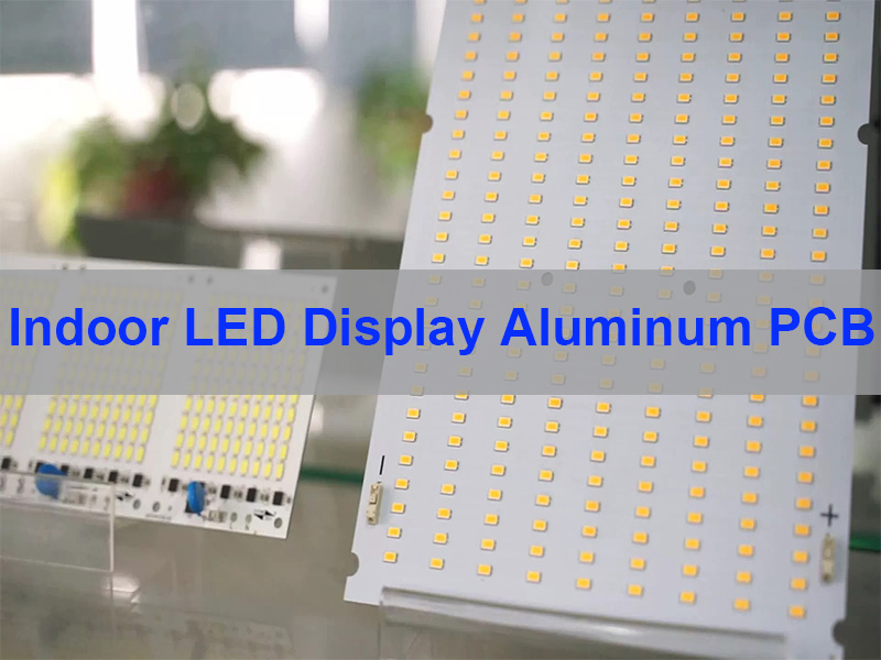
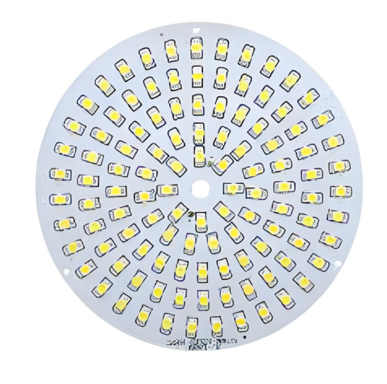
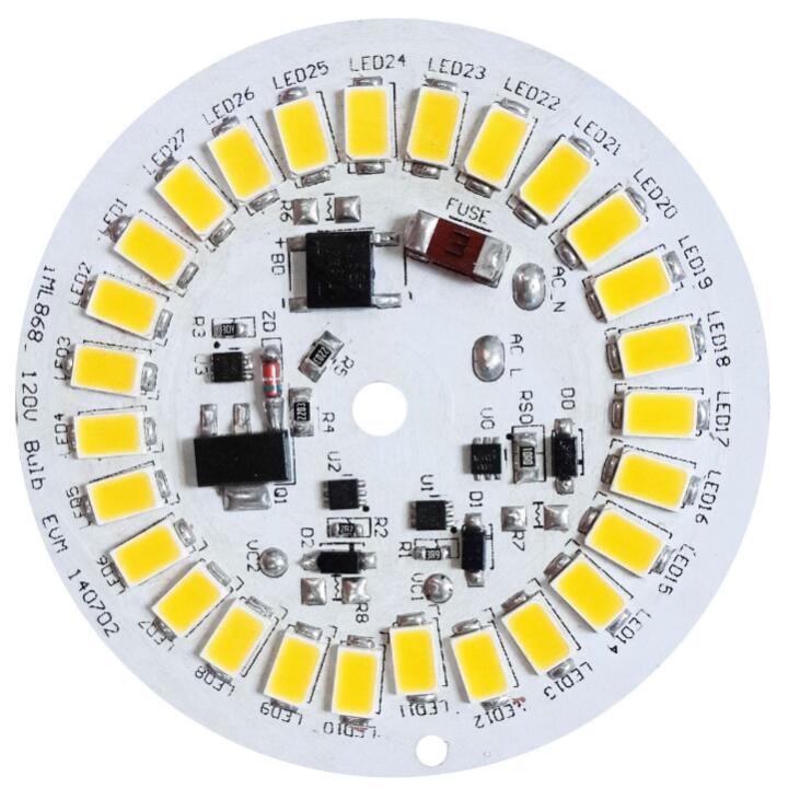
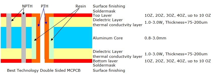
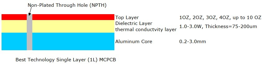
Indoor LED Display Aluminum PCB is a metal-core printed circuit board designed for indoor LED display modules, using an aluminum base to improve heat dissipation, enhance structural stability, and support reliable long-term display performance.
At EBest Circuit (Best Technology), we provide Indoor LED Display Aluminum PCB manufacturing with engineering support, fast response, and production control for stable indoor LED applications. We support customers who need dependable heat spreading, solid soldering performance, and repeatable quality for batch orders.
Core parameters customers often ask for
Base material aluminum core / metal core structure
Copper thickness 1oz, 2oz, or project-based design
Board thickness custom according to module structure
Thermal dielectric selected for indoor LED heat transfer needs
Surface finish HASL, ENIG, OSP, or project requirement
Quality controlled fabrication and assembly process for stable display modules
Lead time responsive support from sampling to volume builds
Service engineering communication that focuses on manufacturability and project fit
Supply continuity one-stop coordination for PCB fabrication and related assembly support
Therefore, a well-built aluminum PCB is not just a substrate choice, but the thermal foundation of indoor LED display reliability. In practice, buyers who start from board structure usually reduce downstream instability in the full module build.
What Is an Indoor LED Display Aluminum PCB and How Does It Work?
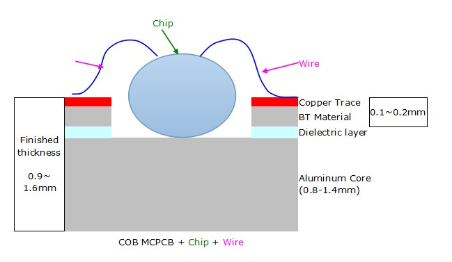
An Indoor LED Display Aluminum PCB is a metal-core circuit board designed to carry LED packages and related circuitry while moving heat away from the light source more efficiently than a standard FR4 board. It typically includes a copper circuit layer, a thermally conductive dielectric layer, and an aluminum base that spreads heat across a wider area.
For indoor LED displays, this structure matters because dense LED layouts can create local heat concentration. When heat is guided away quickly, the display is more likely to keep stable brightness, cleaner color performance, and longer service life.
Basic structure
Layer
Function
Why It Matters for Indoor LED Displays
Copper Circuit Layer
Carries current and signal paths
Supports LED connection stability and layout accuracy
Thermal Dielectric Layer
Transfers heat while keeping electrical insulation
Helps control heat flow from LEDs to the base
Aluminum Base
Spreads and releases heat
Improves thermal balance and mechanical support
Overall, this board type is chosen when thermal control and dimensional stability matter as much as electrical connectivity. This means it is especially suitable for indoor LED modules expected to run for long periods in conference and presentation environments.
Why Is Aluminum Better Than Standard FR4 for Indoor LED Display Thermal Control?
For many indoor LED display projects, aluminum offers a more practical thermal path than standard FR4 because it spreads heat faster and supports better mechanical rigidity. This is especially valuable in fine-pitch or high-density indoor displays where localized heating can affect both image quality and solder joint life.
FR4 still works in many electronics, but indoor LED display modules often benefit from the metal-core approach when brightness stability and long operating time are priorities. Aluminum also helps support flatter panel construction, which is useful when multiple modules must align into one seamless display surface.
Aluminum PCB vs FR4 for indoor LED display use
Item
Aluminum PCB for Indoor LED Display
Standard FR4 PCB
Heat spreading
Strong
Moderate
Suitability for dense LED arrays
High
Lower in thermal-heavy designs
Board rigidity
Better mechanical support
General-purpose support
Risk of thermal accumulation
Reduced with correct stack-up
Higher in high-density LED zones
Fit for quiet indoor display design
Very suitable
More limited in passive thermal design
As a result, aluminum is often the safer choice when the display must stay visually stable without relying heavily on extra cooling methods. From an engineering perspective, that makes the board itself part of the thermal solution rather than just a wiring platform.
How Does an Aluminum PCB Improve Meeting Room LED Display Performance?
In meeting rooms, the display is viewed at close distance, often for long sessions, so thermal consistency directly affects visual experience. A better thermal base helps the screen keep uniform brightness, cleaner white balance, and lower risk of color variation across modules.
It also supports quieter system design. Many indoor meeting room displays prefer passive or low-noise thermal strategies, and a well-designed Aluminum PCB for Indoor LED Display helps make that possible.
Performance gains that matter in meeting rooms
More stable brightness during long presentations
Lower thermal stress on LED packages and solder joints
Better module flatness for close-view visual consistency
Reduced chance of hotspots in dense pixel layouts
Improved fit for quiet indoor environments
In real-world applications, meeting room screens are judged by visual comfort as much as technical output. Notably, thermal control at the PCB level helps support both at the same time.
What Pain Points Do Buyers Face with Indoor Aluminum PCB LED Display Projects?
Buyers usually do not struggle with naming the product. They struggle with whether the board will stay stable after assembly, run cool enough in dense layouts, and remain consistent across batches. The most repeated concerns are warpage, poor heat flow, solder fatigue, uneven brightness, and production inconsistency from one build lot to another.
These issues often appear when the substrate choice, dielectric performance, copper design, and assembly process are not aligned from the start. That is why many indoor LED projects fail quietly during long operation, not during first power-on testing.
Common pain points and how we address them
Pain Point
What It Causes
How EBest Circuit Helps
Heat buildup in dense LED areas
Brightness drift and shorter life
Thermal-focused stack-up and process review
Board warpage or flatness variation
Poor module alignment and visual inconsistency
Controlled fabrication and dimensional inspection
Solder joint stress
Intermittent failures over time
Process control for stable assembly compatibility
Batch-to-batch inconsistency
Mixed display performance across modules
Standardized production control and traceable workflow
Unclear technical support
Design delays and manufacturability issues
Engineering communication before mass build
In short, the biggest risk is not one dramatic defect, but many small inconsistencies adding up in the finished display wall. To sum up, choosing a supplier that understands both PCB fabrication and LED display application logic helps prevent that chain reaction.
How Should PCB Aluminum for Indoor LED Display Be Designed for Better Heat Dissipation?
The answer is to treat thermal design as a full-board system, not a single material choice. A strong PCB Aluminum for Indoor LED Display design combines the right base thickness, proper dielectric selection, current path planning, copper balance, LED spacing, and interface design with the module frame or cabinet.
Many overheating problems come from poor heat path continuity. Even if the board uses aluminum, the result will be limited if copper distribution is uneven, thermal bottlenecks remain near LED clusters, or module contact to the supporting structure is weak.
Design focus areas
Keep heat-generating LEDs evenly distributed where possible
Use copper layout that supports both current carrying and heat spreading
Avoid sharp local thermal concentration under dense pixel zones
Match board flatness needs with module and frame requirements
Consider assembly process compatibility from the layout stage
Recommended design checkpoints
Checkpoint
Why It Matters
Dielectric thermal performance
Controls how effectively heat moves to the aluminum base
Copper balance
Supports thermal spreading and dimensional stability
LED package spacing
Reduces hotspot concentration
Panel flatness
Helps maintain seamless indoor display alignment
Assembly compatibility
Improves solder reliability and production repeatability
Meanwhile, the best thermal result usually comes from coordinated board and mechanical design rather than isolated PCB optimization. This means the aluminum substrate should be planned as part of the full display module architecture.
How Do We Manufacture LED Display Indoor Aluminum PCB for Stable Quality?
Stable manufacturing begins with material control and continues through imaging, etching, lamination, profile control, surface finishing, and final inspection. For LED Display Indoor Aluminum PCB products, process discipline is important because indoor LED modules require both thermal function and dimensional consistency.
Even small process variation can affect flatness, solderability, or thermal transfer behavior. That is why a production flow for LED display aluminum boards must focus on repeatability, not just output speed.
Typical manufacturing flow
Material confirmation based on thermal and structural requirement
Circuit pattern creation and copper processing
Dielectric and base structure control
Drilling, routing, and profile shaping
Surface finish selection for assembly compatibility
Electrical and dimensional inspection
Packing protection for safe shipment and module assembly readiness
What we pay special attention to
Dimensional stability across batches
Clean surface condition for reliable assembly
Flatness control for seamless module installation
Traceable production workflow for project consistency
From a manufacturing standpoint, indoor LED boards require consistency more than visual complexity. In practical terms, that consistency is what protects the final display from uneven module behavior after installation.
What Services and Certifications Should You Expect from an Indoor LED Aluminum PCB Supplier?
A capable supplier should provide more than bare board fabrication. You should expect technical communication, project review, documentation support, quality traceability, and clear manufacturing control for indoor LED applications. Certifications also matter because they indicate that the quality system is managed, repeatable, and suitable for customers who need dependable supply.
At EBest Circuit (Best Technology), we support LED-related PCB and PCBA projects with coordinated service from inquiry to delivery. For customers building Indoor Aluminum PCB LED Display products, this reduces handoff friction and helps keep engineering and production aligned.
Our service scope
Service Item
What It Supports
PCB fabrication
Aluminum and application-matched board manufacturing
Engineering review
Manufacturability and project feasibility check
Assembly support
Better connection between bare board and final product build
Project communication
Faster clarification of drawings and production needs
Traceable workflow
Improved batch control and follow-up support
Certificates
Certificate
What It Signals
ISO 9001
Managed quality system
ISO 13485
Controlled quality practices for medical-related manufacturing environments
IATF 16949
Automotive-oriented process discipline
AS9100D
Aerospace-oriented quality management capability
RoHS / REACH compliance support
Material and regulatory alignment for many global projects
Likewise, certifications alone do not guarantee a good project result, but they do show whether the supplier is operating with structured control. For buyers, that structure often translates into more predictable performance and smoother communication.
What Related Questions Do Buyers Commonly Ask Before Ordering Aluminum Indoor LED Display PCB?
Before placing an order, most buyers ask practical questions rather than abstract ones. They want to know which stack-up fits indoor fine-pitch modules, how flat the board can stay, whether the surface finish supports reliable assembly, and how to match the board to the module frame and display cabinet.
These questions are useful because they reveal the real success criteria of the project. A good supplier should answer them clearly before production starts.
High-interest questions often asked during inquiry
What board structure is best for indoor fine-pitch LED modules?
How do you control flatness for seamless indoor display assembly?
Which surface finish is better for LED module soldering?
How do you verify thermal performance in a dense LED layout?
Can the board design support long daily operating hours?
How do you maintain consistency across repeat production lots?
Besides, clear answers at the inquiry stage usually reduce revision loops later in the project. In engineering terms, early question quality often predicts final manufacturing smoothness.
How Does Display Indoor LED Aluminum PCB Support Long-Term Reliability?
Long-term reliability comes from controlling temperature, stress, and process variation together. A Display Indoor LED Aluminum PCB improves the first part by giving heat a faster path away from LEDs, but the full reliability result also depends on flatness control, soldering compatibility, and consistent material behavior over time.
When these factors work together, the display is more likely to maintain image uniformity and resist gradual degradation during long operation cycles. That matters in meeting rooms where the display must look stable every day, not only during initial testing.
Reliability factors linked to board design
Reliability Factor
Board-Level Impact
Heat control
Helps reduce LED aging speed
Mechanical stability
Supports better module alignment
Solder compatibility
Improves joint integrity over long use
Batch consistency
Keeps screen performance more uniform
Clean manufacturing
Reduces hidden process-related failure risk
By comparison, a board chosen only for basic connectivity may pass early testing but create hidden weakness later. Hence, reliability in indoor LED display projects should be designed into the substrate from the beginning.
What Are the Best Application Cases for Aluminum Indoor LED Display PCB?
The strongest application cases are indoor environments that demand close viewing, long operating time, and strong visual consistency. In these settings, Aluminum Indoor LED Display PCB products help support cleaner thermal performance and better screen stability than many standard board approaches.
Four industries stand out because they depend heavily on indoor display clarity and operating consistency. These examples also show why the board choice matters at the system level.
Typical industry cases
Industry
Typical Use
Why Aluminum PCB Helps
Corporate Meeting Rooms
Presentation walls and boardroom screens
Supports stable brightness and quiet thermal behavior
Control Rooms
Continuous-operation monitoring displays
Improves long-run thermal stability and screen consistency
Retail and Showrooms
Indoor branding and product presentation walls
Helps maintain visual uniformity during long opening hours
Education and Training Spaces
Lecture screens and collaborative display systems
Provides reliable operation for repeated daily use
Example use case
A fine-pitch indoor conference display with long daily operating time usually needs more than visual resolution. It also needs a board that supports uniform heat spreading across many closely packed LEDs, especially when the system is expected to remain quiet and visually consistent during extended meetings.
Ultimately, the best application is any indoor LED display where stable image quality matters over time. For that reason, aluminum PCB structures are often selected in projects that value both visual precision and operational confidence.
How Should You Choose the Right Supplier for LED Indoor Display Aluminum PCB?
You should choose a supplier that understands how PCB fabrication affects final display behavior. That means the supplier should be able to discuss thermal structure, flatness, copper design, assembly compatibility, process consistency, and project documentation with confidence.
A strong supplier is not only a factory. It is also a technical partner that can identify hidden manufacturability risks before they turn into module instability or field complaints.
What to evaluate during supplier selection
Experience with LED-related thermal board applications
Ability to communicate technical details clearly
Consistency in fabrication control and inspection
Support for repeat production with stable quality
Service response during design and order preparation
Quality system and certification visibility
Why many customers choose us
EBest Circuit (Best Technology) combines PCB manufacturing capability with application-focused support for demanding projects. For buyers of LED Indoor Display Aluminum PCB, that means smoother technical discussion, controlled production, and a stronger path from drawing to delivery.
Correspondingly, the right supplier helps reduce technical uncertainty before the first production lot begins. Overall, that is one of the most valuable advantages in indoor LED display manufacturing. If you are looking for a dependable supplier for Indoor LED Display Aluminum PCB, EBest Circuit (Best Technology) is ready to support your project. We provide professional Indoor LED Display Aluminum PCB products for indoor display applications. For inquiries and orders, pls feel free to contact us at sales@bestpcbs.com.
FAQs About Indoor LED Display Aluminum PCB
How does Indoor Aluminum PCB LED Display improve thermal performance?
It improves performance by transferring heat from the copper layer through a thermally conductive dielectric into the aluminum base, where heat can spread more efficiently. This helps reduce hotspot buildup and supports more stable long-term display operation.
Why use LED Display Indoor Aluminum PCB in meeting room screens?
Meeting room displays are viewed at short distance and often run for long sessions, so thermal stability directly affects image uniformity and reliability. Aluminum PCB structures help support quiet operation, stable brightness, and better module flatness.
How do you choose PCB Aluminum for Indoor LED Display?
Start by checking thermal requirements, LED density, board thickness, copper design, assembly compatibility, and flatness needs. The right choice is the one that matches both the electrical design and the mechanical structure of the display module.
What is the difference between FR4 and Indoor LED Aluminum PCB Display?
FR4 is a general-purpose substrate, while aluminum PCB includes a metal base that spreads heat more effectively. For indoor LED display modules with dense LED layouts, aluminum usually offers stronger thermal support and better dimensional stability.
How can EBest Circuit support Display LED Indoor Aluminum PCB projects?
We support customers with PCB fabrication, engineering communication, controlled production workflow, and quality-focused service for indoor LED applications. This helps reduce manufacturing risk and improves consistency from sample stage to repeat orders.
Can Aluminum Indoor LED Display PCB support long operating hours?
Yes, when the stack-up, dielectric, copper layout, and assembly conditions are designed properly, aluminum PCB structures are well suited for indoor displays that need stable thermal behavior during extended daily use.
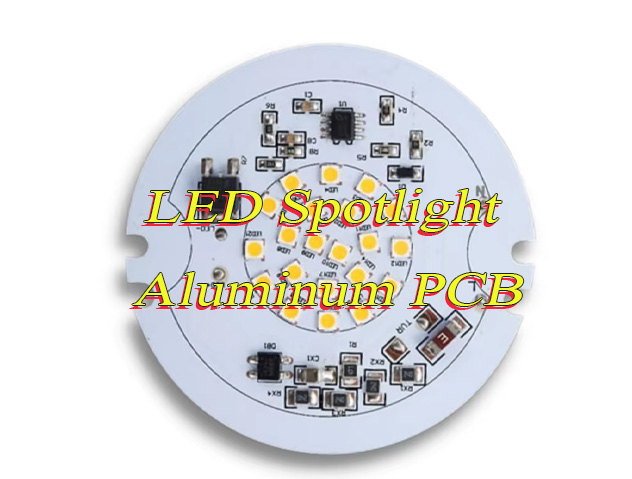
Are you struggling with heat buildup, blurred beam focus, or short lifespans in your LED spotlights that could be fixed with a high-performanceLED spotlight aluminum PCB? This guide breaks down everything you need to know about LED Spotlight Aluminum PCB, covering common industry challenges, targeted solutions, thermal performance fundamentals, and practical selection and testing tips for focused, reliable LED spotlight operation.
Common Challenges of LED Spotlight Aluminum PCB
Does insufficient thermal conductivity cause persistent heat buildup in LED spotlight aluminum PCB?
Can poor substrate bonding lead to layer separation and spotlight performance decline?
Does imprecise circuit layout disrupt beam alignment and cause light offset?
Can low-quality base aluminum reduce overall LED spotlight service life?
Does inconsistent thermal distribution create uneven brightness across the spotlight beam?
Our Solutions to the Above Challenges of Aluminum PCB for LED Spotlight
We engineer every LED spotlight aluminum PCB with multi-grade high thermal conductivity layers and optimized thermal via arrays, which quickly transfer concentrated heat from LED chips to the aluminum base and external heat sinks. This eliminates hotspots that damage chips and degrade performance, keeping junction temperatures within safe operating ranges for consistent lighting output.
We use industrial-grade, high-adhesion ceramic-filled dielectric materials paired with precision lamination technology under controlled temperature and pressure. This creates a permanent, stable bond between the copper circuit layer and aluminum base, preventing delamination even under long-term high-temperature continuous operation, and boosting overall structural durability.
Our team uses ultra-precision laser etching and computer-aided circuit layout design, with strict component placement tolerances and centered LED chip mounting. This locks in fixed beam alignment, eliminates light offset and uneven focus, and ensures the spotlight delivers sharp, consistent brightness as designed for commercial and architectural use.
We source 100% pure, high-grade aluminum base materials with consistent thermal conductivity and mechanical rigidity, rejecting low-purity alloys that warp or conduct heat poorly. This upgrade strengthens substrate durability, speeds up overall heat dissipation, and directly extends the continuous operational lifespan of the entire LED spotlight assembly.
We optimize full-surface thermal pathway design and uniform copper distribution across the LED spotlight aluminum PCB, ensuring even heat spread across all LED components. Balanced thermal control stops brightness fluctuations and flickering, delivering steady, flicker-free light output that meets quality standards for retail, hospitality and industrial spotlight applications.
Why Choose EBest as Your LED Spotlight Aluminum PCB Manufacturer?
EBest is a specialized, customer-focused LED spotlight aluminum PCB manufacturer with 20+ years of deep industry expertise, dedicated to solving the most pressing thermal and design pain points that cost lighting brands time, revenue, and customer trust. We don’t just build PCBs, we engineer solutions that directly boost your LED spotlight product quality, extend service life, and cut field failure rates, aligning every production decision with your bottom line and market competitiveness.
Our fully dedicated aluminum PCB production lines are equipped with precision automated equipment and run on 6-step strict quality control protocols, covering material inspection, lamination, etching, and finished product testing. Industry testing data confirms our LED Spotlight Aluminum PCB reduces LED chip junction temperature by up to 28°C compared to standard aluminum PCBs, and boosts spotlight service life by over 60% while cutting in-field failure rates by more than 75%.
Our in-house team consists of senior PCB engineers and LED lighting design specialists with an average of 15+ years of industry experience, offering free personalized technical support, custom circuit layout optimization, and free prototype testing for every client. We act as your long-term technical partner, not just a supplier, helping you refine spotlight performance from the initial design phase to mass production, and ensuring your final products stand out in the competitive commercial and industrial lighting markets.
We operate advanced, precision manufacturing facilities dedicated solely to aluminum PCB production, with strict quality control protocols at every production stage. Every LED Spotlight Aluminum PCB we make is built to meet or exceed global industry performance standards for thermal conductivity and structural stability.
Our team includes seasoned PCB and LED lighting engineers who provide free technical support, custom design adjustments, and prototype testing for clients. We don’t just supply PCBs – we partner with clients to optimize their LED spotlight performance from the design phase.
How Does High Thermal Conductivity Fix LED Spotlight Heat Buildup Issues?
High thermal conductivity in an LED spotlight aluminum PCB creates a direct, fast heat transfer path that pulls heat away from LED chips right as they generate it. Unlike standard PCBs that trap heat, this design stops heat from pooling and overheating sensitive LED components during daily operation.
This efficient heat flow lowers LED junction temperature by up to 28°C, a key metric that prevents performance fade and component damage. It also spreads heat evenly across the entire aluminum base, eliminating hotspots that cause early burnout and uneven brightness in spotlights.
By keeping operating temperatures stable, high thermal conductivity preserves consistent light output and extends the overall lifespan of LED spotlights. It also removes the need for bulky external heat sinks, making spotlight assembly simpler and more compact without losing cooling efficiency.
Why Do LED Spotlight Failures Tie Back to Poor Aluminum PCB Thermal Performance?
Most LED spotlight failures stem from unmanaged heat, and low-quality LED spotlight aluminum PCB is the root cause. LEDs convert 70-80% of energy into heat, and weak thermal conductivity traps this heat, pushing LED chip junction temps over the safe 85°C threshold quickly.
Consistent overheating degrades LED chip performance gradually, causing brightness fade, color shift, and full burnout over time. It also damages internal dielectric layers and circuit traces, leading to short circuits and sudden, unplanned spotlight failures.
Long-term heat stress warps thin or low-grade aluminum substrates, shifting optical lenses and LED chips to ruin beam alignment. This chain of damage drastically shortens spotlight lifespan and raises field failure rates, directly hurting product reliability.
What Thermal Conductivity Standards Work Best for Commercial LED Spotlights?
Commercial Spotlight Type
Recommended Thermal Conductivity (W/mK)
Applicable Industry Scenarios
Core Performance & Compliance
Low-Power Retail & Display Spotlights
1.0 – 2.0
Retail shelves, indoor display cabinets, hotel ambient lighting
IPC-6012 certified; steady low-heat dissipation, consistent soft brightness, no hotspots
Medium-Power Architectural Accent Spotlights
2.0 – 3.0
Building facades, gallery accent lighting, restaurant feature lighting
Balanced thermal control, stable beam alignment, resists thermal warping, long operational life
Rapid heavy heat dissipation, lowers LED junction temp by up to 28°C, cuts failure rates by 75%
How Does Aluminum PCB Design Impact LED Spotlight Beam Alignment & No Offset?
Beam alignment and zero light offset are critical for consistent, high-quality LED spotlight performance, and every detail of LED Spotlight Aluminum PCB design directly shapes these optical outcomes. Poor design choices cause unwanted beam shift, uneven light distribution, and off-center illumination, while precision-engineered PCB design locks in stable beam angle and eliminates offset for long-term reliable performance. Below are the key design factors that drive beam alignment.
Precision LED mounting pad positioning with tight ±0.05mm tolerance ensures accurate chip placement, matching the optical lens center perfectly to avoid initial beam offset.
Symmetric PCB substrate layout distributes weight and heat evenly, preventing one-sided warping that tilts LED chips and shifts the beam path.
Fixed, standardized lens holder mounting holes on the PCB maintain consistent lens-to-LED distance, avoiding height gaps that cause misaligned light projection.
Rigid substrate thickness (1.0–2.0mm for most spotlights) resists thermal warping under continuous operation, keeping optical components aligned without shifting.
Uniform copper trace layout avoids uneven heat concentration, preventing localized substrate bending that distorts beam direction over time.
Optimized LED array spacing and arrangement align with the designed beam angle, ensuring light overlaps evenly and eliminates off-center bright spots.
Flat, smooth substrate surface finish with zero bow or twist guarantees flush mounting of LED and optical parts, eliminating tilt-related beam offset.
Matched thermal expansion coefficient between aluminum base and dielectric layer prevents layer separation and substrate distortion during heating and cooling cycles.
Clear, accurate alignment markers on the PCB streamline assembly, reducing human error during component installation and ensuring consistent beam alignment across all units.
How to Test Aluminum PCB Thermal Efficiency for LED Spotlight Quality Control?
Thermal efficiency testing of LED Spotlight Aluminum PCB is a critical quality control step to verify heat dissipation performance, prevent LED overheating, and ensure long-term spotlight reliability. These tests cover lab-grade precision measurement, production-line quick screening, and long-term reliability validation, with clear, actionable methods for both small-batch sampling and mass production inspection.
Conduct infrared thermal imaging scanning under rated operating conditions to map surface temperature distribution and locate hotspots, ensuring no localized temperature exceeds the safe 85°C LED junction temperature threshold.
Perform thermal resistance testing per ASTM D5470 standard to measure heat transfer efficiency from LED mounting pads to the aluminum substrate base, a core metric for quantifying thermal conductivity performance.
Use laser flash analysis (ASTM E1461) to test bulk thermal conductivity of the aluminum base and dielectric layer, validating material consistency with stated specification values.
Run steady-state temperature testing: power the PCB with rated LED load, hold for 60 minutes until temperature stabilizes, and record temperature difference between LED chips and substrate surface.
Carry out transient thermal response testing to measure how quickly heat is pulled away from LED chips when powered on, confirming fast heat dissipation at startup.
Perform thermal cycling testing (-40°C to 125°C) to simulate extreme temperature changes, checking for thermal performance degradation or substrate warping after repeated cycles.
Conduct 168-hour continuous aging test at rated current to monitor temperature stability and ensure no gradual rise in operating temperature over extended use.
Test thermal consistency across production batches to confirm uniform heat dissipation performance, avoiding performance gaps between different PCB units.
Verify heat dissipation under simulated real-world conditions (with matching heat sink and enclosure) to replicate actual spotlight usage and validate practical thermal efficiency.
How to Balance Cost & Performance When Sourcing LED Spotlight Aluminum PCBs?
Balancing cost and performance when sourcing LED Spotlight Aluminum PCB means avoiding overpaying for unused specs while refusing low-grade materials that cause product failures and lost revenue. It focuses on smart specification matching, reliable supplier selection, and long-term value over short-term upfront savings, directly protecting your production efficiency and end-product quality.
Match thermal conductivity and substrate thickness precisely to your LED spotlight’s power rating and application, eliminating over-specified, high-cost features that deliver no real performance gain.
Prioritize suppliers with consistent batch quality and strict QC processes, like EBest, to reduce defective PCB rates and avoid costly production downtime and rework.
Choose standard aluminum alloy grades (5052/6061) for mainstream spotlights instead of rare, high-cost alloys, as these standard grades meet industry performance needs at a lower cost.
Optimize for moderate dielectric layer specifications that meet thermal and insulation requirements, avoiding premium ultra-thin dielectric layers unless needed for high-power models.
Order prototype PCBs for performance testing before full bulk orders, verifying thermal stability and optical compatibility to prevent mass production losses from mismatched parts.
Negotiate bulk pricing with a long-term reliable supplier instead of switching to low-cost unvetted suppliers, ensuring stable supply and consistent quality without hidden quality risks.
Avoid excessive customization on standard spotlight models; limit custom circuit layout and hole design only to specialized, high-value spotlight products.
Evaluate total lifecycle value instead of just upfront unit cost, as high-quality PCBs reduce field failures, maintenance, and replacement costs over the product’s lifespan.
FAQ About LED Spotlight Aluminum PCBs
Q1: What is the core difference between a standard PCB and an LED Spotlight Aluminum PCB? A1: A standard PCB is typically FR-4 fiberglass with thermal conductivity of just 0.2–0.3 W/mK, offering almost no heat dissipation, while an LED spotlight aluminum PCB has a 3-layer structure (copper circuit layer, thermally conductive dielectric layer, 5052/6061 aluminum base) with 1.0–5.0 W/mK thermal conductivity. This aluminum core design pulls heat away from LED chips 10–15x faster than standard PCBs, making it mandatory for heat-sensitive LED spotlight operation.
Q2: How does thermal conductivity affect LED spotlight lifespan and performance? A2: Higher thermal conductivity directly lowers LED junction temperature; every 10°C reduction in junction temperature doubles LED lifespan. For LED spotlights, a PCB with 3.0–5.0 W/mK thermal conductivity cuts junction temperature by up to 28°C compared to low-conductivity models, stopping light fade, color shift, and premature chip burnout, and extending total spotlight service life by 60% or more.
Q3: Can a custom LED Spotlight Aluminum PCB fix beam offset and focus issues? A3: Yes, a custom LED spotlight aluminum PCB eliminates beam offset and focus drift completely. Custom designs include ±0.05mm tolerance LED mounting pads, symmetric substrate layout, fixed lens holder holes, and 1.0–2.0mm rigid warp-resistant thickness, ensuring permanent alignment of LED chips and optical lenses, even under long-term thermal stress and continuous operation.
Q4: Are all aluminum substrates suitable for high-power LED spotlights? A4: No, only high-grade, thermally optimized 5052/6061 aluminum alloys with stable thermal conductivity and matched thermal expansion coefficients work for high-power (≥30W) LED spotlights. Low-grade recycled aluminum or non-specified alloys have uneven heat distribution, poor thermal stability, and high warpage risk, failing to dissipate heavy heat loads and causing rapid component failure.
Q5: How can I ensure the LED Spotlight Aluminum PCB I source meets quality standards? A5: Verify three key points: first, request ASTM D5470 thermal resistance test reports and IPC-6012 certification; second, order prototype samples for infrared thermal imaging and 168-hour aging testing; third, partner with a specialized manufacturer like EBest that provides full batch QC records and material certification, ensuring consistent performance and compliance with industry standards.
Order Your LED Spotlight Aluminum PCB from EBest Today
EBest specializes in high-performance LED Spotlight Aluminum PCB, designed to solve thermal, optical, and durability challenges for all LED spotlight applications. Whether you need standard or custom PCBs, we deliver reliable, high-quality products tailored to your needs.
Place your order or request a custom quote today by contacting us at sales@bestpcbs.com — our team is ready to support your LED lighting production needs with expert service and top-tier products.
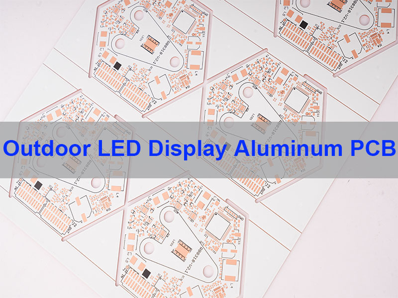
An Outdoor LED Display Aluminum PCB is used because it moves heat away faster, supports stable mounting, and helps the display hold brightness and color consistency over time. This article explains how to choose, design, and source the right Outdoor LED Display Aluminum PCB for waterproof applications. It covers board structure, thermal path design, waterproof strategy, reliability control, application examples, qualification points, and the service strengths of EBest Circuit (Best Technology).
EBest Circuit (Best Technology) is a professional manufacturer of Outdoor LED Display Aluminum PCB, with strong experience in waterproof, UV-resistant, and high-thermal aluminum PCB solutions for outdoor display applications. We help customers solve common issues such as short circuits, aging, uneven heat dissipation, black spots, and brightness decay under harsh outdoor conditions. Our team focuses on reliable thermal performance, structural fit, and stable quality, so customers can achieve more stable results in outdoor environments. We also support projects that need a good balance of reliability, qualification, and long-term supply stability. For Outdoor LED Display Aluminum PCB inquiries, please call +86-755-2909-1601.
Why Choose a Proven Outdoor LED Display Aluminum PCB Partner for Stable Waterproof Performance?
If you are sourcing Outdoor LED Display Aluminum PCB products, the right supplier should deliver more than bare fabrication. You need a partner that understands thermal structure, outdoor sealing, solder joint fatigue, uniformity control, and volume consistency.
EBest Circuit (Best Technology) supplies Outdoor LED Display Aluminum PCB solutions for demanding outdoor use. We support prototyping and production with engineering review, stack-up recommendation, DFM feedback, process alignment, and fast response for display projects that need both heat control and weather resistance.
Core parameters customers usually care about
Base material: aluminum metal core
Typical structure: copper circuit layer + dielectric + aluminum base
Typical board type: single-sided aluminum PCB, with selected hybrid structures when needed
Typical applications: billboards, transportation displays, stadium screens, building media walls
Why many buyers shortlist us
Quality: controlled fabrication and inspection flow for LED metal core boards
Lead time: responsive engineering support for urgent display programs
Service: technical communication that goes beyond simple quoting
Supply continuity: support for repeatable production and project follow-up
Therefore, the best supplier for this category is not just a board maker but a thermal and reliability partner. In practice, that directly affects brightness stability, installation life, and field maintenance frequency.
What Is an Outdoor LED Display Aluminum PCB and Why Is It Better for Waterproof Use?
An Outdoor LED Display Aluminum PCB is a metal-core circuit board built for LED systems that must run at higher current density and survive outdoor exposure. Its aluminum base spreads heat away from LEDs and driver-related hot zones much more effectively than standard glass-fiber boards in the same use case.
For outdoor display service, the board is only one part of the protection chain, but it is a critical one. It supports thermal control, mechanical rigidity, and better long-term dimensional stability in assemblies that operate in sun, rain, dust, and humidity.
Basic structure
Copper layer: carries current and LED interconnect routing
Dielectric layer: provides electrical insulation while passing heat downward
Aluminum base: spreads heat into the housing or thermal structure
Why this matters outdoors
Lower hotspot accumulation
Better support for high-brightness duty
Improved mechanical support for module installation
Better match for thermal management assemblies
As a result, Aluminum PCB for Outdoor LED Display projects usually deliver a more stable operating platform than ordinary FR4-only designs. From an engineering perspective, that stability is what turns a bright screen into a durable outdoor product.
Why Does Aluminum PCB Matter So Much in Outdoor LED Display Thermal Design?
The short answer is heat. Outdoor displays operate under sunlight, high ambient temperature, dense LED placement, and long daily runtime. If heat is not moved away quickly, brightness drops, color shifts increase, and solder joints age faster.
In many outdoor LED systems, thermal load is not just generated by the LEDs themselves. Driver devices, current distribution, enclosure heat buildup, and limited airflow can raise the entire module temperature. That is why the thermal path must be planned as a full system, not just as a board material choice.
Where the heat goes
LED junction generates heat
Heat passes through solder and copper pad
Heat crosses the dielectric layer
Aluminum base spreads heat laterally
Heat transfers into the module frame or heat-dissipation structure
What a good thermal design improves
Brightness retention
LED lifetime consistency
Solder joint reliability
Color uniformity across the panel
Reduced risk of local overheating
In real-world applications, thermal performance is the first reason buyers move from standard PCB concepts to Outdoor Aluminum PCB LED Display structures. Overall, better heat flow means better visual stability and lower field failure pressure.
How Is an Outdoor LED Display Aluminum PCB Built for Heat Transfer and Mechanical Strength?
The board is usually built as a layered thermal structure rather than a standard multilayer logic board. The goal is to keep electrical routing simple and the thermal route short, direct, and repeatable.
Most outdoor display aluminum boards use a copper circuit layer on top, a thermally conductive dielectric in the middle, and an aluminum base underneath. The exact dielectric choice matters because it must balance insulation and heat transfer while surviving assembly heat and outdoor service stress.
Typical design considerations
Copper thickness: chosen to handle current and voltage drop
Dielectric performance: important for thermal resistance and insulation reliability
Aluminum thickness: affects stiffness and heat spreading
Board flatness: important for LED placement and waterproof mechanical fit
Mechanical advantages
Higher rigidity than very thin conventional boards
Better support for module fastening
Reduced deformation risk during installation
Improved contact with metal housings or thermal interfaces
In short, a good LED Display Outdoor Aluminum PCB is both a circuit carrier and a thermal-mechanical platform. Notably, that dual role is one reason it remains the preferred base for high-output outdoor LED modules.
How Does Waterproof Design Work in PCB Aluminum for Outdoor LED Display?
A waterproof outdoor display is never achieved by the PCB alone. It comes from a complete sealing system that includes the board surface, LED package area, connectors, cable exits, gasket interfaces, screws, rear cover, and enclosure design.
The aluminum PCB still plays an important role because its rigidity and thermal behavior support a more stable assembly. However, rain resistance, dust protection, and moisture control depend on system-level integration.
Main waterproof design elements
Protective mask and controlled surface finish compatibility
Sealant-compatible module edges
Waterproof connectors and cable entry control
Rear cover sealing and vent planning
Conformal protection where the design requires it
Drain path planning to avoid trapped water
Design Area
What It Must Control
Why It Matters
PCB surface protection
Moisture, contamination, corrosion
Protects conductive features and solder joints
LED and component interface
Seal continuity and material compatibility
Prevents moisture ingress near active parts
Connector area
Water entry through wiring paths
Common field failure point
Cabinet interface
Rain splash, dust, temperature cycling
Defines long-term outdoor sealing stability
Drainage and venting
Condensation and trapped moisture
Reduces hidden water accumulation
This means, a robust PCB Aluminum for Outdoor LED Display design should be reviewed as a full outdoor module system. To sum up, the best waterproof result comes from sealing, drainage, coating, and thermal design working together.
What IP Level Is Common for Outdoor LED Aluminum PCB Display Systems?
For most outdoor screen modules, buyers usually expect front-side protection around IP65 or above, while rear-side protection depends on cabinet structure and installation conditions. The actual target should match the use environment, service method, and enclosure design.
In practical sourcing, it is a mistake to ask only whether the board is waterproof. The better question is whether the entire Outdoor LED Aluminum PCB Display module is engineered to meet its intended outdoor protection level in real installation conditions.
How to interpret the protection need
Front side: exposed to rain, dust, washing, and wind-driven water
Rear side: depends on enclosure type and site exposure
Connector area: often needs separate protection review
Maintenance style: front service and rear service affect sealing design
Outdoor Condition
Typical Protection Expectation
Design Priority
Urban billboard
High front-side weather resistance
Rain sealing and heat management
Building facade
Stable front protection with controlled rear area
Module sealing and cable entry control
Coastal installation
Higher corrosion resistance focus
Anti-moisture and anti-salt strategy
Harsh climate zone
Enhanced sealing and thermal margin
Condensation control and reliability reserve
From an engineering perspective, protection level should be defined by the installation scenario, not by marketing language alone. In practice, that is how a sourcing team avoids under-designed outdoor modules.
How Does Outdoor Heat, Rain, Dust, and Humidity Damage LED Display Boards?
Outdoor LED boards do not fail from one cause only. Real failures often come from combined stress such as heat plus humidity, rain plus poor sealing, or thermal cycling plus weak solder joints. That is why reliability planning must be multidisciplinary from the start.
Heat can reduce brightness stability and accelerate aging. Moisture can trigger corrosion, leakage, and intermittent faults. Dust reduces heat release efficiency. Salt and pollution make corrosion more aggressive in coastal or industrial environments.
Common field risks
Brightness drop under high temperature
Color inconsistency after long operation
Dead pixels caused by thermal fatigue or moisture damage
Corrosion on exposed conductive areas
Short circuit risk from water ingress or condensation
Mechanical stress from daily temperature swings
What reliable designs do differently
Build thermal margin into the board and housing
Protect vulnerable regions from moisture entry
Control contaminants during fabrication and assembly
Validate the module under realistic outdoor conditions
Overall, outdoor reliability depends on preventing compound failure modes rather than fixing one issue in isolation. Therefore, a serious Outdoor LED Display Aluminum PCB program should always include both thermal and environmental validation.
Why Do Buyers Often Ask About User Pain Points Before Ordering Outdoor LED Display Aluminum PCB?
Because the same problems appear again and again in outdoor LED projects. Buyers want to avoid screens that run too hot, fail after rain, show uneven brightness, or become difficult to maintain after installation. Those concerns are far more common than abstract material questions.
Across public discussions and application-focused content, the recurring pain points are clear: sealing confidence, real thermal performance, corrosion resistance, long-term uniformity, and the gap between quoted spec and field behavior.
Typical buyer pain points
Not sure whether the board can support high brightness continuously
Concern about rain, condensation, and seal aging
Worry about dead pixels and solder fatigue after thermal cycling
Need stable quality across repeat orders
Need engineering support instead of quote-only communication
Want simpler sourcing with a responsive manufacturer
How EBest Circuit (Best Technology) addresses them
Engineering-first review for thermal path and manufacturability
Clear communication on board structure and application fit
Process control for repeatable quality
Support for outdoor-use reliability expectations
Responsive service for prototype and production stages
Notably, buyers usually stay with suppliers who reduce technical uncertainty early. As a result, choosing a supplier that understands real field pain points can shorten development cycles and improve launch confidence.
What Services and Certifications Should You Expect from an Outdoor LED Display Aluminum PCB Supplier?
A credible supplier should offer more than fabrication capacity. For this product category, you should expect engineering support, manufacturability review, stable process execution, inspection discipline, and documented quality systems.
EBest Circuit (Best Technology) supports customers with LED PCB manufacturing and technical communication for outdoor applications. Buyers also look for certificate visibility because it shows the factory operates with formalized systems rather than informal process control.
Service scope you should expect
Engineering review for structure and manufacturability
Prototype support for fast verification
Production support for volume continuity
Inspection control for board consistency
Technical communication through project follow-up
Category
What It Shows
Why It Helps Buyers
Quality management certification
Controlled documented processes
Improves confidence in repeat production
Environmental compliance support
Material and process conformity awareness
Helps global sourcing coordination
Manufacturing process discipline
Inspection and control checkpoints
Reduces variation risk
Engineering support capability
Problem-solving before production
Improves project efficiency
In real-world sourcing, certifications do not replace engineering capability, but they do strengthen trust. In short, the best supplier combines documented quality systems with practical LED thermal know-how.
What Design Rules Improve Manufacturability for Aluminum PCB for Outdoor LED Display?
A board can look good in layout software and still perform poorly in manufacturing or field service. Good manufacturability means the design is easy to fabricate, easy to assemble, thermally balanced, and stable during long-term use.
For Aluminum PCB for Outdoor LED Display products, manufacturability is especially important because LED arrays expose every inconsistency. Uneven pad design, copper imbalance, poor spacing decisions, and weak mechanical planning can all show up later as visible display defects.
Important design priorities
Keep thermal paths short and direct
Use balanced pad and copper planning for uniform heat spread
Maintain good spacing for assembly quality and contamination control
Consider flatness and module mounting from the start
Match connectors and sealing features to service conditions
Review current carrying capacity, not just routing completion
Typical DFM review points
Review Point
Why It Matters
Impact on Outdoor Use
Pad design consistency
Improves solder quality
Reduces uneven optical performance
Copper distribution
Supports heat spread and flatness
Improves stability under thermal load
Mounting hole strategy
Protects board integrity
Helps cabinet integration
Surface protection compatibility
Supports coating and sealing
Improves weather durability
This means, manufacturability is not separate from reliability in outdoor LED boards. From an engineering perspective, good DFM choices reduce both process risk and field repair pressure.
How Does Outdoor LED Display Aluminum PCB Compare with FR4 for High-Brightness Screens?
For low-power electronics, FR4 is a proven standard material. For outdoor high-brightness LED display boards, aluminum-based structures are often the better fit because they handle heat spreading and mechanical support more effectively.
The decision is not about one material being universally better. It is about matching the substrate to the thermal load, brightness target, operating environment, and service expectations of the final product.
Item
Outdoor LED Display Aluminum PCB
FR4 PCB
Heat dissipation
Strong heat spreading through metal base
Much lower thermal conduction in standard form
Mechanical rigidity
Good structural support for LED modules
Depends on thickness and support design
Outdoor high-brightness suitability
Very suitable
Limited for thermally stressed designs
Thermal path simplicity
Direct and efficient
Often needs extra thermal measures
Typical use focus
LED lighting and display modules
General electronics and control circuits
Overall, aluminum becomes the practical choice when heat and outdoor duty cycle drive the design. Therefore, many high-output display projects move to Outdoor LED Display Aluminum PCB when they need stronger thermal margin.
How Is an Outdoor Aluminum PCB LED Display Project Manufactured Step by Step?
The manufacturing route must protect both electrical quality and thermal integrity. Unlike a generic board flow, an outdoor LED metal-core board needs tighter attention to dielectric handling, surface consistency, routing quality, and final flatness.
A stable process also helps later waterproof assembly because a well-controlled board fits more predictably into module housings, gaskets, and sealed mechanical structures.
Typical process flow
Engineering file review and manufacturability confirmation
Material preparation and metal-core laminate selection
Circuit imaging and etching
Drilling, routing, and profile control
Solder mask and surface finish processing
Dimensional, appearance, and electrical inspection
Packing and shipment control for board protection
What the factory must watch closely
Dielectric integrity
Trace and pad precision
Board flatness
Surface cleanliness
Edge quality for later sealing and assembly
As a result, production quality on this board type is tightly linked to final display reliability. Notably, buyers who review process discipline early usually avoid many later installation issues.
What Four Industries Commonly Use LED Display Outdoor Aluminum PCB Solutions?
The most active sectors are those that need high brightness, reliable outdoor visibility, and long operating hours. In these applications, the board must support stable light output while tolerating weather and installation stress.
1. Outdoor advertising and media
Large billboards and building screens need stable brightness, color consistency, and low maintenance pressure. The LED Display Outdoor Aluminum PCB helps manage thermal load in dense, high-visibility installations.
2. Transportation and traffic information
Roadside information boards, station displays, and public guidance systems need dependable operation in changing weather. Good thermal design and sealing reduce service interruptions.
3. Stadium and event screens
These projects face strong daylight, long runtime, and visibility demands. Board stability matters because hot spots and module inconsistency quickly become visible on large display surfaces.
4. Retail facade and commercial exterior signage
Exterior brand displays need slim structures, stable brightness, and attractive long-term appearance. Aluminum PCB solutions help balance compact design with thermal control.
Industry
Main Need
Why Aluminum PCB Helps
Advertising
Long runtime and brightness stability
Better heat handling for continuous operation
Transportation
Outdoor reliability
Supports stable thermal and mechanical performance
Stadiums
High visual consistency
Reduces thermal unevenness across modules
Retail exteriors
Compact structure and weather resistance
Improves heat spread in limited space
In practice, these industries choose aluminum boards because visibility and uptime are directly linked to revenue or public function. To sum up, the board is not just a material choice but a performance enabler for outdoor display systems.
How Should You Evaluate a Supplier Before Ordering Outdoor LED Display Aluminum PCB?
Before placing an order, look at engineering fit, process stability, communication quality, and repeatability. A visually attractive quote means little if the supplier cannot explain thermal structure, protection strategy, and application compatibility.
Useful evaluation questions
Do they understand outdoor display thermal paths?
Can they discuss dielectric and aluminum structure clearly?
Do they review manufacturability before production?
Can they support repeat orders with stable quality?
Do they communicate clearly on lead time and project status?
Can they align the board with your module and enclosure strategy?
Green flags in supplier communication
They ask about brightness, environment, and service conditions
They review drawings instead of quoting blindly
They discuss reliability, not only board thickness
They show an organized approach to quality documentation
This means, a good supplier reduces project risk before production begins. Overall, the best sourcing decision comes from technical clarity, not from generic product language.
Why Choose EBest Circuit (Best Technology) for Outdoor LED Display Aluminum PCB Orders?
If your project needs a reliable Outdoor LED Display Aluminum PCB, EBest Circuit (Best Technology) can support you with practical engineering communication and production-oriented service. We understand that outdoor LED boards must balance heat transfer, structural fit, manufacturability, and long-term use stability.
We work with customers who need more than a standard board quote. Our goal is to help you move from concept to repeatable production with clearer technical decisions, better fit for outdoor applications, and smoother project follow-up.
What we offer for this product type
Outdoor LED aluminum PCB support for display-related applications
Engineering review before production
Responsive communication during project execution
Prototype to production support for ongoing programs
Quality-focused process control for stable repeat orders
If you are looking for a dependable source for Aluminum PCB for Outdoor LED Display products, EBest Circuit (Best Technology) is ready to support your order. Please send your project files and inquiry to sales@bestpcbs.com.
Therefore, choosing the right partner helps you improve both product confidence and sourcing efficiency. In real-world applications, that can make a visible difference in launch speed and long-term display stability.
FAQs About Outdoor LED Display Aluminum PCB
Why is Outdoor Aluminum PCB LED Display better than standard FR4 in high-brightness use?
Because outdoor screens usually run hotter and longer. Aluminum-based boards spread heat more effectively, which makes them better suited to high-output LED modules exposed to sunlight and changing ambient temperature.
What industries most often use Outdoor LED Aluminum PCB Display products?
The most common industries are outdoor advertising, transportation displays, stadium screens, and exterior commercial signage. These sectors need stable brightness, weather resistance, and long operating life.
How do aluminum PCBs protect outdoor LED signs from extreme weather?
Beyond heat dissipation, aluminum provides high dimensional stability and mechanical durability. Outdoor displays face extreme temperature fluctuations (from freezing nights to scorching days) which can cause standard boards to warp or crack. Aluminum has a lower coefficient of thermal expansion than FR4, meaning the board maintains its shape better. Additionally, most outdoor aluminum PCBs receive specialized surface treatments like anodizing or polyurethane coating to provide a robust barrier against moisture, salt spray, and UV-induced corrosion.
What are the design limitations of using aluminum PCBs for LED modules?
The main trade-off for the thermal benefits of aluminum is limited circuit complexity. Because the base is a conductive metal, aluminum PCBs are typically restricted to single-layer or simple double-layer designs. Creating multilayer stacks is significantly more expensive and technically difficult compared to FR4. Designers must also account for:
Rigidity: Aluminum cannot be used for curved or flexible display designs.
Component Mounting: Only Surface Mount Technology (SMT) is practical; Through-Hole Technology (THT) is generally not possible because the metal base would short the component leads.
Why order Outdoor LED Display Aluminum PCB from EBest Circuit (Best Technology)?
Because we provide product support with practical engineering communication, quality-focused manufacturing control, and responsive service for outdoor LED projects. If you need Outdoor LED Display Aluminum PCB products, contact sales@bestpcbs.com to discuss your order.
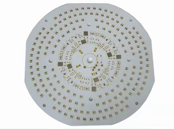
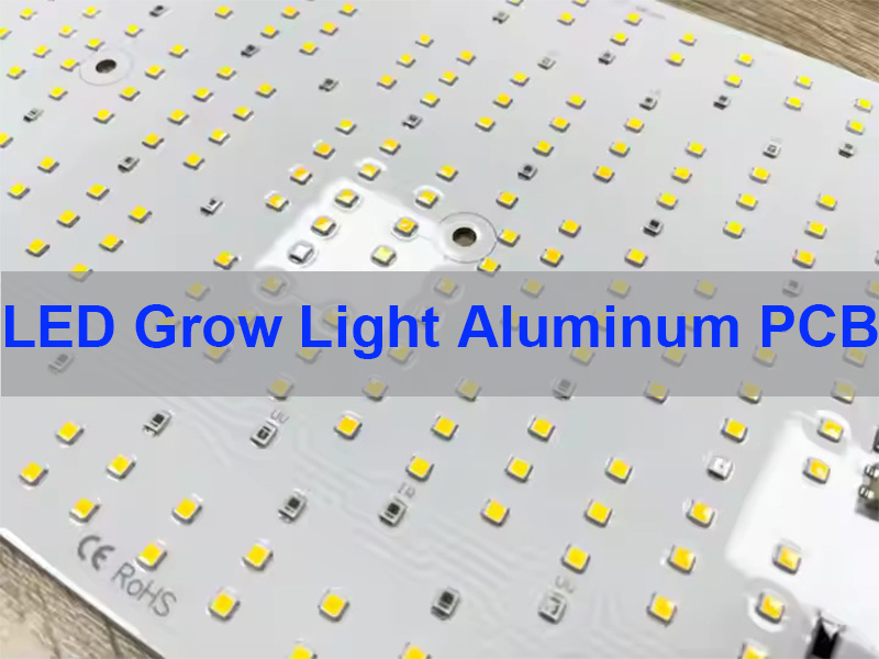
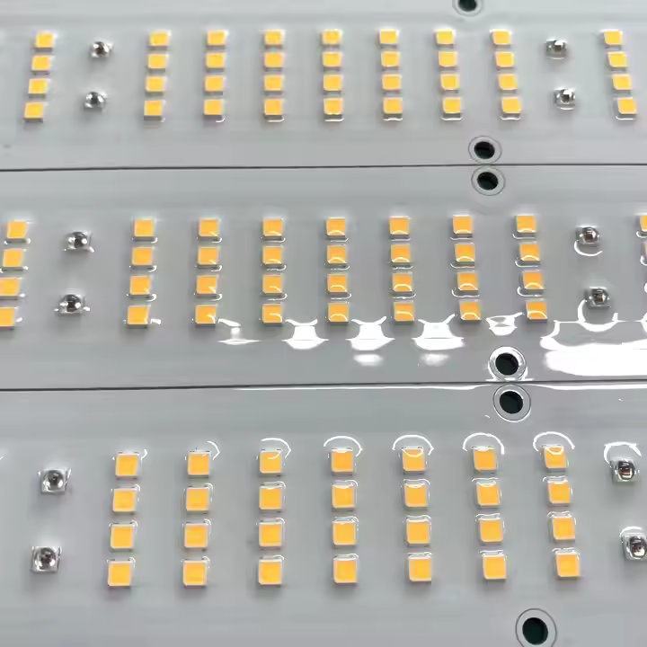
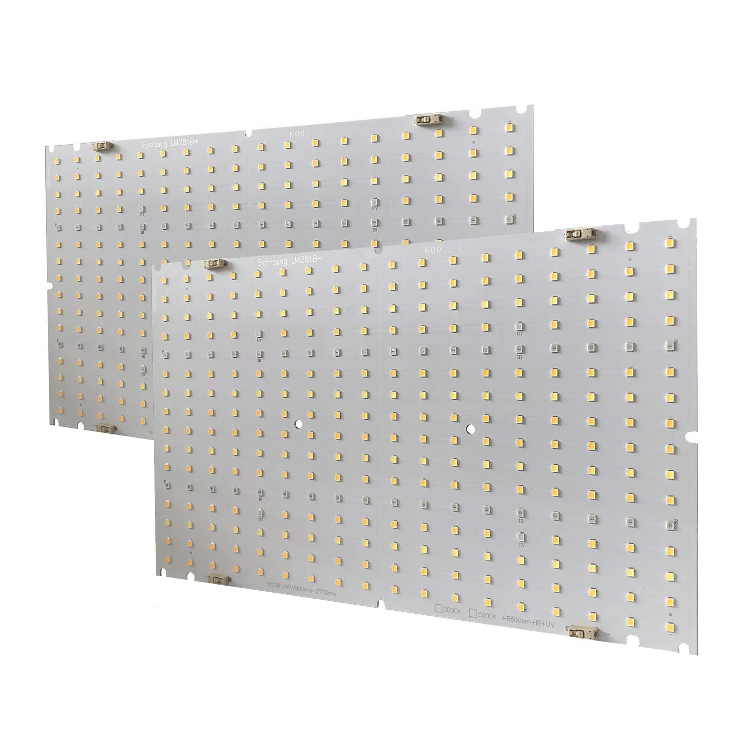
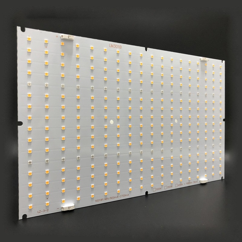
LED Grow Light Aluminum PCB is a metal-core printed circuit board designed for grow lighting systems, using an aluminum base to improve heat dissipation, support high-density LED layout, and ensure stable long-term lighting performance. This article explains how LED Grow Light Aluminum PCB designs work, what parameters matter before production, how to improve thermal reliability, and how to choose the right manufacturing partner for custom projects.
EBest Circuit (Best Technology) is a professional LED Grow Light Aluminum PCB manufacturer with solid experience in thermal design, spectrum-compatible PCB structure, and stable production for plant lighting applications. We understand that grow light projects are not only about making a board, but about balancing heat dissipation, spectrum layout compatibility, structural reliability, and long-term operating stability in real working conditions. For customers who care about thermal consistency, optical adaptation, scalable supply, and dependable long-run performance, we provide practical engineering support from PCB design review to manufacturing execution. Whether your focus is product quality, thermal efficiency, structural matching, or batch supply capability, our team can help turn your grow light concept into a production-ready and reliable solution. Pls feel free to contact us anytime at +86-755-2909-1601 to discuss your LED Grow Light Aluminum PCB project.
What Is LED Grow Light Aluminum PCB and Why Is It Common in Plant Lighting?
LED Grow Light Aluminum PCB is a metal-core circuit board built with an aluminum base to improve heat dissipation for LED lighting applications. In plant lighting, it is commonly used because the board must support continuous operation, high LED density, and stable junction temperature under demanding daily use.
Compared with a standard board, an aluminum-based structure moves heat away from the LED package more efficiently. That helps reduce thermal accumulation and supports more consistent optical and electrical performance across the board.
Why it is widely used in grow lights
Supports high-power and medium-power LED arrays
Improves thermal spreading across long bars and panel boards
Provides good mechanical support for thin or extended fixtures
Works well in linear, strip, round, and custom fixture designs
For many horticulture products, the board is not just a substrate. It is a thermal platform. That is why board selection has a direct effect on performance and service life.
Notably, aluminum PCB is common in grow lights because thermal control and structural stability matter every day of operation. To sum up, it offers a practical foundation for reliable LED plant-lighting assemblies.
Why Is Aluminum PCB Better Than Standard FR4 for Grow Light Applications?
For most grow-light boards, aluminum is preferred because the job is thermal before it is decorative. Standard FR4 can still work in lower-power designs, but once LED density rises, heat becomes harder to spread and remove. That is where aluminum PCB offers a clear advantage.
Aluminum PCB versus FR4 for grow light products
Item
Aluminum PCB
FR4 PCB
Heat dissipation
Strong
Moderate
Rigidity
Higher
Moderate
LED density fit
Better
Limited
Heatsink coupling
Direct
Indirect
Typical use
Light engine
Control board
Long-run stability
Better
Lower
This does not mean FR4 has no place. In many fixtures, the driver or control section can still use FR4, while the LED light board uses aluminum. That mixed approach is practical when each board has a different job.
As a result, aluminum PCB is usually the better fit when the LED board carries the real thermal load. From a product standpoint, that helps keep the fixture more stable during sustained use.
How Is an Aluminum PCB LED Grow Light Board Structured?
The structure of an Aluminum PCB LED Grow Light board is simple in appearance but important in function. A typical board contains a copper circuit layer, a thermally conductive dielectric layer, and an aluminum base. These layers work together to carry current, insulate electrically, and move heat downward into the metal substrate.
Main layers in a typical grow light aluminum PCB
Copper circuit layer for electrical routing and LED pad connection
Thermal dielectric layer for electrical isolation with heat transfer capability
Aluminum base layer for heat spreading and structural support
Optional design elements
Solder mask and legend
Reflective white surface for light efficiency in some designs
Mounting holes for direct heatsink fastening
Connector areas for modular assembly
Custom outline for bars, rings, panels, or segmented boards
Good structure selection is not only about thermal conductivity. It is also about assembly compatibility, flatness, and whether the board fits the mechanical design of the final lamp.
In real-world applications, the board stack directly shapes thermal behavior and assembly stability. Therefore, the structure should always be chosen with the final fixture in mind.
Why More Buyers Start with the Right LED Grow Light Aluminum PCB Partner?
If your end product depends on stable brightness, even heat spreading, and repeatable assembly, your supplier choice affects the result from the first file review. A capable manufacturer does more than make a board. They check thermal paths, pad geometry, current load, soldering windows, and the match between board design and final fixture structure.
That matters even more in plant lighting. These products often run for long daily cycles, use dense LED arrays, and work in warm or humid environments. A weak board design can lead to hot spots, color shift, shortened LED life, or uneven performance across the fixture.
What you should expect before placing an order
Core parameter review including board size, aluminum thickness, copper weight, thermal dielectric, voltage, current, LED count, and mounting method
DFM support to improve manufacturability before tooling starts
Assembly compatibility checks for SMT process, reflow profile, connector fit, and final heatsink attachment
Project communication that is fast, clear, and technical enough to solve issues early
If you are sourcing PCB Aluminum LED Grow Light products for a new or ongoing project, EBest Circuit (Best Technology) can support fabrication, assembly, and engineering review in one workflow. Send your files to sales@bestpcbs.com for a technical evaluation and production support.
Therefore, a strong supplier reduces redesign risk before the first batch starts. In practice, that improves manufacturability, thermal stability, and delivery confidence at the same time.
Why Choose Us for LED Grow Light Aluminum PCB?
Buyers do not only compare boards. They compare consistency, response speed, process control, and whether a supplier can support real production conditions. For LED Grow Light Aluminum PCB projects, the most important value usually comes from thermal design awareness, assembly experience, and supply continuity.
Quality focus with controlled manufacturing and inspection for aluminum PCB and LED assembly projects
Lead time support for samples, pilot runs, and repeat production
Engineering service with DFM feedback, stack-up advice, and assembly-oriented review
Supply support for PCB fabrication, SMT assembly, and one-stop project coordination
Communication efficiency so technical questions are solved quickly instead of being delayed between teams
What this means for your project
A grow light board is not just a lighting PCB. It is part of a full thermal and electrical system. We review the board as a working product, not as an isolated drawing. That helps reduce board warpage risk, poor solder joints, current imbalance, and avoidable layout revisions.
For buyers looking for Light Grow LED Aluminum PCB, Grow Light Aluminum PCB LED, or PCB LED Grow Light Aluminum production support, we can help turn design data into a stable and repeatable build.
Overall, choosing the right manufacturer improves both board performance and project coordination. As a result, the product reaches assembly with fewer unknowns and better long-term consistency.
What Services and Certifications Should a LED Grow Light Aluminum PCB Supplier Have?
A qualified supplier should offer more than bare-board fabrication. For horticulture lighting, it is better to work with a manufacturer that can review the design, build the board, assemble the LEDs, and control traceability during production. That shortens communication loops and helps keep thermal and assembly decisions aligned.
Our service scope and certifications
Category
Details
Why It Matters for LED Grow Light Aluminum PCB
PCB Fabrication
Aluminum PCB, MCPCB, custom board sizes, prototype to production
Supports custom thermal structures and LED board formats
PCBA Service
LED SMT assembly, connector assembly, functional support
Improves build consistency for populated grow light boards
Engineering Support
DFM review, pad design check, manufacturability advice
Helps prevent rework and process instability
Supply Coordination
One-stop handling for PCB and assembly workflow
Reduces handoff issues between multiple vendors
ISO 9001
Quality management system
Supports process discipline and documentation control
ISO 13485
Medical quality system capability
Shows strong process rigor and traceability awareness
IATF 16949
Automotive quality system capability
Reflects high expectations for consistency and process control
AS9100D
Aerospace quality system capability
Demonstrates disciplined production management
These capabilities are useful because many grow-light projects move from custom sampling into recurring production. A supplier with stable systems is better prepared for that transition.
From an engineering perspective, service range and quality systems directly affect repeatability. In real-world projects, that means smoother transfer from design files to finished boards.
What Problems Do Buyers Usually Face with LED Grow Light Aluminum PCB Projects and How Do We Solve Them?
Most buyers are not struggling with the basic concept of an aluminum board. They struggle with execution. The common problems are uneven temperature rise, unstable assembly yield, unclear design input, LED mismatch, and uncertainty about how the board will behave once mounted into a real fixture.
Common pain points and our solutions
Pain Point
Typical Issue
Our Support
Thermal hot spots
Uneven heat
Thermal layout review
Unclear files
Missing notes
Early file check
Assembly instability
Solder inconsistency
DFM optimization
Custom dimensions
Hard to process
Shape-based planning
Long-run reliability
Performance drift
Stable material choice
Supplier coordination
Slow handoff
One-stop execution
If you are developing a custom Aluminum PCB LED Grow Light product, we can review the files and help convert concept drawings into a production-ready board structure. Orders and technical inquiries can be sent to sales@bestpcbs.com.
In short, most failures come from the gap between design intent and production reality. This means early engineering review is often the fastest way to protect yield and long-term stability.
What Core Parameters Should You Confirm Before Ordering LED Grow Light Aluminum PCB?
Before production starts, buyers should confirm the board parameters that most affect performance and manufacturability. This saves time, reduces back-and-forth, and helps the supplier make the right recommendations from the start.
Key parameters to confirm
Board size and shape such as strip, round, square, or custom linear panel
Aluminum thickness based on structural and thermal needs
Copper thickness based on current load and routing width
Dielectric type based on insulation and heat transfer targets
LED package and quantity such as mid-power, high-power, or mixed spectrum layout
Input voltage and drive method including series-parallel arrangement
Mounting method such as screws, adhesive interface, or integrated heatsink contact
Environmental expectation including humidity, enclosure style, and operating duration
Why this matters
A board that looks correct on paper may still become difficult to assemble if pad spacing is tight, connector placement is awkward, or the board is too long for stable process handling. Clear data prevents those avoidable issues.
If you need support defining these parameters for Light LED Grow Aluminum PCB or Grow Light LED Aluminum PCB projects, EBest Circuit (Best Technology) can review the requirements before release.
This means better parameter clarity leads to better fabrication and assembly decisions. Overall, early specification control is one of the simplest ways to improve project stability.
How Do Spectrum Design and LED Layout Affect Grow Light Board Performance?
In grow-light products, board design is closely tied to spectrum strategy. The board must physically support the LED mix, spacing, and current distribution needed for plant growth targets. That makes the layout important not only for electrical routing, but also for light uniformity and thermal balance.
What layout decisions usually matter most
LED spacing to avoid clustered hot spots and uneven light distribution
Mixed wavelength placement for full-spectrum or targeted plant-light recipes
Series and parallel planning for current balance and driver compatibility
Board length and segmentation for modular fixtures and easier thermal spreading
Common spectrum choices in grow light boards
Full-spectrum white combinations for general plant growth
Red-enhanced layouts for flowering support
Blue-support combinations for vegetative growth and compact morphology
Mixed custom arrays for specialized horticulture systems
A good layout should keep electrical performance, thermal behavior, and optical goals aligned. If only one of those is optimized, the final product may still feel unbalanced in real use.
From an application view, smart LED placement improves both board reliability and lighting consistency. Notably, layout quality often decides whether a grow light feels engineered or merely assembled.
How Do Thermal Design and Assembly Control the Reliability of LED Aluminum PCB Grow Light Products?
Thermal design is one of the biggest factors behind long-term grow-light reliability. Even a good aluminum board will not perform well if the heat path is incomplete. The substrate, copper layout, dielectric, soldering process, and heatsink interface all need to work together.
Thermal and assembly factors that matter most
Uniform copper distribution to reduce localized temperature rise
Proper LED spacing to avoid thermal crowding
Stable reflow profile to protect solder quality and LED integrity
Flat board condition for strong contact with the heatsink surface
Reliable interface attachment using the right mounting method and contact pressure
Why assembly quality matters
Many field issues do not start from the substrate alone. They start from poor solder joints, uneven contact to the metal body, or layout choices that create current imbalance. A well-built board should be easy to assemble and easy to cool.
At EBest Circuit (Best Technology), we treat LED Grow Light Aluminum PCB products as both a PCB job and an LED assembly job. That approach helps reduce practical risks before the product reaches final housing integration.
In practice, reliability comes from the full thermal path rather than from one material choice alone. As a result, board design and assembly discipline must be developed together.
Which Industries Commonly Use LED Grow Light Aluminum PCB and What Do Real PCB Cases Look Like?
LED Grow Light Aluminum PCB is not limited to one type of customer. The same board technology appears across several controlled-lighting sectors where heat, uniform output, and long runtime matter.
Four common application sectors
Industry
Product Form
PCB Need
Typical Case
Indoor Grow Tents
Light bars, panels
Tight-space cooling
Long bar board
Commercial Greenhouses
High-output modules
Long-cycle stability
Segmented board
Vertical Farming
Slim rack lights
Uniform output
Narrow custom board
Seedling Systems
Compact light units
Precise LED layout
Small-format board
These cases show that the board is often shaped by the final mechanical and agricultural goal. Some projects need long rigid bars. Others need compact boards with careful spectrum grouping. The board structure should match the use case, not the other way around.
To sum up, aluminum grow-light boards are used wherever stable light output and controlled heat matter. In short, the right PCB structure helps each sector build more reliable lighting platforms.
How Should You Compare Different LED Grow Light Aluminum PCB Design Options?
Not every grow-light board should be designed the same way. The best option depends on power density, fixture geometry, assembly plan, and environmental exposure. A good comparison should focus on the working condition of the product rather than on appearance alone.
Comparison of common design directions
Design Type
Best Fit
Main Strength
Engineering Focus
Linear aluminum board
Grow bars, racks
Heat spreading
Flatness, mounting
Round aluminum board
Compact lamps
Center balance
Footprint control
Segmented panel board
Large fixtures
Modularity
Panel planning
Mixed-board system
Split-function products
Flexibility
Board coordination
For custom projects, the right answer usually comes from the product structure, not from a template. That is why supplier review is valuable before finalizing the design for production.
From a design standpoint, comparing options early prevents unnecessary board revisions later. Therefore, board format selection should always support manufacturability and real application use. Finally, if you are looking for a reliable supplier for LED Grow Light Aluminum PCB products, EBest Circuit (Best Technology) is ready to support your project. For technical review, custom manufacturing, or order inquiries, please contact sales@bestpcbs.com.
How Can You Start a Custom LED Grow Light Aluminum PCB Project Smoothly?
The smoothest projects start with complete files and a clear target. You do not need every detail finalized, but the more complete the input is, the faster the technical review becomes. This helps the supplier advise on structure, manufacturability, and assembly readiness from the beginning.
Useful files to prepare
Gerber files
BOM if assembly is required
Pick and place file
Board drawing or dimension notes
Target current, voltage, and LED arrangement details
Mechanical notes for heatsink or housing fit
What happens next
After the files are reviewed, the supplier can check manufacturability, identify risks, and recommend suitable board and assembly choices. That shortens decision time and improves build readiness.
EBest Circuit (Best Technology) provides custom LED Grow Light Aluminum PCB fabrication and assembly support. If you need technical review or would like to place an order, pls feel free to contact us via sales@bestpcbs.com.
Overall, a clear project package leads to faster engineering closure and smoother production launch. As a result, the project becomes easier to scale from sample to ongoing build.
FAQs About LED Grow Light Aluminum PCB
Why use Aluminum PCB LED Grow Light boards instead of standard boards?
Because grow lights often run for long periods and generate concentrated heat. Aluminum helps spread that heat more effectively, which supports board reliability and more stable LED operation.
Why does LED Aluminum PCB Grow Light design need thermal review before production?
Because a board can look electrically correct but still create hot spots, poor heatsink contact, or assembly instability. Thermal review helps catch those problems before they become production issues.
How is Aluminum LED Grow Light PCB different from a normal lighting PCB?
It is usually designed for denser LED placement, stronger heat transfer, longer daily runtime, and closer integration with the fixture body used in horticulture products.
Can EBest Circuit support custom PCB LED Grow Light Aluminum projects?
Can EBest Circuit support custom PCB LED Grow Light Aluminum projects? Yes. We provide custom board fabrication, engineering review, and assembly support for LED grow light applications. You can send your inquiry and design files to sales@bestpcbs.com.
How do I order Light Grow LED Aluminum PCB products from EBest Circuit?
Send your Gerber files, board requirements, and project details to sales@bestpcbs.com. Our team can review the design, support production planning, and help you move toward a stable custom build.
For anyone building, repairing, or sourcing high-performance LED ceiling lights, the right circuit board directly dictates lifespan, brightness, and reliability. A LED ceiling light aluminum PCB solves the core heat-related flaws of standard PCBs, keeping LED chips cool, maintaining consistent light output, and cutting down on premature failures. This guide breaks down everything you need to know about these specialized PCBs, from core specs to real-world use cases, and why EBest is your top source for consistent, high-quality boards.
What Are the Top Pain Points with Standard PCBs for LED Ceiling Lights?
Most LED ceiling light failures stem from standard FR-4 PCBs that fail to handle heat and long-term use properly. Below are the top 6 common pain points that plague designers, manufacturers, and end users alike, all of which are solved by switching to a dedicated LED ceiling light aluminum PCB.
Why do standard PCBs cause severe heat buildup in LED ceiling lights and shorten chip lifespan?
How do standard PCBs lead to uneven lighting and visible hotspots across LED ceiling panels?
Why do standard fiberglass PCBs warp or delaminate under long-term LED operation?
How do standard PCBs trigger early LED burnout and frequent fixture replacements?
Why do standard PCBs cause color shifting and inconsistent light output over time?
How do standard PCBs lower overall product reliability and increase maintenance costs?
These recurring issues make standard PCBs a poor fit for LED ceiling lighting, as they cannot match the thermal stability and durability of aluminum-based PCBs. Partner with EBest to eliminate these pain points completely with reliable LED ceiling light aluminum PCB solutions.
Our Solutions to Solve the Challenges of LED Ceiling Light Aluminum PCB
Against severe heat buildup and shortened LED lifespan: Our LED Ceiling Light Aluminum PCB uses a high-thermal-conductivity aluminum base (1.0-4.0 W/(m·K)) that rapidly transfers heat away from LED chips, keeping operating temperatures stable and extending chip service life far beyond standard FR-4 PCB limits.
Against uneven lighting and hotspots: The uniform thermal conductivity of our aluminum PCB spreads heat evenly across the entire board surface, eliminating concentrated hotspots and ensuring consistent brightness and light distribution across the whole ceiling light panel.
Against warping and delamination: We use a rigid, heavy-duty aluminum substrate paired with a high-temperature resistant insulation layer that withstands long-term heat exposure without warping, bending, or layer separation, maintaining structural integrity for continuous use.
Against early LED burnout and frequent replacements: By maintaining consistent, safe operating temperatures and eliminating heat-induced damage, our aluminum PCB drastically reduces LED chip burnout rates, cutting down on fixture replacements and downtime for both manufacturers and end users.
Against color shifting and inconsistent light output: Stable thermal performance prevents LED chip degradation and light wavelength shifts, preserving consistent color rendering and brightness levels throughout the lifespan of the ceiling light, with no gradual fading or discoloration.
Against low reliability and high maintenance costs: Our durable, heat-stable LED Ceiling Light Aluminum PCB boosts overall fixture reliability, reduces long-term maintenance and repair needs, and lowers total ownership costs while improving product quality and customer satisfaction.
These recurring issues make standard PCBs a poor fit for LED ceiling lighting, as they cannot match the thermal stability and durability of aluminum-based PCBs. Partner with EBest to eliminate these pain points completely with reliable LED ceiling light aluminum PCB solutions.
Why EBest Stands Out for LED Ceiling Light Aluminum PCB Orders?
We deliver uncompromising, consistent quality for every LED ceiling light aluminum PCB we manufacture. Every board undergoes full structural and thermal performance checks before shipment, ensuring zero defects and uniform performance across every batch, so your LED ceiling light products maintain stable quality and long-term reliability with no unexpected failures.
We honor reliable, on-time lead times for both small-batch prototype orders and large-scale mass production runs. Our streamlined, efficient production workflow eliminates unnecessary delays and bottlenecks, ensuring you receive your PCB order exactly when you need it to keep your lighting production schedule on track, no last-minute holdups.
Our supply chain is fully vetted and rock-solid, with long-term partnerships with premium raw material suppliers. We source only high-grade aluminum substrates and heat-resistant insulation materials, guaranteeing consistent material quality across all orders and eliminating production disruptions from material shortages or subpar inputs.
We offer full customization flexibility to match your unique LED ceiling light design requirements. From custom board sizes and circuit layouts to tailored thermal conductivity specs and surface finishes, we adjust every detail to fit your fixture housing, LED chip type, and performance needs, no one-size-fits-all limitations.
We provide end-to-end customer support from initial inquiry to post-delivery assistance. Our technical team offers free, practical design guidance to optimize manufacturability and thermal performance, and we provide responsive troubleshooting and assembly support to make your entire sourcing process smooth and low-effort.
As a trusted specialist in LED aluminum PCBs, we focus fully on the lighting industry’s unique needs. We build our products to meet global safety and quality standards, pairing durable, high-performance materials with precise manufacturing to help you create LED ceiling lights that stand out for longevity and consistent performance in the market.
EBest Certifications & Quality Credentials for LED Ceiling Light Aluminum PCB
Our certifications confirm full compliance with global industry standards for PCB manufacturing and LED lighting components, giving you complete confidence in product reliability, safety, and market eligibility. All our LED ceiling light aluminum PCB boards are produced under these certified quality systems, with consistent adherence to every standard.
ISO 9001: Validated international quality management system certification, covering our full production, inspection, and quality control processes for LED Ceiling Light Aluminum PCB. This certification ensures strict process standardization and consistent batch quality across all orders.
RoHS: Full compliance with EU hazardous substance restriction directives, confirming our LED Ceiling Light Aluminum PCB is free from restricted harmful materials. This makes our boards safe for indoor residential and commercial lighting use, and eligible for sale across EU and global markets.
UL Recognized: Certification meeting North American safety and performance standards for printed circuit boards. This credential validates the safety, thermal stability, and operational reliability of our LED Ceiling Light Aluminum PCB for use in the North American lighting market.
IPC Class 2/3: Compliance with industry-leading PCB manufacturing and assembly standards. IPC Class 2 suits general commercial LED lighting applications, while Class 3 supports high-reliability, long-performance lighting projects, ensuring our boards meet diverse project quality demands.
Every LED ceiling light aluminum PCB from EBest is manufactured to meet these certified standards, guaranteeing reliable performance, global regulatory compliance, and consistent quality for your lighting products.
How Does a Reliable LED Ceiling Light Aluminum PCB Improve Heat Dissipation?
LED ceiling lights generate consistent heat during operation, and standard FR-4 PCBs act as heat insulators rather than heat conductors, trapping heat close to LED chips and causing long-term damage. A LED ceiling light aluminum PCB fixes this flaw by using a purpose-built three-layer structure designed for efficient, passive heat transfer, moving heat away from sensitive LED components quickly and evenly.
The board consists of a circuit layer for LED mounting, a thin, high-thermal-conductivity dielectric insulation layer, and a solid aluminum base layer. This layered design creates a direct thermal path that standard fiberglass PCBs cannot match, drastically lowering thermal resistance and speeding up heat movement.
Heat generated by LED chips first transfers from the circuit layer through the stable insulation layer to the thick aluminum base. The aluminum base acts as a built-in heat sink, spreading heat across its entire surface to avoid concentrated hotspots, and then releases heat into the surrounding fixture and air.
Unlike standard PCBs that hold heat and drive up operating temperatures, this design maintains lower, consistent temperatures for LED chips. Stable temperatures prevent accelerated light degradation, color shift, and premature burnout, directly extending the overall lifespan and performance consistency of LED ceiling lights.
This passive cooling method requires no extra fans, heat fins, or bulky cooling parts, keeping ceiling light fixtures slim, lightweight, and easy to install for both residential and commercial settings. It also simplifies assembly and reduces overall fixture complexity without sacrificing thermal performance.
What Key Features Define a Reliable LED Ceiling Light Aluminum PCB?
A truly reliable LED ceiling light aluminum PCB stands out through consistent performance, long-term durability, and seamless compatibility with LED lighting systems, with several core features that separate high-quality boards from generic alternatives. These features work together to deliver stable thermal management, dependable operation, and easy assembly, directly boosting the lifespan and performance of finished LED ceiling lights.
First and foremost, targeted thermal conductivity is non-negotiable. A quality aluminum PCB uses a specially formulated aluminum base with balanced thermal transfer capabilities, designed to pull heat away from LED chips quickly without creating uneven hotspots. This targeted heat dissipation keeps LED components at safe operating temperatures during continuous use, preventing light degradation and premature burnout that plague lower-quality boards.
A durable, heat-resistant insulation layer is another critical feature. The insulation layer between the copper circuit layer and aluminum base must withstand high soldering temperatures and long-term heat exposure without peeling, cracking, or losing thermal efficiency. This layer maintains electrical isolation while supporting consistent heat transfer, ensuring the board remains structurally intact even after thousands of hours of operation.
Precise manufacturing and dimensional accuracy also define a reliable board. Every trace, pad, and drill hole must be etched and machined to tight tolerances, ensuring a perfect fit for LED chips, drivers, and fixture housing. Accurate dimensions eliminate assembly issues, poor solder connections, and misalignment that can compromise both performance and safety, making production smoother for lighting manufacturers.
Compliant, reliable surface finishing is equally important. A proper surface finish protects the copper circuitry from oxidation, supports strong solder bonds, and meets global environmental and safety standards for indoor lighting. Lead-free finishes ensure the board is safe for residential and commercial use, while also resisting corrosion and extending shelf life before assembly.
Finally, a reliable aluminum PCB offers consistent batch-to-batch quality, with uniform material composition and performance across every unit. This consistency eliminates variations between individual boards, ensuring every finished LED ceiling light performs the same, with predictable lifespan and light output. Choosing a board with all these features ensures long-term reliability and reduces costly rework or product failures down the line.
How to Choose the Right LED Ceiling Light Aluminum PCB?
Selecting the correct LED Ceiling Light Aluminum PCB requires matching core specifications to your fixture design, LED power, and usage scenario. Follow these clear, actionable guidelines to pick the ideal board for consistent performance and long service life:
Match thermal conductivity to LED power level: For high-power LED ceiling lights (above 15W), choose a board with 2.0–4.0 W/(m·K) thermal conductivity for maximum heat dissipation. For low-power residential fixtures, 1.0–1.5 W/(m·K) is sufficient to maintain stable operating temperatures.
Select board thickness for fixture fit: Stick to 1.0mm–1.6mm thickness for most standard slim ceiling light housings to ensure a clean, proper fit. Use thicker boards (1.8mm–2.0mm) for heavy-duty or larger commercial fixtures that need extra structural rigidity.
Pick copper foil thickness based on current load: Use 1oz copper foil for low-power, low-current LED setups. Upgrade to 2oz–3oz copper foil for high-power LEDs or boards with multiple LED chips, to support steady current flow and avoid overheating or voltage drops.
Choose a compatible surface finish: Optimize for lead-free HASL for cost-effective, reliable assembly. Use OSP for smooth, oxidation-resistant solder pads, or ENIG for high-precision, long-term durability in premium or commercial lighting projects.
Verify insulation layer quality: Ensure the board uses a high-temperature resistant insulation layer to prevent delamination, cracking, or thermal performance loss during long hours of operation, even under consistent heat exposure.
Confirm dimensional and manufacturing accuracy: Select boards with tight tolerance etching and drilling to guarantee proper LED component alignment, easy assembly, and consistent fit across all production batches.
What Happens If You Use a Standard PCB Instead of LED Ceiling Light Aluminum PCB?
Standard FR-4 PCBs lack the thermal design and structural stability needed for LED ceiling lights, leading to consistent performance and durability issues. Below are the key drawbacks of using standard PCBs in this application, broken down clearly for quick understanding:
Severe heat buildup and shortened LED lifespan: Standard PCBs have poor thermal conductivity and trap heat near LED chips. This raises operating temperatures, accelerates chip degradation, and cuts the overall lifespan of the ceiling light by half or more compared to using an aluminum PCB.
Uneven lighting and visible hotspots: Without uniform heat distribution, standard PCBs create concentrated hotspots across the board. This causes uneven brightness across the ceiling light panel and inconsistent light output in different areas of the fixture.
Warping, delamination, and structural failure: Long-term heat exposure weakens standard fiberglass PCBs, leading to warping, bending, or layer separation. This damages internal circuits, causes loose connections, and often results in complete fixture failure.
Early LED burnout and frequent replacements: Heat-induced damage to LED chips leads to premature burnout, requiring frequent fixture repairs or full replacements. This raises long-term costs for both manufacturers and end users.
Color shifting and fading light output: Consistent overheating alters LED chip performance, causing gradual color shifting, dimming, and loss of consistent light quality over time. The fixture will not maintain its original brightness or color rendering.
Lower reliability and higher maintenance costs: Standard PCBs reduce overall fixture reliability and increase the need for ongoing maintenance. This leads to higher total ownership costs and lower customer satisfaction with the finished lighting product.
How to Ensure Proper Assembly of LED Ceiling Light Aluminum PCBs?
Proper assembly of LED ceiling light aluminum PCB is critical to preserve full thermal performance, avoid component damage, and guarantee long-term reliability of finished ceiling lights. Unlike standard FR-4 PCBs, aluminum PCBs require careful handling to maintain heat transfer efficiency and prevent structural or electrical defects. Follow these detailed, practical guidelines for consistent, high-quality assembly results every time.
Use optimized solder profiles for aluminum substrates: Aluminum PCB conducts heat faster than fiberglass, so standard solder profiles often cause cold joints or overheating. Use a stepped, low-peak-temperature solder profile designed for metal-core PCBs to avoid thermal stress, component damage, or poor solder adhesion. Never use excessive heat that could damage the insulation layer between the copper circuit and aluminum base.
Align LED components with exact footprint placement: Precise alignment of SMD or COB LEDs to the designated board footprints is non-negotiable for optimal heat transfer. Misaligned LEDs create gaps that block heat flow to the aluminum base, leading to hotspots and premature burnout. Double-check positioning before soldering to ensure full contact between LED bases and PCB pads.
Apply thermal interface material correctly (when needed): For high-power LED setups, apply a thin, uniform layer of thermal grease or thermal pad between the aluminum PCB and fixture housing. Avoid over-application, as excess material can reduce heat transfer efficiency and create messy buildup. This step enhances heat dissipation from the board to the outer fixture casing.
Secure the PCB firmly and evenly to the fixture housing: Mount the aluminum PCB to the metal or plastic housing using evenly spaced screws or clips, ensuring full, flat contact across the entire board surface. Uneven mounting creates air gaps that reduce thermal performance. Tighten fasteners evenly to avoid warping the rigid aluminum substrate, which can damage internal circuits or LED connections.
Avoid bending, flexing, or rough handling: Aluminum PCBs are rigid but can develop internal cracks or insulation damage if bent or dropped during assembly. Handle boards by the edges only, and avoid applying pressure to LED pads or circuit traces. Never force a board into an ill-fitting housing, as this compromises both structural integrity and heat dissipation.
Follow anti-static handling procedures: Static electricity can damage sensitive LED components and circuit traces. Use anti-static mats, wrist straps, and storage containers throughout the assembly process to prevent electrostatic discharge. This step protects both LEDs and the aluminum PCB from hidden damage that causes early failure.
Inspect solder joints and connections post-assembly: After soldering and mounting, visually inspect all solder joints for cold joints, bridges, or insufficient solder. Test electrical connections to ensure consistent power flow, and check for any signs of insulation damage or board warping. A quick post-assembly inspection catches defects early and ensures every finished light performs reliably.
Following these assembly best practices ensures your LED ceiling light aluminum PCB retains its full thermal efficiency and durability, resulting in ceiling lights with consistent brightness, long lifespan, and minimal maintenance needs. Our team at EBest can provide custom assembly guidelines tailored to your specific board design for perfect, repeatable results.
How to Test the Thermal Performance of LED Ceiling Light Aluminum PCB?
Testing the thermal performance of your LED ceiling light aluminum PCB helps verify heat dissipation efficiency, ensure stable LED operation, and confirm the board meets your design and durability requirements. Follow these standardized, easy-to-follow steps for accurate, repeatable test results.
Prepare the test setup and control ambient conditions: Set up a test environment with stable ambient temperature, controlled at 22–25°C with no forced air flow or direct sunlight to avoid skewing temperature readings. Mount the aluminum PCB into a complete LED ceiling light fixture, following standard assembly guidelines to ensure full, flat contact between the PCB and fixture housing, and install the intended LED chips and driver to mimic real working conditions.
Calibrate testing tools and mark measurement points: Prepare a thermal imaging camera and a high-precision digital thermometer, calibrating both tools before testing to ensure accuracy. Mark key measurement points on the PCB: the center of each LED chip pad (the main heat source), the aluminum base surface, and the outer edge of the board, to track temperature distribution across the entire panel.
Power on the fixture and run a pre-test warm-up cycle: Connect the fixture to its rated voltage and power supply, then run a continuous warm-up cycle for 60 minutes. This allows the LED chips and PCB to reach a stable operating temperature, eliminating temporary temperature fluctuations that can distort test results, and mimics long-term daily use of the ceiling light.
Record temperature data and check for hotspots: Use the thermal imaging camera to capture a full thermal image of the PCB and fixture, and record temperature readings at all pre-marked points with the digital thermometer. Check the thermal image for concentrated hotspots: a high-quality aluminum PCB will show uniform heat distribution, with no localized areas of extreme heat. Note the peak temperature of LED chips and the average temperature of the aluminum base.
Compare results to performance standards and evaluate: Compare your recorded data to industry benchmarks: LED chip temperature should stay below 85°C for optimal lifespan and performance, and the temperature difference between the LED chip and aluminum base should be minimal, indicating efficient heat transfer. If temperatures exceed this threshold or uneven hotspots are present, review assembly practices or PCB specification adjustments.
Complete a post-test stability check: Keep the fixture running for an additional 2–4 hours to conduct a long-term stability test, rechecking temperature readings at 30-minute intervals. Consistent, steady temperatures confirm reliable thermal performance; rising temperatures over time indicate poor heat dissipation or assembly flaws that need correction before mass production or deployment.
Following this full step-by-step test ensures your LED ceiling light aluminum PCB delivers consistent, efficient heat dissipation, protecting LED components and extending the overall service life of the finished ceiling light fixture.
FAQs About LED Ceiling Light Aluminum Printed Circuit Board
Q1: How is an LED ceiling light aluminum PCB different from a standard FR-4 PCB, and why does it matter for ceiling lights? A1: Unlike standard FR-4 PCBs that trap heat and act as insulators, our LED ceiling light aluminum PCB features a solid aluminum base with high thermal conductivity, designed specifically for passive heat dissipation. This core difference keeps LED chips at stable, low operating temperatures, prevents premature burnout, avoids color shifting, and doubles or triples the overall lifespan of ceiling light fixtures. Standard PCBs quickly lead to heat damage, uneven lighting, and frequent failures, making aluminum PCBs a necessary upgrade for reliable, long-lasting ceiling lighting.
Q2: Can you customize aluminum PCBs to match our unique ceiling light fixture designs and LED layouts? A2: Yes, we offer full customization to fit your exact project needs. We can adjust board size, shape, thickness, circuit layout, drill holes, and pad positions to align with your fixture housing and SMD/COB LED configurations. We also support custom thermal conductivity ratings and surface finishes to match your performance and assembly requirements, with no rigid one-size-fits-all limitations. Our team can review your design files and provide free DFM guidance to optimize manufacturability.
Q3: Are your LED ceiling light aluminum PCBs compliant with global market certifications like RoHS and UL? A3: All our aluminum PCBs are fully RoHS compliant, free from restricted hazardous materials, making them eligible for sale in the EU and other strict environmental markets. We also offer UL-recognized options for North American projects, and our production follows IPC Class 2/3 standards for consistent quality. Every board is manufactured under our ISO 9001 certified quality management system, ensuring full regulatory compliance and safe indoor use for residential and commercial lighting.
Q4: What is the typical lead time for prototype and bulk orders of these aluminum PCBs? A4: We maintain fast, reliable lead times to support your production schedule. Small-batch prototype orders typically ship within 3-5 working days, while standard bulk orders are completed in 7-10 working days. Our streamlined production process and stable raw material supply eliminate unnecessary delays, and we offer priority handling for urgent orders. We also provide consistent order tracking so you can plan your assembly and production timeline with confidence.
Q5: Will switching to aluminum PCBs increase our overall production cost for ceiling lights? A5: While aluminum PCBs have a slightly higher upfront cost than standard FR-4 PCBs, they deliver significant long-term cost savings. The improved durability and heat resistance reduce fixture failure rates, cut down on after-sales repairs, returns, and replacements, and boost your product reputation. Additionally, our competitive bulk pricing and efficient manufacturing keep incremental costs minimal, and the extended lifespan of finished lights creates better value for your customers and stronger market competitiveness for your brand.
Order Your LED Ceiling Light Aluminum PCBs from EBest Today
EBest is your trusted source for high-performance, reliable LED Ceiling Light Aluminum PCB boards for residential, commercial, retail, and hospitality lighting projects. We deliver consistent quality, stable lead times, and dedicated support for every order, no matter the size.
We offer custom and standard LED Ceiling Light Aluminum PCB solutions tailored to your exact project needs, with full compliance to global industry standards. Our team is ready to assist with design reviews, spec selection, and order processing.
To place your order or request a customized solution for your LED ceiling light project, contact us directly at sales@bestpcbs.com. EBest is here to provide the durable, thermally efficient aluminum PCBs your lighting projects need.
Tired of unreliable flexible PCB manufacturersin the USA? Many teams waste time and delay project launches due to untrustworthy flexible PCB manufacturers in the USA that miss deadlines, deliver inconsistent quality, and offer little to no technical support for custom flex circuit designs. Choosing qualified flexible PCB manufacturers in the USA with end-to-end support, strict quality control, and industry-specific compliance is non-negotiable for medical, aerospace, and industrial equipment applications. This guide breaks down real manufacturing pain points, full-cycle solutions, the top 15 certified US manufacturers, and practical evaluation steps to simplify your sourcing and avoid costly project delays.
Are You Facing these Pain Points of Flexible PCB Manufacturing in the USA?
Do you struggle with unplanned production delays from local flexible PCB makers?
Are you dealing with poor design feedback that leads to failed flex PCB prototypes?
Do you lack access to certified manufacturing for high-reliability medical or aerospace flex circuits?
Are you facing inconsistent part quality across small-batch and mass production runs?
Do you have trouble getting accurate lead time estimates from US-based flex PCB suppliers?
Are complex rigid-flex PCB designscausing repeated manufacturing roadblocks?
End-to-End Flexible PCB Solutions from Design to Requirement
Design & DFM Engineering Support: Our full-cycle solution starts with detailed Design for Manufacturing (DFM) reviews to eliminate prototype failures and design flaws before production. We correct bend radius errors, trace width issues, and layer registration gaps common in flex PCB design, directly solving poor design feedback pain points. This step ensures every design is optimized for reliable production, even for complex medical implant or aerospace navigation systems.
Custom Prototyping & Full-Scale Production: We offer rapid prototyping for initial testing and scalable production for large OEM orders, eliminating delays from mismatched batch capabilities. Our production lines handle single-sided, double-sided, and multilayer flex PCBs, plus rigid-flex assemblies for industrial control panels and aerospace communication devices. This consistent workflow removes quality inconsistencies between small and large runs.
Quality Testing & Compliance Validation: Every flex PCB undergoes rigorous electrical testing, thermal cycling, and bend durability testing to meet industry standards. We provide full compliance documentation for medical, aerospace, and industrial applications, resolving the lack of certified manufacturing pain point and ensuring your circuits pass all regulatory checks on the first try.
On-Time Delivery & Project Tracking: We provide fixed, accurate lead time quotes upfront and offer real-time project tracking to eliminate unplanned delays. Dedicated production coordinators prioritize your order, ensuring timely delivery for time-sensitive industrial equipment launches and medical device certifications, fixing unreliable lead time and delivery pain points entirely.
Why Choose EBest for Flexible PCB Manufacturers in the USA?
When sourcing from topflexible PCB manufacturers in the USA, you need a partner that directly solves your biggest pain points and delivers consistent, risk-free results for mission-critical applications. EBest combines decades of expertise, client-centric services, and industry-leading systems to stand out from standard US flex PCB makers.
Backed by 20 years of specialized flex and rigid-flex PCB production experience, we focus exclusively on medical, aerospace, and industrial equipment applications, with deep knowledge of strict industry requirements and performance standards. We eliminate prototype failures, missed deadlines, and quality inconsistencies to keep your critical projects on track.
We provide free DFM (Design for Manufacturing) reviews for all orders with no minimum quantity required. Our in-house engineering team identifies and fixes bend radius errors, weak trace layouts, and layer registration issues before production starts, cutting prototype rejections and revision delays completely at no extra cost to your project.
We offer true one-stop, end-to-end flexible PCB solutions fully in-house, covering design consultation, rapid prototyping, full-scale production, compliance testing, and final delivery. You will never manage multiple vendors; we streamline your entire workflow and shorten lead times for both small custom batches and large OEM production runs.
Our MES system enables full production traceability, a key competitive edge over other flexible PCB manufacturers in the USA. Every material lot, production step, and quality test is logged and tracked in real time, ensuring full regulatory compliance for medical and aerospace projects and enabling fast, accurate issue resolution without timeline disruptions.
We hold strict, industry-specific certifications, including IPC-6013, UL 796, ISO 13485 (medical), and AS9100D (aerospace). We also provide fixed, transparent lead times, dedicated order coordination, and expert support for high-complexity rigid-flex designs, guaranteeing consistent quality across every production run even for extreme operating conditions.
In short, EBest delivers more than just flexible PCBs, we deliver reliability, efficiency, and full accountability, making us the ideal long-term partner for your high-reliability flex circuit needs across medical, aerospace, and industrial sectors in the US market.
IPC-6013: Mandatory standard specifically for flexible & rigid-flex PCB quality and performance; non-negotiable for all reliable flex PCB makers.
UL 796: Safety certification for printed circuit boards, required for US market compliance and product safety validation.
ISO 9001: Core quality management system certification, ensuring consistent production and process control.
ISO 13485: Required for medical device flexible PCBs, covering strict regulatory and cleanroom production standards.
AS9100D: Aerospace & defense industry certification, mandatory for high-reliability, mission-critical flex circuits.
ITAR Registration: Required for aerospace/defense projects involving US military-controlled technology.
IATF 16949: Automotive industry-specific certification for flex PCBs used in vehicle electronics.
RoHS Compliance: Environmental certification, restricting hazardous materials for global market eligibility.
What Is the Typical Lead Time of Flexible PCB Manufacturers in the USA?
Order Type
Board Type
Typical Lead Time (Business Days)
Rapid Prototype
Standard Flex PCB (1-6 layers)
2–7 days
Rapid Prototype
Rigid-Flex / High-Layer-Count Flex (7+ layers)
5–10 days
Small-Batch Production
Standard Flex PCB
10–22 days
Small-Batch Production
Rigid-Flex / High-Complexity Flex
15–25 days
Mass Production
All Flex/Rigid-Flex Types
20–35 days
How to Evaluate the Production Capacity of USA Flexible PCB Manufacturer?
Evaluation guide to the production capacity of USA flexible PCB manufacturer:
Verify flex & rigid-flex technical capabilities: Top US flexible PCB manufacturers support 1–32 layer flex/rigid-flex designs, with fine pitch down to 30–50μm and minimum bend radius down to 0.5mm for dynamic flex applications. They must be compatible with medical-grade polyimide and high-temperature (200°C+) substrates for aerospace and industrial use.
Confirm batch size flexibility: Qualified manufacturers cover full order ranges: 1–50 piece rapid prototypes, 51–5,000 piece small-batch custom runs, and 5,000+ piece mass production, all in-house with no core process outsourcing, eliminating quality gaps between batch sizes.
Check in-house production equipment & automation: Reliable producers use LDI (Laser Direct Imaging) lines for ±10μm precision, automated etching and plating systems, and in-line electrical testing. High-capacity facilities maintain 85%+ production line utilization rate for consistent, on-schedule output.
Review industry-specific production expertise: Look for proven track records: ISO 13485 for medical devices (cleanroom Class 8 production), AS9100D for aerospace (100% traceability for critical components), and industrial-grade compliance for equipment operating in -40°C to 125°C environments.
Assess quality control & testing capacity: Trusted manufacturers perform 100% electrical continuity testing, thermal cycling (-40°C to 125°C for 100+ cycles), and bend durability testing (up to 1 million flex cycles without failure) , all in-house, no third-party delays.
Evaluate production traceability systems: Prioritize manufacturers with a dedicated MES tracking system that logs every material lot, production step, and test result in real time, enabling full lot traceability and 99%+ batch consistency for repeat orders.
How to Evaluate the Delivery Capability of USA Flexible PCB Manufacturers?
Check on-time delivery rate: Top reliable flexible PCB manufacturers in the USA maintain a 95%+ on-time delivery rate for both prototypes and production orders, with consistent performance across small and large batches.
Confirm fixed, upfront lead time quotes: Trusted manufacturers provide binding lead time commitments, with no unplanned delays or last-minute timeline changes for standard and certified medical/aerospace orders.
Verify real-time order tracking systems: Qualified suppliers offer full production visibility, with regular progress updates and quick issue resolution to keep orders on schedule.
Assess raw material inventory stability: Reputable US flex PCB makers keep 3+ months of critical substrate and component inventory on hand, eliminating material shortage delays.
Check rush order support capabilities: Reliable manufacturers offer expedited prototyping (2–3 business days) and rush production services for time-sensitive projects, without sacrificing quality.
Review order volume flexibility: Top suppliers meet tight delivery targets for 1–50 piece prototypes and 5,000+ piece mass orders alike, with consistent turnaround times across all order sizes.
FAQs About Flexible PCB Manufacturing in the USA
Q1: Can US flexible PCB manufacturers handle medical-grade flex circuits for implantable devices? A1: Yes, top certified flexible PCB manufacturers in the USA with ISO 13485 and medical-grade production lines produce implantable and diagnostic flex circuits. These makers follow strict cleanroom protocols, biocompatible material standards, and rigorous testing to meet medical regulatory requirements, with proven use in surgical tools, diagnostic monitors, and implantable sensors.
Q2: How do I fix flex PCB trace cracking issues during production with US manufacturers? A2: Partner with a US flex maker that offers full DFM reviews to correct bend radius, trace width, and stiffener placement before production. Reputable manufacturers use high-quality polyimide substrates and controlled etching processes to prevent trace cracking, and conduct bend durability testing to validate performance for repeated flex applications.
Q3: Do US flexible PCB manufacturers offer ITAR-registered production for aerospace projects? A3: Many top flexible PCB manufacturers in the USA are ITAR registered and hold AS9100D certification for aerospace and defense projects. These facilities follow strict security and quality standards, producing high-reliability flex circuits for navigation systems, communication equipment, and satellite components used in aerospace applications.
Q4: What is the difference between standard flex and rigid-flex PCBs from US manufacturers? A4: Standard flex PCBs are fully flexible for compact, bendable applications, while rigid-flex PCBs combine rigid and flexible sections for stable mounting and dynamic bending. US manufacturers specialize in both, with rigid-flex options ideal for industrial control panels, aerospace assemblies, and medical devices that need both stability and flexibility in one unit.
Q5: How can I ensure consistent quality across multiple production runs with US flex PCB makers? A5: Choose a manufacturer with documented quality control processes, IPC Class III compliance, and locked material sourcing for repeat orders. Reliable flexible PCB manufacturers in the USA retain complete project documentation, conduct batch testing for every run, and assign dedicated account managers to maintain consistency from prototype to full production, eliminating quality variations.
A double sided metal core PCB also has same two layers of copper conductor like Double layers MCPCB, but the metal core is in the middle of two conductor, so there’re conductors (trace) on both sides of metal core, and were connected to each other by Vias. So we named it “Double sided MCPCB”, and you can populated SMD on both top and bottom.
Different with Single layer MCPCB, double sided MCPCB also requires an additional pressing step to laminate the imaged thermal conductive laminate and metal core (also known as metal base) together. But sometimes, some raw Metal Clad material vendor will supply board material which already laminated.
Compared with normal FR4, this structure need more technology and experience on laminating of two layers together with metal core.
A double-sided MCPCB consists of two circuit layers (top and bottom) with a metal core—typically aluminum or copper—sandwiched in the middle. Unlike standard FR4 boards, the metal core acts as a high-efficiency heat sink. The layers are connected using insulated through-holes or thermal vias to ensure electrical signals pass through without shorting against the metal base.
2. How does a double-sided MCPCB differ from a single-sided one?
The primary difference lies in component density and routing complexity.
Single-Sided: Components are on one side; the metal base is on the back. It is simpler and cheaper but limited in space.
Double-Sided: Allows for components and traces on both sides of the metal core. This is necessary for complex designs where high power density requires cooling for components on both surfaces of the board.
3. What materials are used for the core in double-sided PCBs?
The three most common materials are:
Aluminum (6061 or 5052): The most cost-effective and popular choice, offering good thermal conductivity and mechanical stability.
Copper: Offers superior thermal conductivity (nearly double that of aluminum) but is significantly heavier and more expensive.
Stainless Steel: Used primarily for its mechanical strength and corrosion resistance, though its thermal performance is lower than aluminum.
4. Why are double-sided MCPCBs used instead of standard FR4?
Standard FR4 is a poor thermal conductor. In high-power applications, heat builds up and can cause component failure. Double-sided MCPCBs are used because the metal core can dissipate heat at rates of 1.0 W/mK to 9.0 W/mK (or higher), whereas FR4 typically manages only 0.25 W/mK. This allows for smaller form factors without overheating.
5. What are the main applications for double-sided metal core PCBs?
These boards are a staple in industries where heat management is critical:
Automotive: LED headlights, power converters, and motor control modules.
Lighting: High-output street lights and industrial floodlights.
Power Electronics: Solid-state relays, rectifiers, and high-capacity power supplies.
Telecommunications: Signal amplifiers and high-frequency filtering equipment.
6. What are the manufacturing challenges of double-sided MCPCBs?
The most significant challenge is the drilling and insulation process. Because the core is conductive metal, every through-hole must be pre-drilled, filled with a specialized dielectric resin, and then re-drilled to prevent the copper pins from touching the metal core. This requires high precision and specialized lamination techniques to ensure the board does not delaminate under thermal stress.
COB MCPCB, known as “Chip-On-Board” Metal Core PCB, is a type of MCPCB used in thermoelectric separation application. By using COB MCPCB, the micro-chip (also known as “die”) directly touch the metal core where the heat dissipate, and electrically interconnect the trace of circuit board (wire-bonding) so that power supply can be provided.
In normal MCPCB, there’s a dielectric layer between trace copper and metal core, and the thermal conductivity is limited by that dielectric layers, so value can only be 1~3 W/m.K. But using COB MCPCB, there’s no such dielectric layer because chip (die) direct touch the metal core, so thermal conductivity value of COB MCPCB will be almost the same one of metal core material itself. The normal material of metal core is aluminum, so thermal conduviity of COB MCPCB is more than 200W/m.K.
COB MCPCB (Chip on Board)
What are the COB Wire Bonding Processes?
COB process consists of three main categories to perform when manufacturing the Chip-on-Board:
1st: die mount or die attach;
2nd: wire bonding;
3rd: the encapsulation of die wires.
By using wire bonding & epoxy packaging then directly embedded on MCPCB, this practice can extend the lifespan of LED and unified light emission.
According to process and material, COB MCPCB applications can be categorized into two types: Mirror Aluminum and silver or gold platting aluminum, or silver plating mirror aluminum PCB.
Structure of COB MCPCB
Advantage of utilizing COB MCPCB
Excellent heat dissipation
High thermal conductivity: 137W/m.K
Higher reliability with better heat dispatch and small number of solder joint.
Provide enhanced reliability and lifespan of LED
Easy assembly for high powers LEDs
High quality material and production process allows easy assembly and substantial reduce the error percentage in assembly process
Substantially reduced space and cost
With better security protection (difficult to hack using reverse engineering)
Shorter time to the market
Application of COB MCPCB
High Power LED (up to 200W)
LED Backlight for LED TV
LED Front Light for E-Book
Agriculture & Horticulture Lighting
Street & Parking Lot Lighting
Automotive
Power Supply
ustomer Electronics Lighting
Other products that require thermal solutions
FAQs about COB MCPCBs
1. What is the difference between a standard MCPCB and a COB MCPCB?
A standard MCPCB (Metal Core PCB) usually has SMT (Surface Mount Technology) components soldered onto a dielectric layer. In contrast, a COB (Chip-on-Board) MCPCB allows the LED semiconductor chip to be mounted directly onto the metal core or into a recessed “well.” This removes the thermal resistance of the LED package itself, allowing for much higher power density.
2. Why is thermal conductivity so important for COB MCPCBs?
Since COB LEDs pack many light-emitting diodes into a very small area, they generate intense localized heat. If this heat isn’t dissipated, the LED’s lifespan and brightness (luminous flux) drop rapidly. COB MCPCBs use materials like Aluminum or Copper to pull heat away from the chips at rates significantly higher than standard FR4 boards.
3. What are the common base materials used in COB MCPCBs?
Aluminum: The most common and cost-effective choice for general lighting.
Copper: Offers superior thermal conductivity but is heavier and more expensive; used for extreme high-power applications.
Stainless Steel: Occasionally used for high-strength requirements, though it has poorer thermal properties than Aluminum.
4. What is a “Mirror Aluminum” COB MCPCB?
A Mirror Aluminum COB MCPCB features a highly reflective, polished surface. This design ensures that light emitted from the sides of the LED chips is reflected forward, increasing the overall light output efficiency (Lumen/Watt) by reducing light absorption by the board itself.
5. Can COB MCPCBs be used with high-voltage applications?
Yes, but they require a specialized dielectric layer. This layer must be thin enough to allow heat to pass through to the metal core, but thick enough to provide electrical insulation (dielectric breakdown voltage) to prevent short circuits, especially in AC-driven LED modules.
6. What are the main applications for COB MCPCB technology?
Because they offer high brightness in a compact footprint, they are the industry standard for:
A simple layer single sided MCPCBconsists of a metal base (usually aluminum, or copper alloy), Dielectric (non-conducting) Layer, Copper Circuit Layer, IC components and solder mask.
The prepreg dielectric provides excellent heat transfer from the foil and components to the base plate, while maintaining excellent electrical isolation. The base aluminum/copper plate gives the single-sided substrate mechanical integrity, and distributes and transfers the heat to a heat sink, mounting surface or directly to the ambient air.
The Single-Layer MCPCB can be used with surface mount and chip & wire components, and provides much lower thermal resistance than FR4 PWB. The metal core provides lower cost than ceramic substrates, and allows much larger areas than ceramic substrates.
Copper thickness: 0.5 OZ, 1.0 OZ, 2.0 OZ, 3.0 OZ, up to 10 OZ
Outline: Routing, punching, V-Cut
Soldermask: White/Black/Blue/Green/Red Oil
Legend/Silkscreen Color: Black/White
Surface finishing: Immersion Gold, HASL, OSP
Max Panel size: 600*500mm(23.62″*19.68″)
Packing: Vacuum/Plastic bag
Samples L/T: 4~6 Days
MP L/T: 5~7 Days
Single Layer MCPCB FAQs
1. What is a single layer MCPCB?
A single layer MCPCB consists of a metal base (typically aluminum or copper), a non-conductive dielectric layer, and a copper circuit layer. Unlike standard PCBs, the metal core acts as a primary heat sink, moving thermal energy away from high-power components to the environment or an external cooling system.
2. How does a single layer MCPCB differ from a standard FR4 PCB?
The primary difference is the substrate material. While FR4 uses fiberglass and epoxy, an MCPCB uses a metal base. This allows MCPCBs to have significantly higher thermal conductivity. While a standard FR4 board typically has a conductivity of around 0.25 W/mK, a single layer MCPCB can range from 1.0 W/mK to 9.0 W/mK depending on the dielectric material used.
3. What are the typical applications for single layer MCPCBs?
Single layer MCPCBs are most commonly used in the LED lighting industry (street lights, automotive headlamps, and backlight units) because LEDs generate significant heat that can degrade performance if not dissipated. They are also widely used in power conversion, solid-state relays, and the automotive sector for motor control modules.
4. Can you have plated through-holes (PTH) on a single layer MCPCB?
Generally, no. In a standard single layer MCPCB, the metal base is conductive, so through-holes would cause a short circuit between the signal layer and the base. Components are typically Surface Mount Devices (SMD). If through-hole components are required, specialized “COB” (Chip on Board) or complex insulated hole processes are needed, which significantly increases cost.
5. What are the layers of a single layer MCPCB?
A standard stack-up includes four main layers:
Solder Mask: Protects the copper circuit.
Circuit Layer: The copper foil used for traces.
Dielectric Layer: The most critical part; it provides electrical insulation while facilitating heat transfer.
Metal Substrate: Usually 1.0mm to 3.2mm of Aluminum (5052 or 6061) or Copper.
6. Is aluminum or copper better for the metal core?
Aluminum is the most popular choice because it is cost-effective and provides excellent thermal dissipation for most applications. Copper offers even higher thermal conductivity but is much heavier and more expensive. Copper is usually reserved for extremely high-power density applications where aluminum’s performance is insufficient.