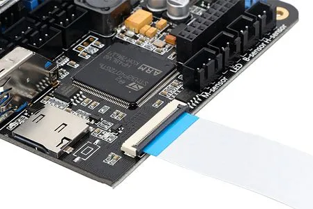
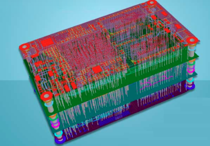
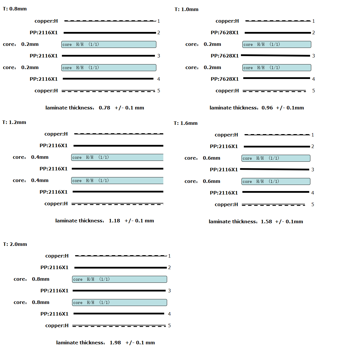
The core thickness range of HDI PCB (High Density Interconnect Circuit Board) mainly depends on its design and application requirements. According to different processes and application scenarios, the core thickness of HDI PCB can vary from 0.6mm to 1.0mm.
What is the standard thickness of a PCB core?
The standard thickness of PCB core boards usually includes the following specifications: 0.5mm, 0.7mm, 0.8mm, 1.0mm, 1.2mm, 1.5mm, 1.6mm, 2.0mm, 2.4mm, 3.2mm, 6.4mm. These thickness specifications are widely used in different electronic products and circuit board designs.
The thickness of PCB includes not only the thickness of the core board, but also the total thickness of all layers such as copper layer, solder mask layer and silk screen. The standard thickness ranges widely, from thinner 0.5mm to thicker 6.4mm, suitable for different application requirements.
Choosing the right PCB thickness is essential to ensure the performance and reliability of the circuit board. Thicker PCBs have higher mechanical strength and load-bearing capacity, and are suitable for products with high power and large electronic components, such as industrial, automotive, aerospace and military applications.
Ultra-thin PCBs are suitable for small electronic products such as smartphones, smart wearable devices and laptops due to their lightweight characteristics.
What is the thickness tolerance of a PCB core?
The thickness tolerance of a PCB core varies according to different thickness ranges.
For PCBs with a thickness of less than or equal to 1mm, the board thickness tolerance is ±10% of the board thickness. For example, a PCB with a thickness of 0.5mm has a tolerance of ±0.05mm; a PCB with a thickness of 0.8mm has a tolerance of ±0.08mm.
For PCBs with a thickness greater than 1mm and less than or equal to 1.6mm, the tolerance is ±0.14mm.
For PCBs with a thickness greater than 1.6mm and less than or equal to 2.0mm, the tolerance is ±0.18mm.
For PCBs with a thickness greater than 2.0mm and less than or equal to 2.4mm, the tolerance is ±0.22mm.
For PCBs with a thickness greater than 2.4mm and less than or equal to 3.0mm, the tolerance is ±0.25mm.
For PCBs with a thickness greater than 3.0mm, the tolerance is ±10%.
These tolerance standards apply to most PCB manufacturing processes, ensuring the stability and reliability of the PCB.
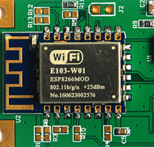
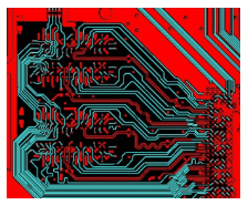
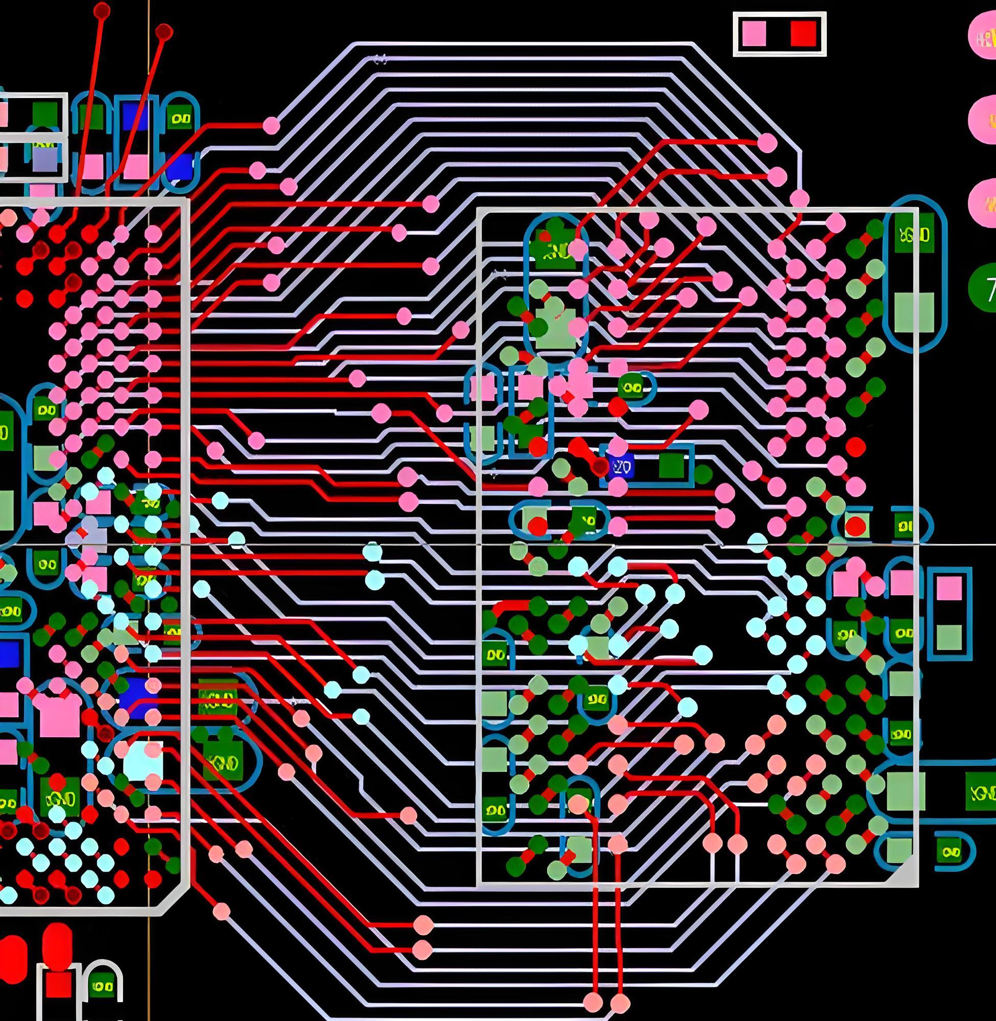
What is the difference between HDI and non-HDI PCB?
The main differences between HDI PCB and non-HDI PCB are their line density, size, production process and electrical performance. HDI PCB (High Density Interconnect PCB) has higher line density, smaller size and better electrical performance, while ordinary PCBs are lacking in these aspects.
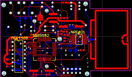
First of all, the design and structure of HDI PCB are significantly different from ordinary PCBs. HDI PCB adopts higher line density and more complex circuit layout, which enables smaller size and lighter design. In contrast, ordinary PCBs have lower line density and are suitable for some application scenarios that do not require high line density.
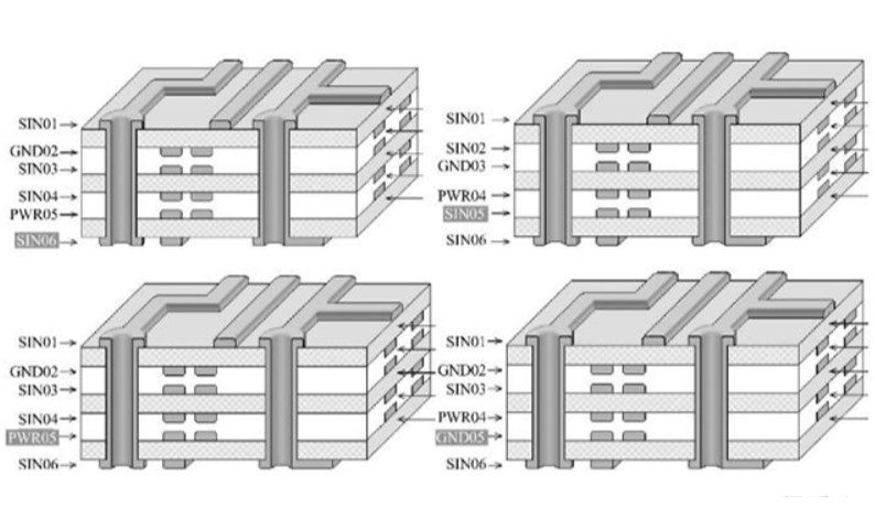
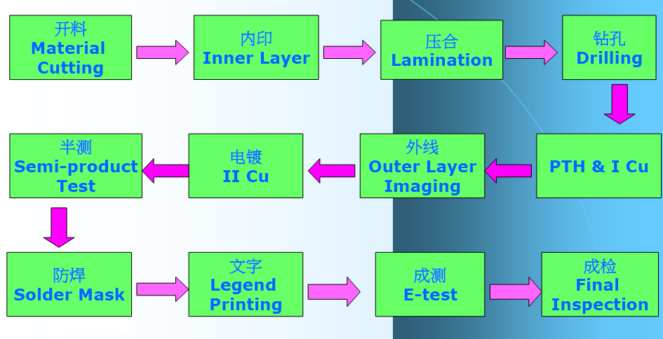
In terms of production process, the manufacturing process of HDI PCB is relatively complex, including laser drilling, stacked copper plates, etching technology, etc., to achieve high-density interconnection and complex circuit wiring. The manufacturing process of ordinary PCB is relatively simple, generally using photolithography, etching process, etc.
In terms of electrical performance, HDI PCB uses technologies such as blind holes and buried holes to reduce signal transmission paths and improve the transmission rate and stability of electrical signals. In addition, HDI PCB also has better radio frequency interference, electromagnetic wave interference, electrostatic discharge and thermal conductivity performance.
Finally, the cost of HDI PCB is relatively high, mainly due to its complex manufacturing process and high technical requirements. The manufacturing cost of ordinary PCB is low, which is suitable for some application scenarios with low requirements for line density and technology.
How thick is a 2 layer PCB core?
The thickness of a 2-layer PCB core is usually 0.4mm.
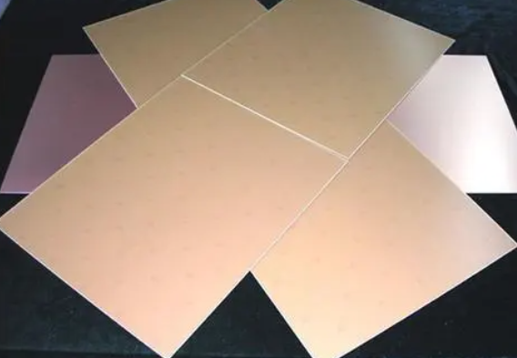
PCB core is a base material composed of copper foil, solid resin material and glass fiber, with a certain hardness and thickness. Common PCB core thickness specifications include 0.4mm, 0.5mm, 0.6mm, 0.7mm, 0.8mm, 1.0mm, 1.2mm, 1.5mm, 1.6mm, 2.0mm, 2.4mm, etc.
Among the common specifications of Shengyi core boards, the thickness of 0.4mm is widely used. In addition, the performance of multi-layer PCBs does not directly depend on the number of layers, but more reflects the space requirements during design.
Are HDI PCB reliable?
HDI PCBs are reliable. HDI PCBs are manufactured using high-density and high-reliability interconnection technology, with higher line density and more complex circuit layout, which can achieve smaller and lighter electronic devices.
Compared with ordinary PCBs, HDI PCBs perform well in anti-interference ability and electromagnetic compatibility, and can effectively reduce the impact of external interference on signal transmission, while having higher reliability and longer service life.
The reliability of HDI PCBs is due to the high-quality substrates, solder mask and copper foil materials used, as well as strict manufacturing processes and quality control. These characteristics enable HDI PCBs to maintain stable performance and quality in various harsh environments.
In addition, the development trend of HDI PCBs is towards higher integration, higher signal transmission rate, better electromagnetic compatibility and optimized thermal management capabilities, which further enhances its application value in high-performance and high-density integration requirements.
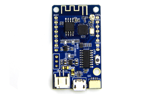
What are the benefits of HDI PCB?
The main benefits of HDI PCB include high-density wiring, high-performance signal transmission, adaptability to high-frequency applications, miniaturization, and thinness. These characteristics make HDI PCB play a vital role in electronic devices, especially in high-end electronic products such as smartphones, tablets, and high-end computers.
First, HDI PCB has the characteristics of high-density wiring, which can achieve more circuit connections in a smaller space. This allows the design of electronic products to be more compact and meet application scenarios with extremely high space requirements.
Secondly, HDI PCB excels in high-performance signal transmission, can provide better signal transmission quality and electrical performance, and is particularly suitable for processing high-speed and high-frequency signals.
In addition, HDI PCB also has the advantages of miniaturization and thinness, which contributes to the thinness and miniaturization of electronic products, making the equipment more portable while maintaining high performance.
These benefits of HDI PCB are due to its advanced manufacturing process and technology. By adopting finer line widths and smaller apertures, HDI PCB achieves higher wiring density and signal transmission speed.
At the same time, by optimizing material selection and circuit design, HDI PCB can reduce the loss and reflection during signal transmission and improve the integrity and accuracy of the signal. In addition, HDI PCB also has better anti-interference ability and electromagnetic compatibility, which can effectively reduce the impact of external interference on signal transmission.
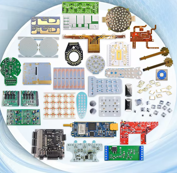
The application range of HDI PCB is very wide, including smart phones, tablets, laptops, medical equipment and communication equipment. Due to its high-density interconnection and excellent electrical performance, HDI PCB plays an important role in these fields, promoting the development of the PCB industry, so that more dense components can be arranged more closely on HDI boards.
What are the disadvantages of HDI PCB?
The main disadvantages of HDI PCB include high cost, complex production process, environmental sensitivity and possible quality problems.
First, the cost of HDI PCB is relatively high. This is because high-precision manufacturing technology and special materials are required in its manufacturing process, which all lead to its cost increase.
In addition, HDI PCB is usually used in high-performance equipment, and the value of these equipment itself is also high, which further pushes up the price of HDI PCB.
Second, the production process of HDI PCB is very complicated. Due to its high density of lines and components, the manufacturing of HDI PCB requires highly precise processes and equipment. This not only increases the difficulty of production, but may also lead to a longer production cycle, further increasing costs.
In addition, HDI PCB has certain requirements for the environment. Due to its delicate structure, HDI PCB is very sensitive to humidity and temperature changes in the environment. Improper storage or transportation conditions may cause the PCB to become damp or deformed, affecting its performance and reliability.
Finally, HDI PCB may have some quality problems. Due to the complexity of the production process, HDI PCB may have problems such as poor solderability, delamination, short circuit, open circuit, etc. These problems may need to be avoided through strict quality control and testing.
The core thickness of HDI PCB is an important parameter, which is directly related to the performance and application of PCB. When choosing the core thickness of HDI PCB, factors such as application requirements, design requirements and manufacturing process need to be considered comprehensively to select the appropriate core thickness.