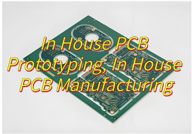
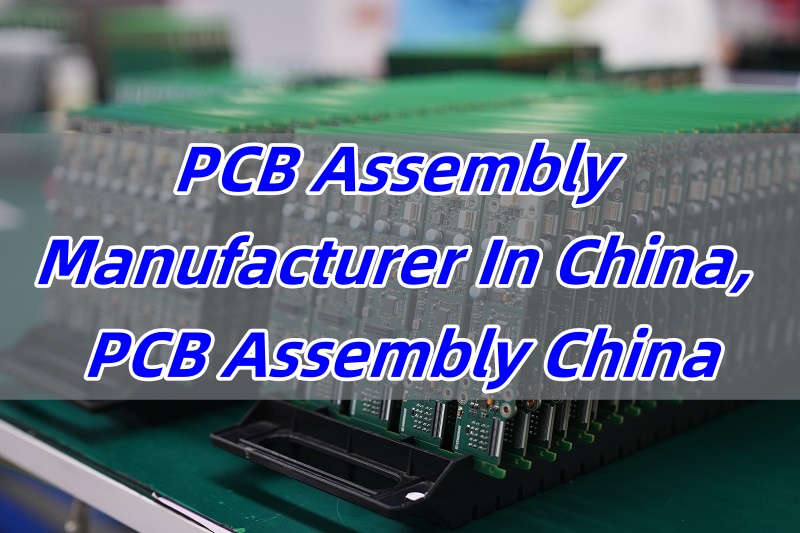
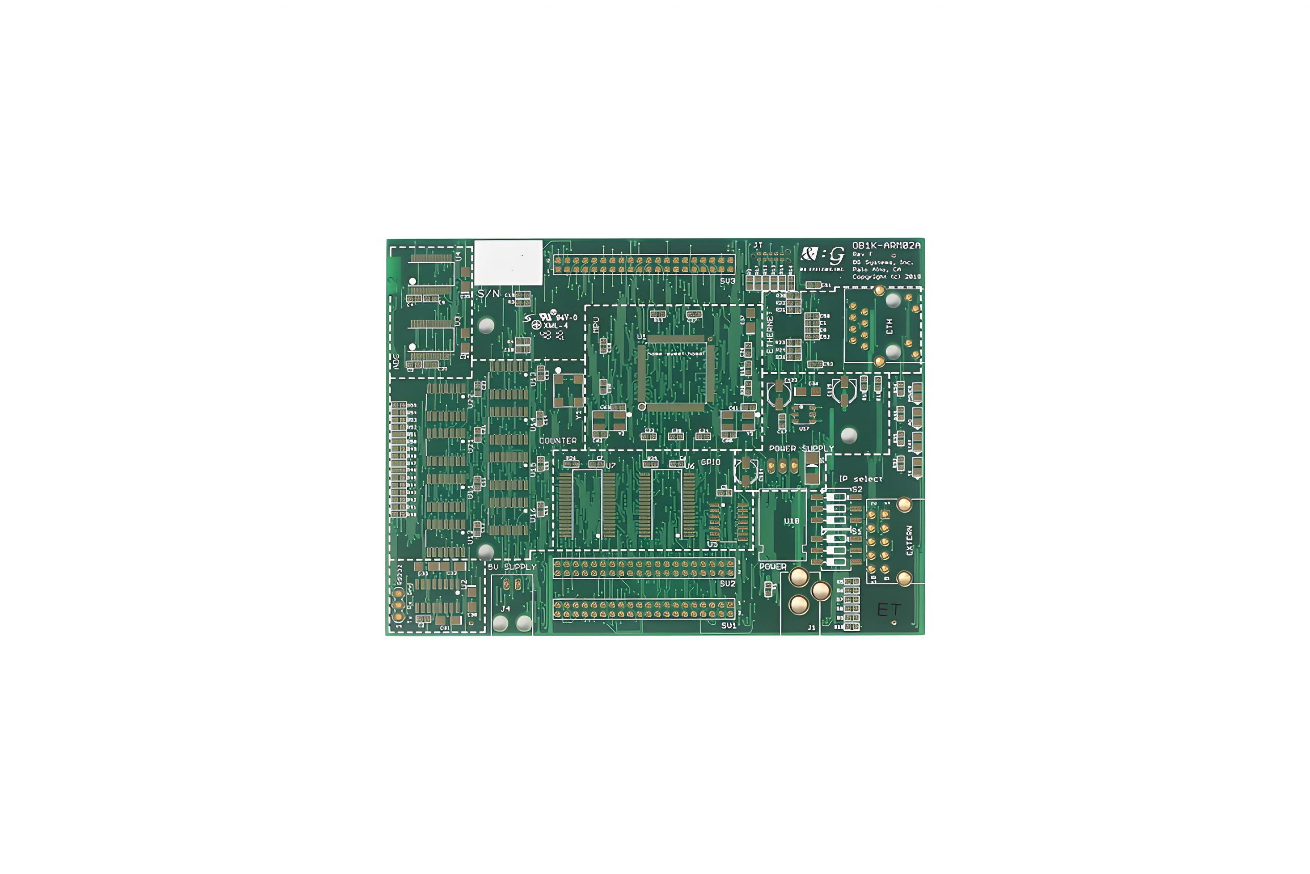
Quality PCB manufacturer in China is often the first choice for global buyers who seek a cost-effective yet reliable solution. While the market is full of suppliers, only a few truly understand what quality means from design to delivery. That’s where EBest Circuit (Best Technology) stands out.
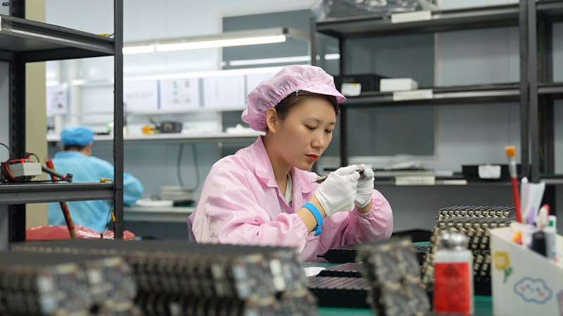
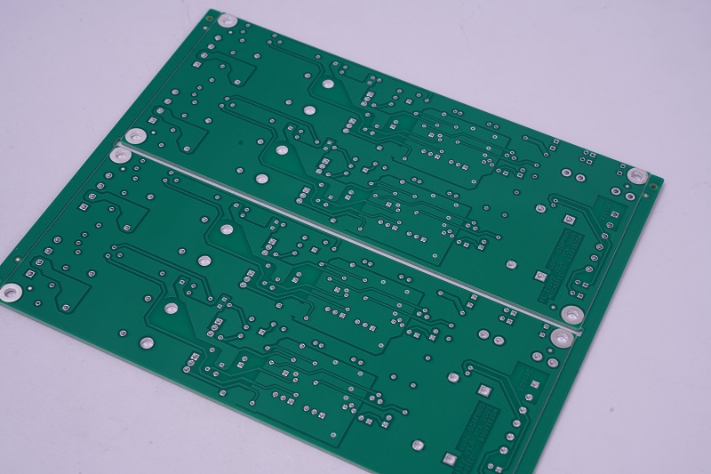
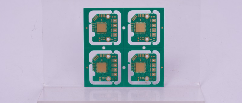
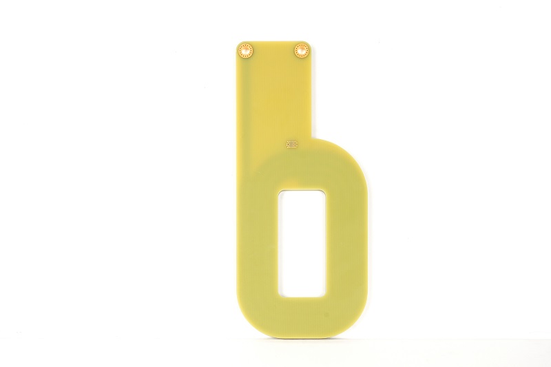
EBest Circuit (Best Technology) is a quality PCB manufacturer in China. Since 2006, EBest Circuit (Best Technology) has been down to do the quality PCB prototype, design, PCB manufacturing, and assembly. We perceive that quality PCB is the cornerstone for us to land the trust of our regular customers and the potential. Our factory complies with ISO 9001, ISO 13485, IATF 16949, and AS9100D certifications. Are you looking for a China PCB manufacturer? Please reach out to us at sales@bestpcbs.com for the best assistance with your projects. We are looking forward to having a business interaction with you and showing you around our PCB factory China in the near future.
Who Is the Quality PCB Manufacturer in China?
China has hundreds of PCB factories, but not all can meet international demands for consistency, transparency, and long-term cooperation. A quality PCB manufacturer in China should offer clear communication, timely delivery, and strong quality control. EBest Circuit (Best Technology) meets these needs with a comprehensive solutions and 19 years of practical experience. We understand what matters to engineers and purchasing teams alike.
Is EBest Circuit (Best Technology) Co., Limited a Chinese Company?
Yes, EBest Circuit (Best Technology) is a fully Chinese-owned company, but it operates with a global mindset. We serve customers from over 40 countries, combining local production with international expectations. This balance helps us deliver quality products at the right cost, backed by professional service and global logistics support.
Where Is EBest Circuit (Best Technology) Co., Limited Located?
We are based in Shenzhen, Guangdong, China’s electronics hub. Our location gives us easy access to raw materials, advanced equipment, and skilled workers. This also allows us to respond quickly to urgent orders and changing design requirements.
Who Is the Largest Manufacturer of Quality PCB in the US?
In the US, TTM Technologies is one of the largest quality PCB manufacturers. However, their costs and lead times are often higher compared to Chinese suppliers. Many American buyers choose to work with Chinese partners like EBest Circuit (Best Technology) for prototypes, small-batch, or volume runs due to better pricing and competitive turnaround times.
Who Is the Largest Quality PCB Manufacturer in the World?
Globally, companies like Zhen Ding Tech and Nippon Mektron lead the PCB industry by volume and technology. However, they mainly focus on massive production and are less flexible with small or custom orders. EBest Circuit (Best Technology) fills this gap by supporting both low-volume and high-mix projects while maintaining world-class standards.
How to Choose a Quality PCB Manufacturer in China?
When selecting a quality PCB manufacturer in China, consider the following:
- Design file support: The manufacturer must help review and correct design files, especially if layers or materials need optimization.
- Traceability system: Ensure they use MES or similar systems to track material.
- On-time delivery: Ask about their average lead time and strategies to avoid delays.
- Supplier chain strength: A strong network of verified material vendors can prevent shortages.
- Cost and stability: Pricing should be transparent, but also stable despite fluctuations in raw material costs.
- Post-sale support: A team that responds quickly to issues builds long-term trust.
Why Should You Choose EBest Circuit (Best Technology) as Your Quality PCB Manufacturer in China?
EBest Circuit (Best Technology) doesn’t just manufacture PCBs—we provide full quality PCB Solutions. Here’s what makes us different:
1. Verified Design File Support
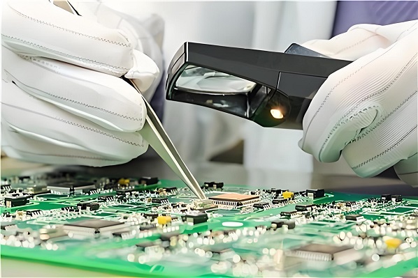
Many clients face errors in Gerber files or unclear stack-ups. Our engineering team checks every file, gives advice, and prevents avoidable failures before they happen. We work with customers from the design stage, not just during production.
2. Transparent Communication
We keep everything clear and updated. Our engineers, sales, and project managers speak fluent English and stay available across multiple time zones. You won’t feel left in the dark when production starts.
3. Flexible Scheduling and Reliable Delivery
Rush orders? Changing designs? No problem. We adjust schedules flexibly without compromising quality. Our smart planning tools and supplier reserves let us respond faster and deliver as promised.
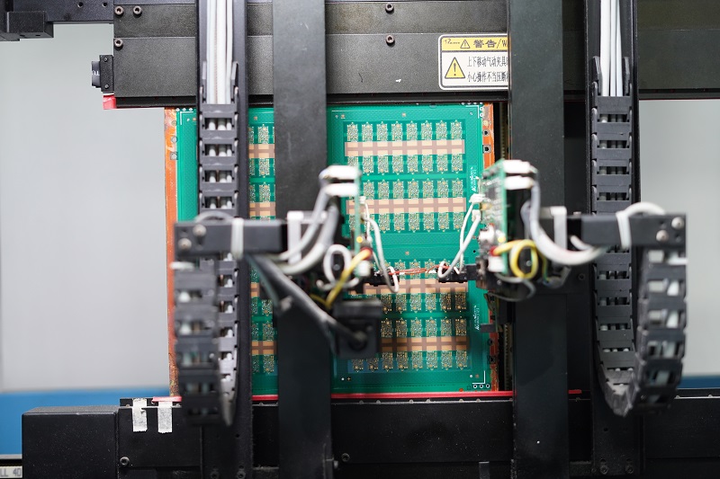
4. Full Traceability and Quality Control
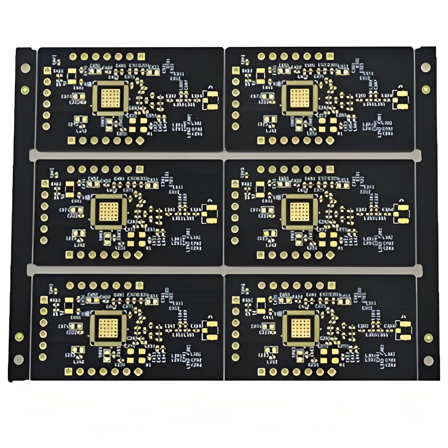
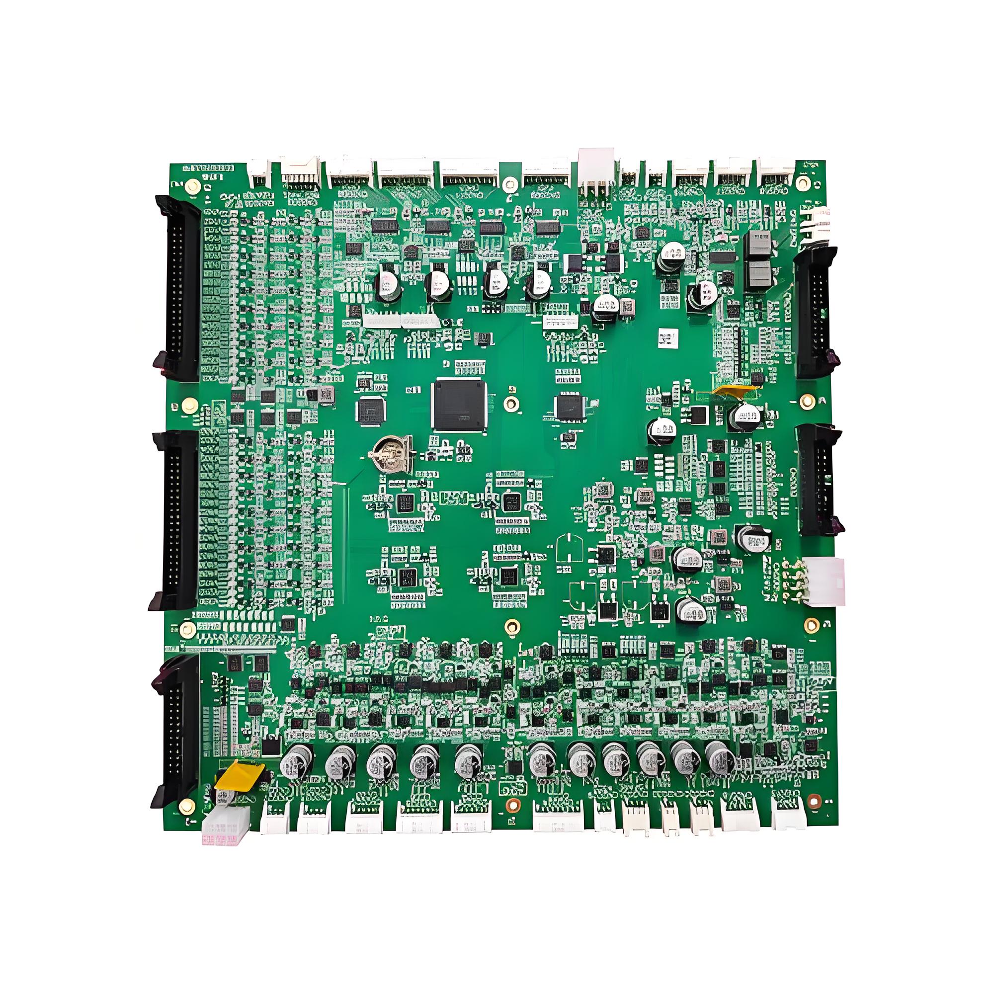
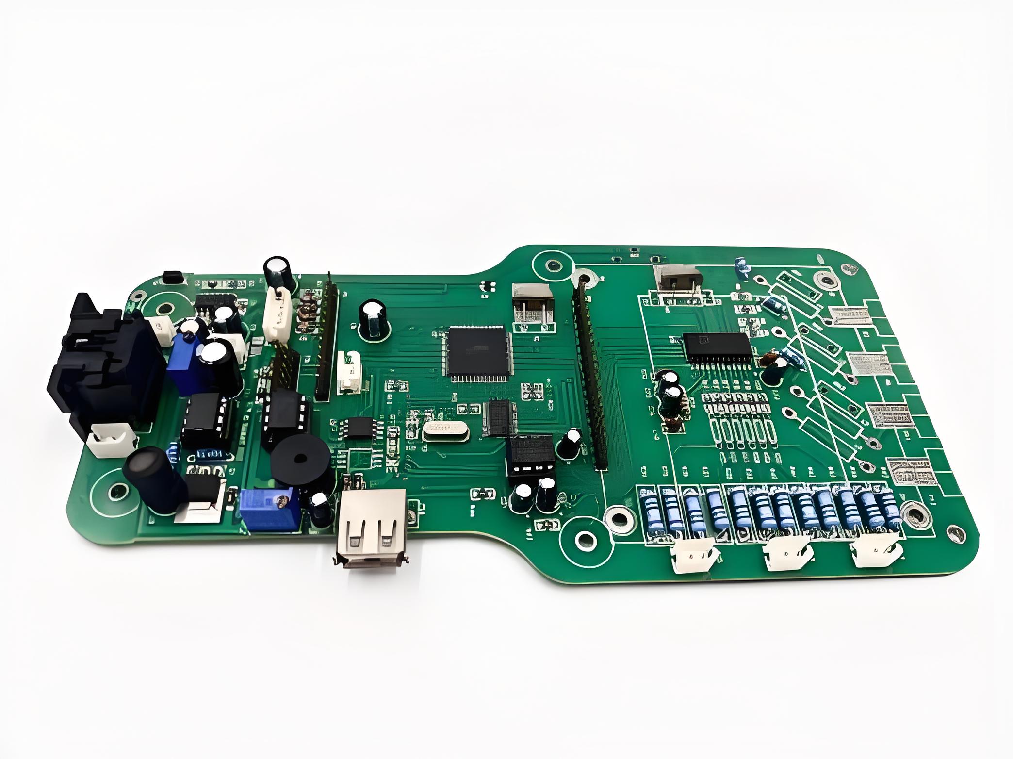
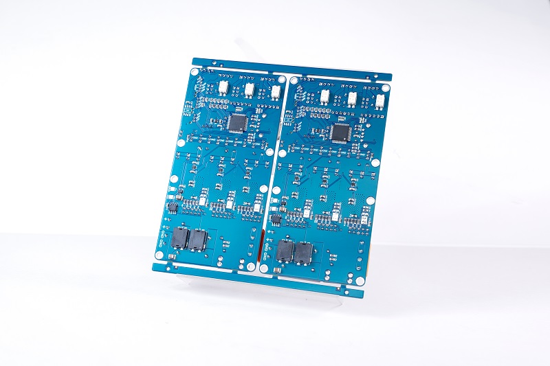
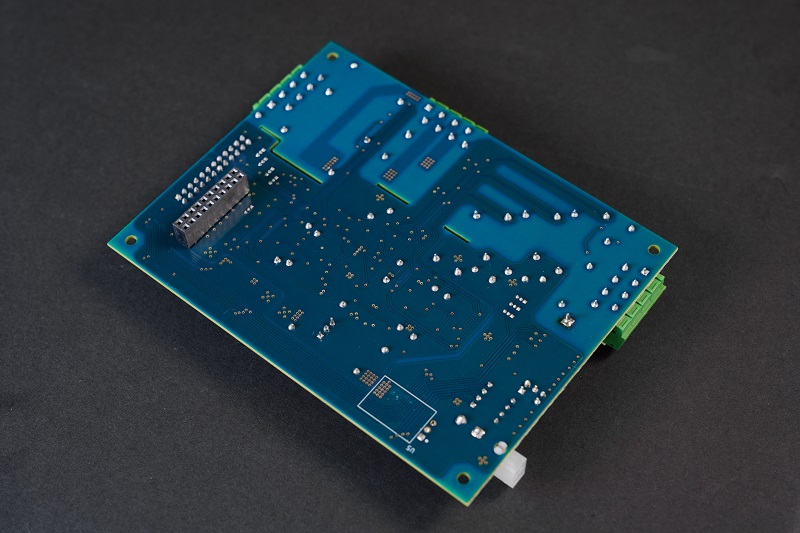
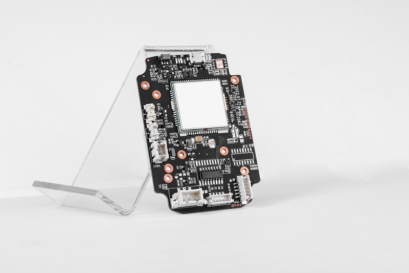
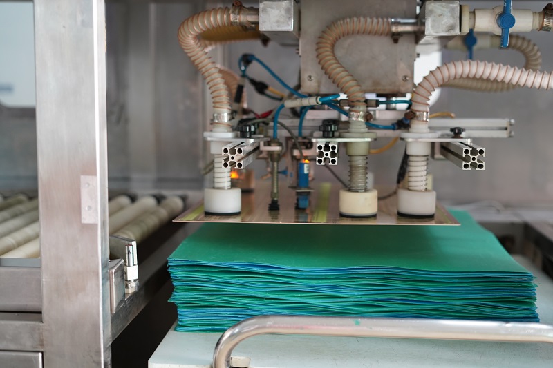
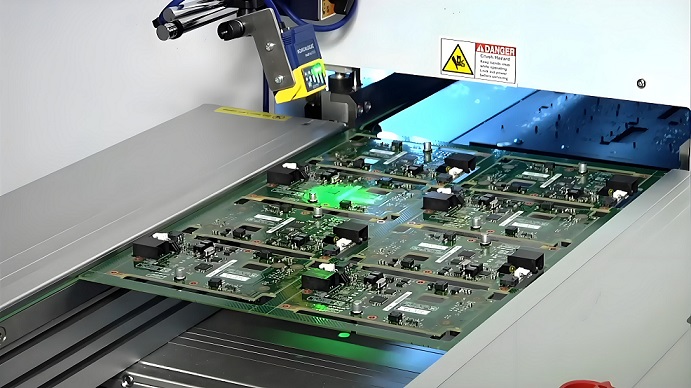
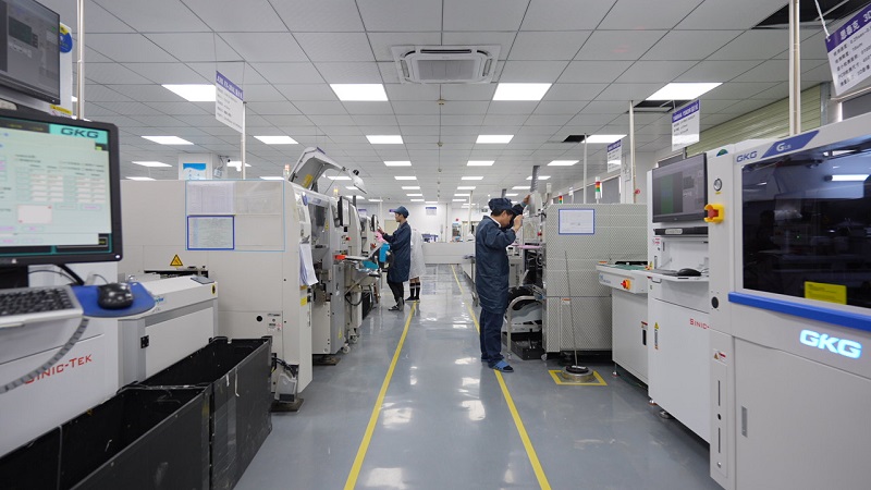
EBest Circuit (Best Technology) uses MES tracking and barcode labeling from raw materials to finished PCBs. Each board is fully traceable. We also apply AOI, X-ray, flying probe, and in-circuit testing for tight quality management.
5. Strong Supply Chain
Thanks to long-term partnerships with certified suppliers, we rarely suffer from material shortages. Even in times of high demand or logistics disruptions, we maintain stable production lines.
6. Cost Management Without Sacrificing Quality
We help you reduce costs by offering design-for-manufacturing advice and offering alternatives when materials are unavailable or too costly. Automation also helps us control labor costs and reduce waste.
7. Enhanced After-Sales and Localized Support
Our after-sales team follows up on every delivery. Whether it’s rework, replacement, or simply feedback—we respond within hours, not days.
To wrap things up, the demand for a quality PCB manufacturer in China is growing—but customers also demand better service, stronger quality control, and faster turnaround. EBest Circuit (Best Technology) understands these expectations. Our solutions address your project needs, ensuring you have no worries about design file errors, production delays, logistics issues, and poor traceability.
We combine clear communication, advanced technology, and human-centered service to give you a better experience from start to finish. For companies looking for dependable results, EBest Circuit (Best Technology) offers more than just a product—we offer a turnkey quality PCB solution. Feel free to contact us at sales@bestpcbs.com for our quick quote and professionalism.