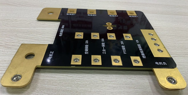
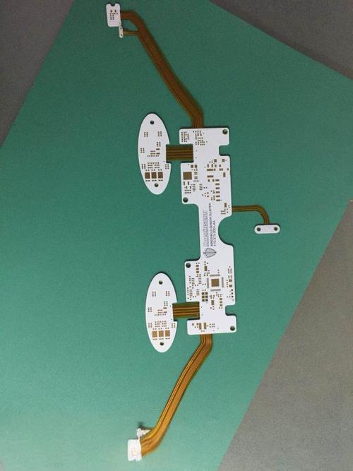
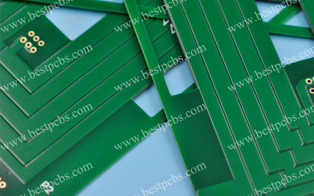
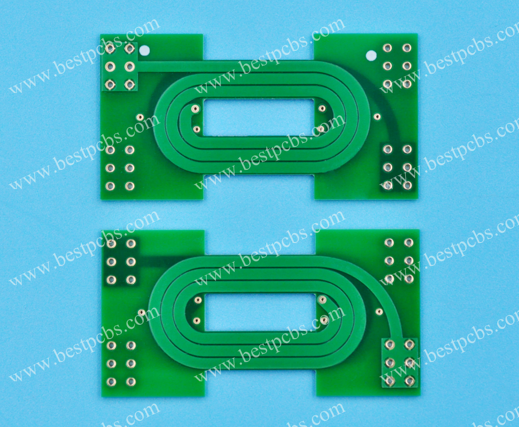
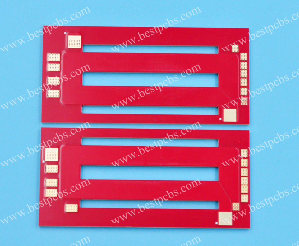
PCB board with high frequency laminate is a specialized printed circuit board designed to handle signals in the GHz range with minimal loss. Unlike standard FR-4 boards, it uses advanced laminate materials such as PTFE, ceramic-filled PTFE, or hydrocarbon composites to ensure low dielectric constant and low dissipation factor.

These properties allow the board to deliver stable electrical performance, maintain signal integrity, and reduce electromagnetic interference. High-frequency PCBs are essential in applications like 5G networks, radar systems, satellite communication, and RF devices, where even small signal distortions can impact overall performance.
Are you curious about EBest Circuit (Best Technology)’s pcb board with high frequency laminate?
- What is the maximum operating frequency and substrate type for high-frequency boards?
- What substrate/copper foil thicknesses are supported?
- What is the standard lead time?
EBest Circuit (Best Technology)’s pcb board with high frequency laminate can answer these questions.
- High-frequency boards use Rogers or Telfon substrates, and their frequencies typically range from 300MHz to 3GHz.
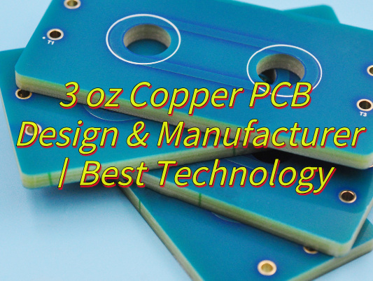
- Supported substrate thicknesses range from 0.5mm to 3.0mm (0.02″ to 0.12″), and copper foil thicknesses include 0.5oz, 1.0oz, 2.0oz, and 3.0oz.
- Sample delivery time is 7-9 days, and mass production (MP) lead time is 8-10 days.
What is the best PCB material for high-frequency?
Selecting the right PCB material is critical for high-frequency performance. It determines signal integrity, stability, and overall reliability. High-frequency circuits demand materials with low dielectric loss, stable thermal behavior, and minimal signal distortion.
The most popular materials for high-frequency boards include:
- PTFE (Polytetrafluoroethylene): Known for its low dielectric constant and excellent signal transmission.
- Rogers Laminates: A trusted brand offering laminates like RO3000 and RO4000 series for RF and high-speed designs.
- Ceramic-Filled PTFE: Provides improved mechanical strength and thermal performance compared to standard PTFE.
- Hydrocarbon Laminates: Offer a balance of cost-effectiveness and electrical properties for mid-frequency designs.
Each option has its benefits. PTFE remains the top choice for the highest frequency designs due to its superior electrical characteristics.
Hydrocarbon laminates are often chosen when cost and performance need balance. They work well for mid-range frequency designs while keeping costs lower than pure PTFE boards. The best material depends on your application.
Which materials have the highest frequency?
For extreme frequency applications, materials must maintain stable electrical characteristics under high speed. The dielectric constant (Dk) and dissipation factor (Df) must be low and consistent across the operating range.
- Rogers RO3003: Excellent for frequencies above 10 GHz.
- Taconic RF Series: Offers stable electrical performance for RF applications.
- Arlon Laminates: Known for thermal reliability and consistent performance.

These materials minimize signal degradation even at very high frequencies, making them essential for satellite, radar, and 5G applications.
Choosing these advanced laminates ensures your PCB can handle frequencies beyond 20 GHz without signal degradation.
What is considered high-frequency in PCB?
The term high-frequency refers to boards that handle signals above 300 MHz. However, in most cases, it applies to frequencies in the GHz range.
Digital systems often reach 50 MHz to 1 GHz. RF circuits start from 300MHz and go beyond 3 GHz. Microwave applications typically work between 20 GHz and 100 GHz.
As frequencies increase, material choice and design accuracy become more critical. Even minor variations in dielectric constant can cause signal delays or losses.
For designs above 1 GHz, standard FR-4 material is not suitable. High-frequency laminates are necessary to maintain performance and minimize interference.
What is the highest frequency PCB?
The highest frequency PCBs can support signals over 100 GHz. These boards are used in radar systems, satellite communication, and advanced wireless technologies.
Such boards require:
- Ultra-low Dk and Df materials
- Precise impedance control
- Advanced fabrication processes
PTFE-based laminates combined with ceramic fillers remain the standard for these extreme-frequency applications. Manufacturing these boards demands strict process control. Small errors in thickness or copper roughness can affect performance significantly.
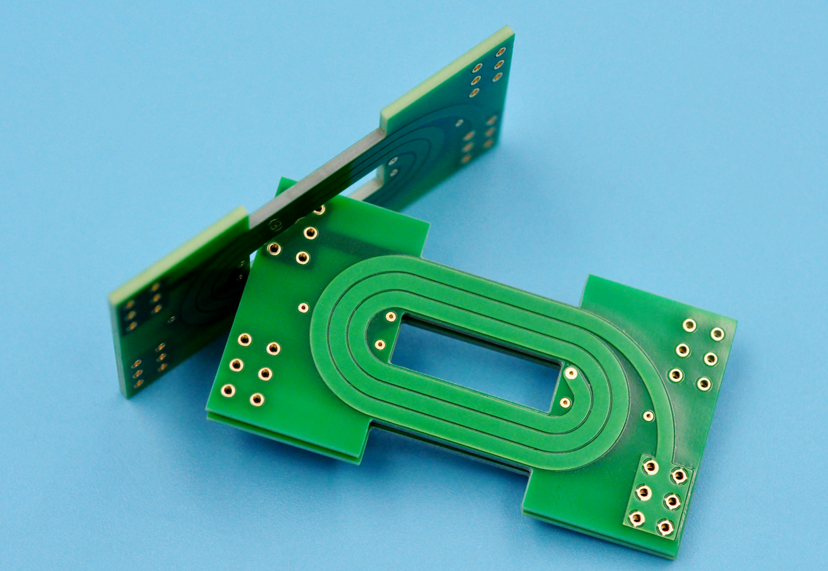
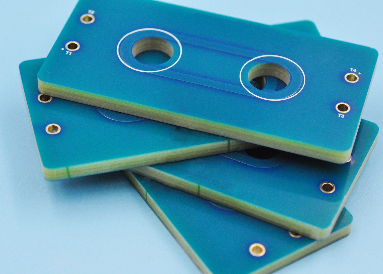
What is lamination in PCB?
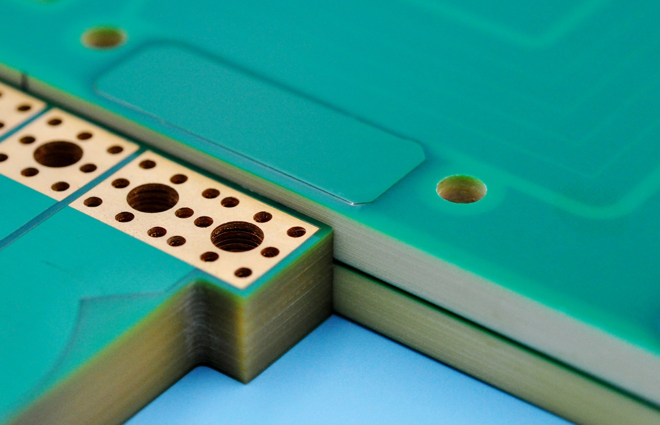
Lamination is the process of bonding copper layers to dielectric materials under heat and pressure. It forms the multilayer structure of a PCB.
In high-frequency boards, lamination is even more critical. It must ensure consistent thickness, strong adhesion, and zero defects.
The process affects electrical performance, especially impedance control. Incorrect lamination can cause air gaps or uneven layers, which impact signal transmission.
High-quality lamination keeps your board reliable under high-speed operation. It ensures smooth copper surfaces, accurate layer alignment, and long-term durability.
How to design a high-frequency PCB?
Designing a PCB board with high frequency laminate requires attention to detail. Here are the core steps:
- 1. Choose the Right Laminate
Select a material with low Dk, low Df, and stable thermal properties.
- 2. Control Impedance
Use proper trace widths and spacing to maintain impedance.
- 3. Reduce Crosstalk
Keep high-speed signals away from each other. Add ground planes when possible.
- 4. Minimize Signal Loss
Avoid unnecessary vias. Use smooth copper to reduce attenuation.
- 5. Consider Stack-Up
A well-planned layer stack-up improves performance and reduces EMI issues.

How to reduce electromagnetic interference in PCB?
Electromagnetic interference (EMI) can degrade the performance of high-frequency circuits. Here’s how to reduce it:
- Add Ground Planes: They provide a return path and reduce noise.
- Use Shielding: Metal enclosures or conductive coatings can block external interference.
- Shorten Signal Paths: Long traces act as antennas and increase EMI.
- Filter Power Lines: Use decoupling capacitors to reduce noise on power rails.
- Maintain Proper Spacing: Keep noisy and sensitive components apart.
Following these steps ensures a clean signal and improves board reliability. These techniques keep your board stable and interference-free.
What is the difference between high-speed and high-frequency PCB?
High-speed and high-frequency PCBs are different, though often confused.
- High-Speed PCB: Refers to fast digital signals with sharp rise times, typically in MHz or low GHz.
- High-Frequency PCB: Focuses on RF and microwave signals, often above 1 GHz.
The main difference lies in signal type and frequency range. High-speed boards emphasize signal integrity for digital data, while high-frequency boards handle analog signals like RF transmissions.
When should you use high-frequency?
You should choose a high-frequency PCB when your application works in the GHz range. These boards are essential for wireless communication, radar, and RF systems.
Use high-frequency PCBs for devices like smartphones, Wi-Fi routers, and 5G base stations. They are also required in satellite equipment, medical imaging systems, and automotive radar.

Any application needing low signal loss, stable impedance, and consistent performance at high speed requires these boards.
Standard FR-4 materials cannot provide the stability needed at these frequencies. High-frequency laminates are the only reliable choice.
If you need expert solutions for high-frequency PCBs, contact us at sales@bestpcbs.com. Our team is ready to provide professional support and the best quality boards for your application.