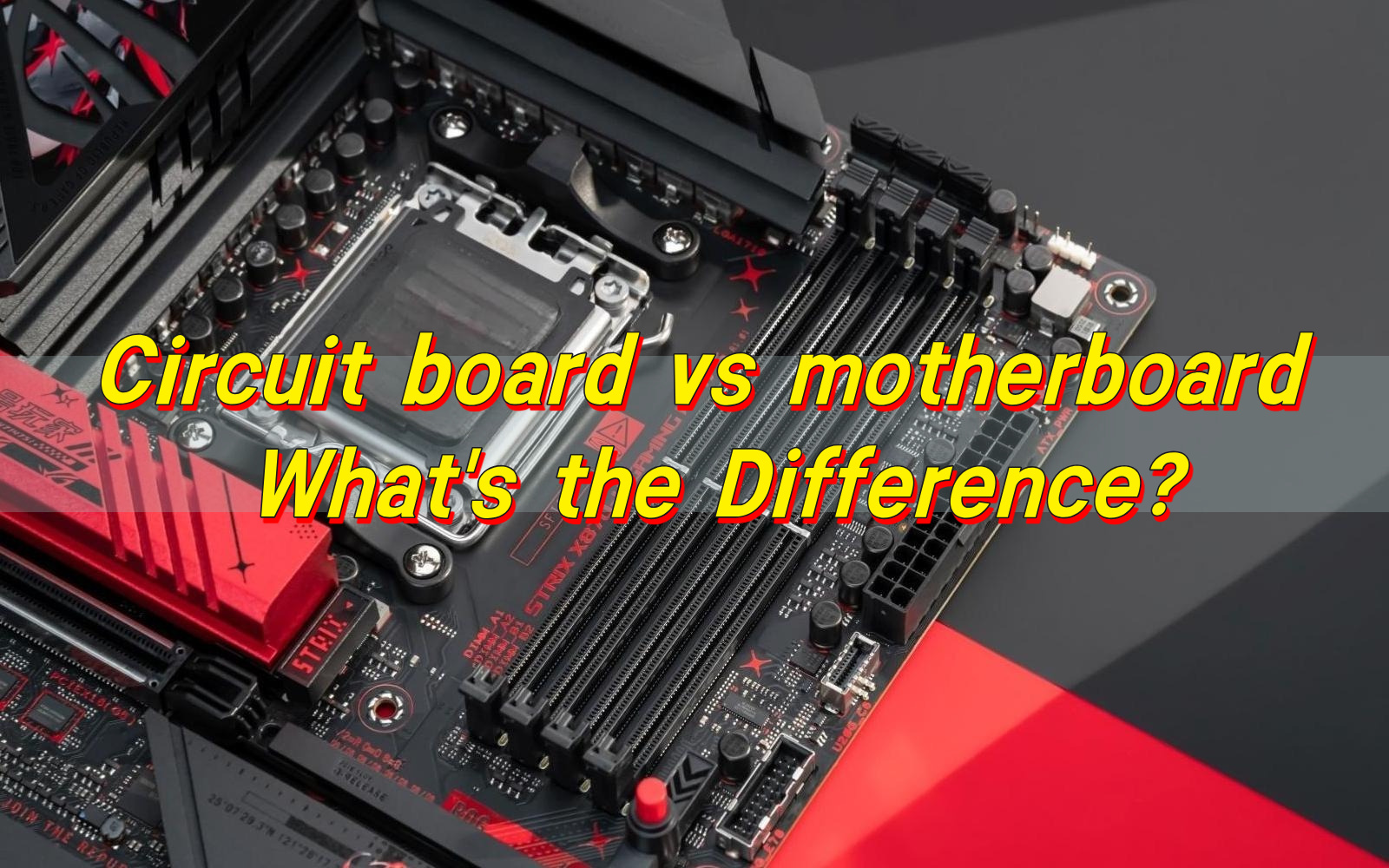
Circuit board vs motherboard is a common comparison, but the two terms are not interchangeable. A circuit board is the basic platform that holds and connects electronic components using copper traces. It is used in almost every electronic product, from simple controllers to complex industrial equipment.
What is a Circuit Board?
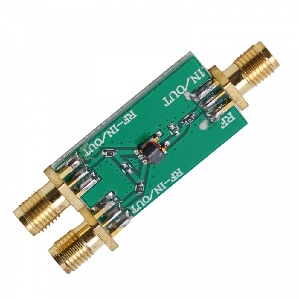
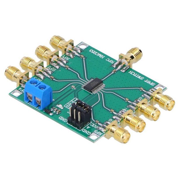
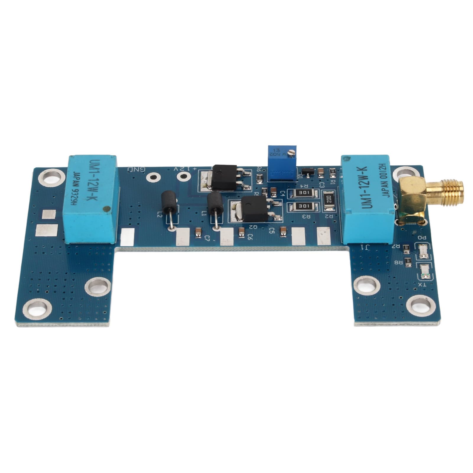
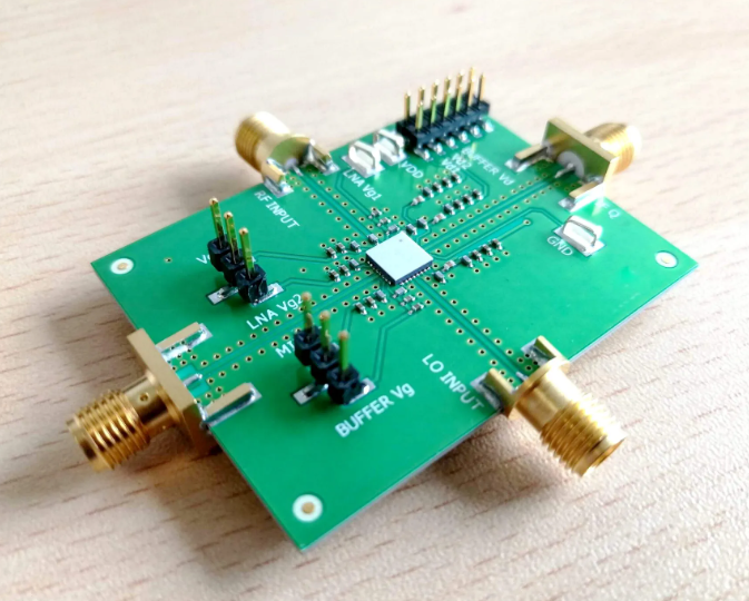
Circuit board is the physical platform that supports and connects electronic components. It provides mechanical stability, electrical pathways, and thermal management for an electronic system. Copper traces etched or printed onto an insulating base material form the conductive routes that allow current and signals to flow between components.
Circuit board is not a finished product by itself. It is a foundation. Components such as resistors, capacitors, integrated circuits, and connectors are mounted onto the board through surface-mount or through-hole methods. Once assembled, the board becomes a functional electronic unit.
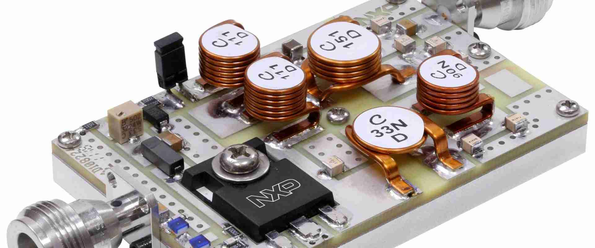
In practical manufacturing terms, a PCB board serves several purposes at the same time. It ensures reliable electrical connections, keeps component placement organized, and improves consistency in mass production.
From consumer electronics to industrial automation, circuit boards are everywhere. You will find them inside power supplies, LED lighting, medical monitors, automotive controllers, and communication equipment.
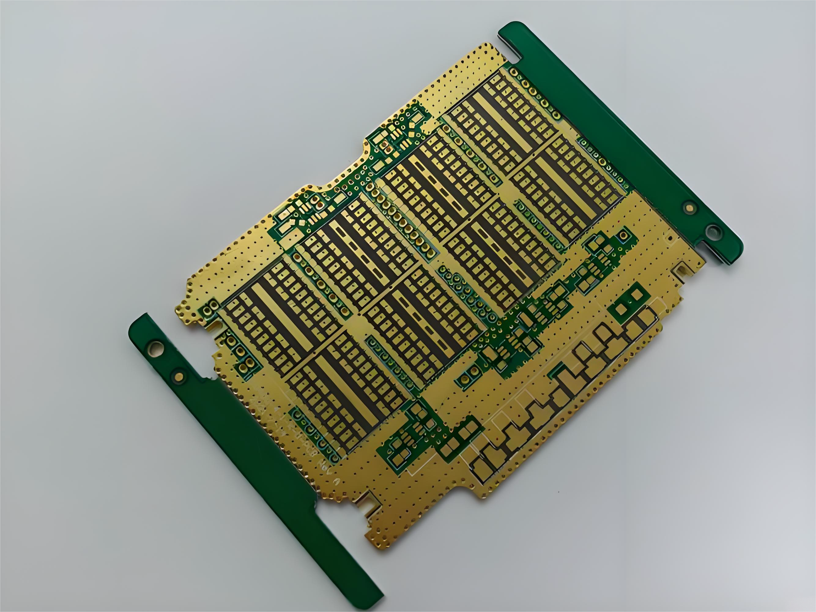
At EBest Circuit (Best Technology), circuit boards range from basic two-layer boards to advanced HDI structures. Each design is tailored to its electrical load, signal speed, and operating environment.
What are the different types of circuit boards?
Circuit boards are not all built the same way. Their structure, material, and complexity vary based on application needs.
Common types of circuit boards include:
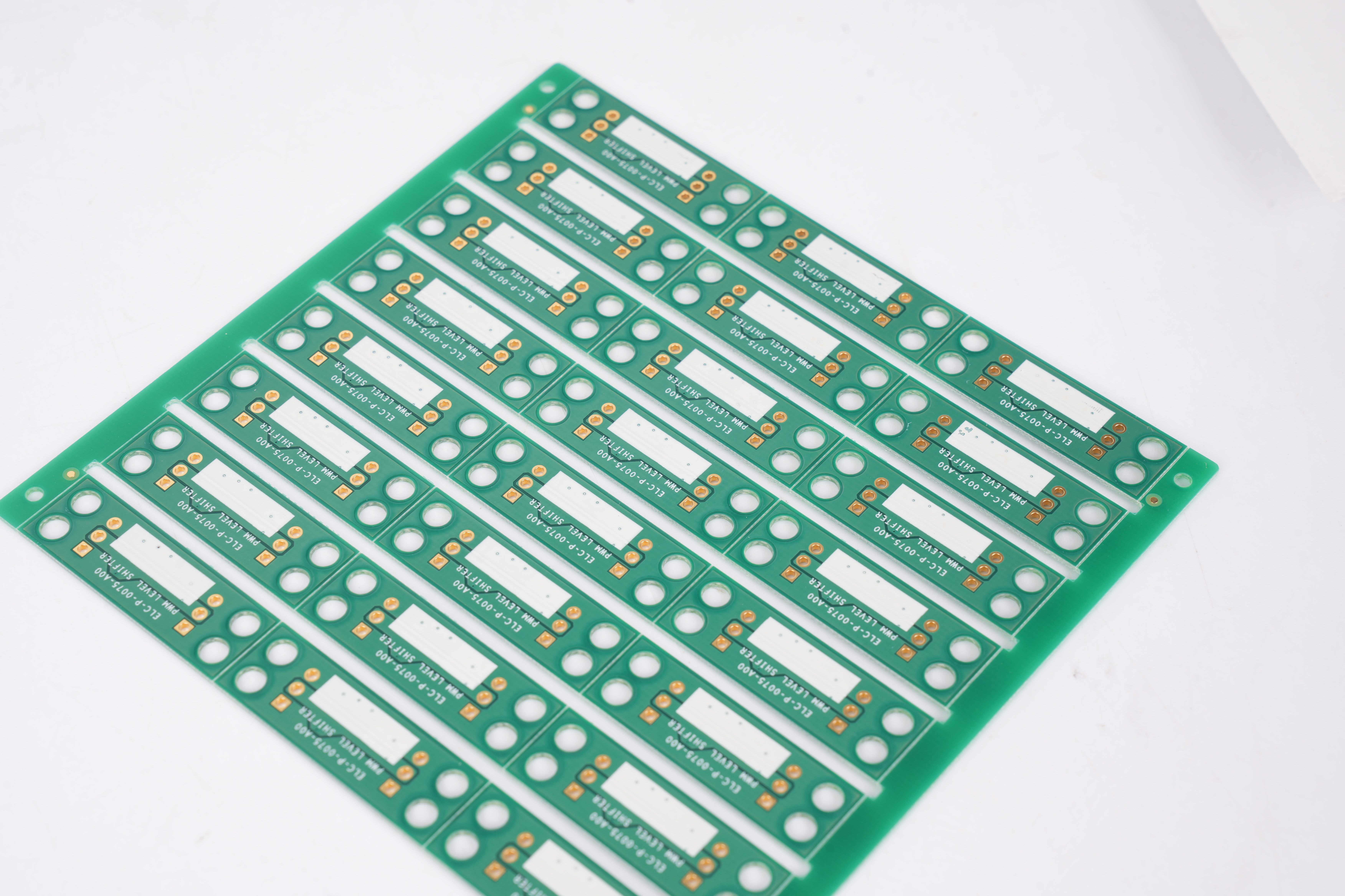
- Single-layer circuit boards: These boards have copper on only one side. They are simple, low cost, and widely used in basic electronics such as toys, adapters, and simple control modules.
- Double-layer circuit boards: Copper exists on both sides of the substrate. Vias connect the two layers. This design allows higher component density and more routing flexibility.
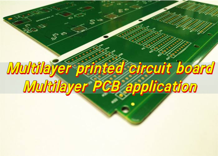
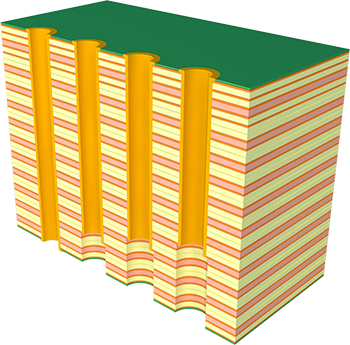
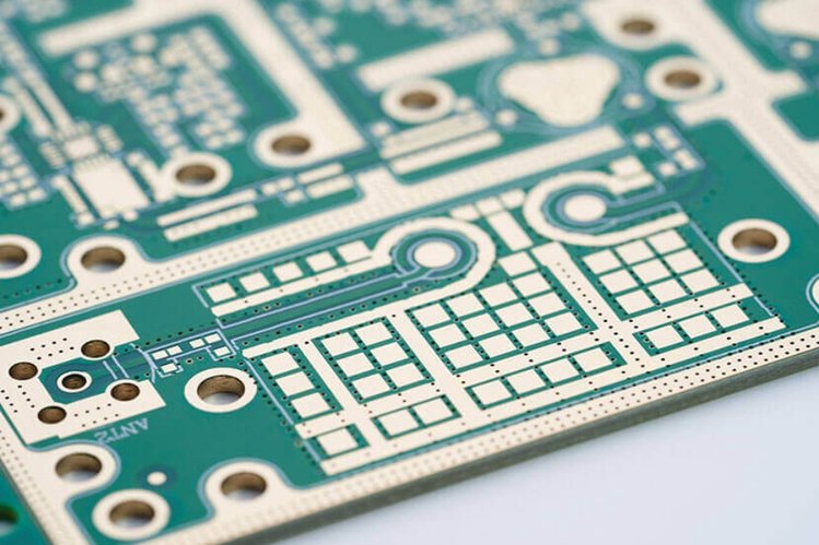
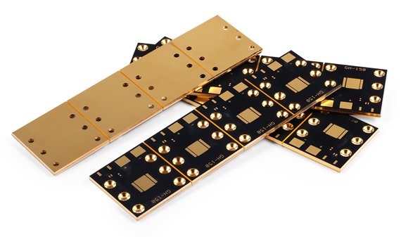
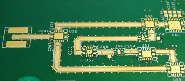
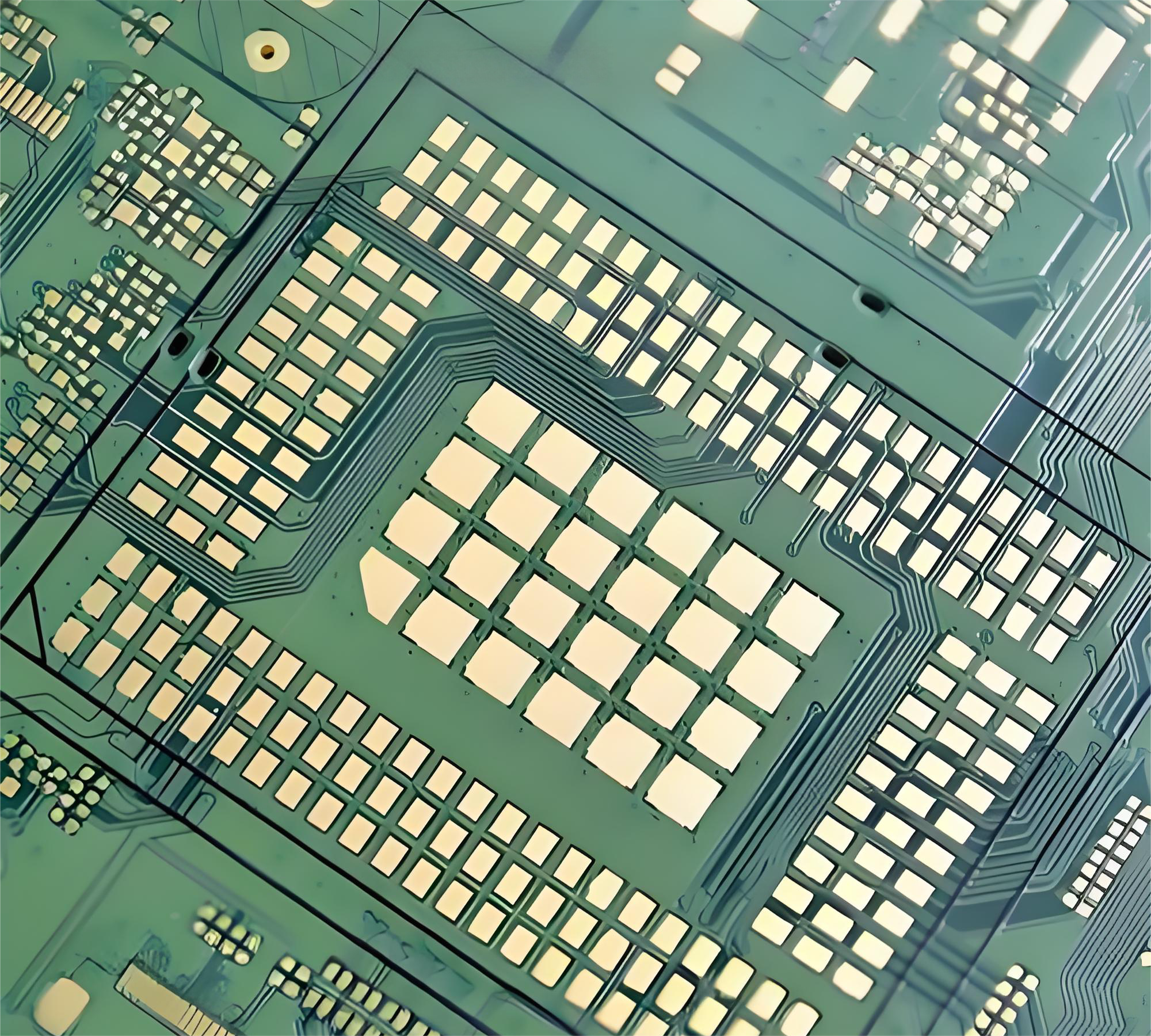
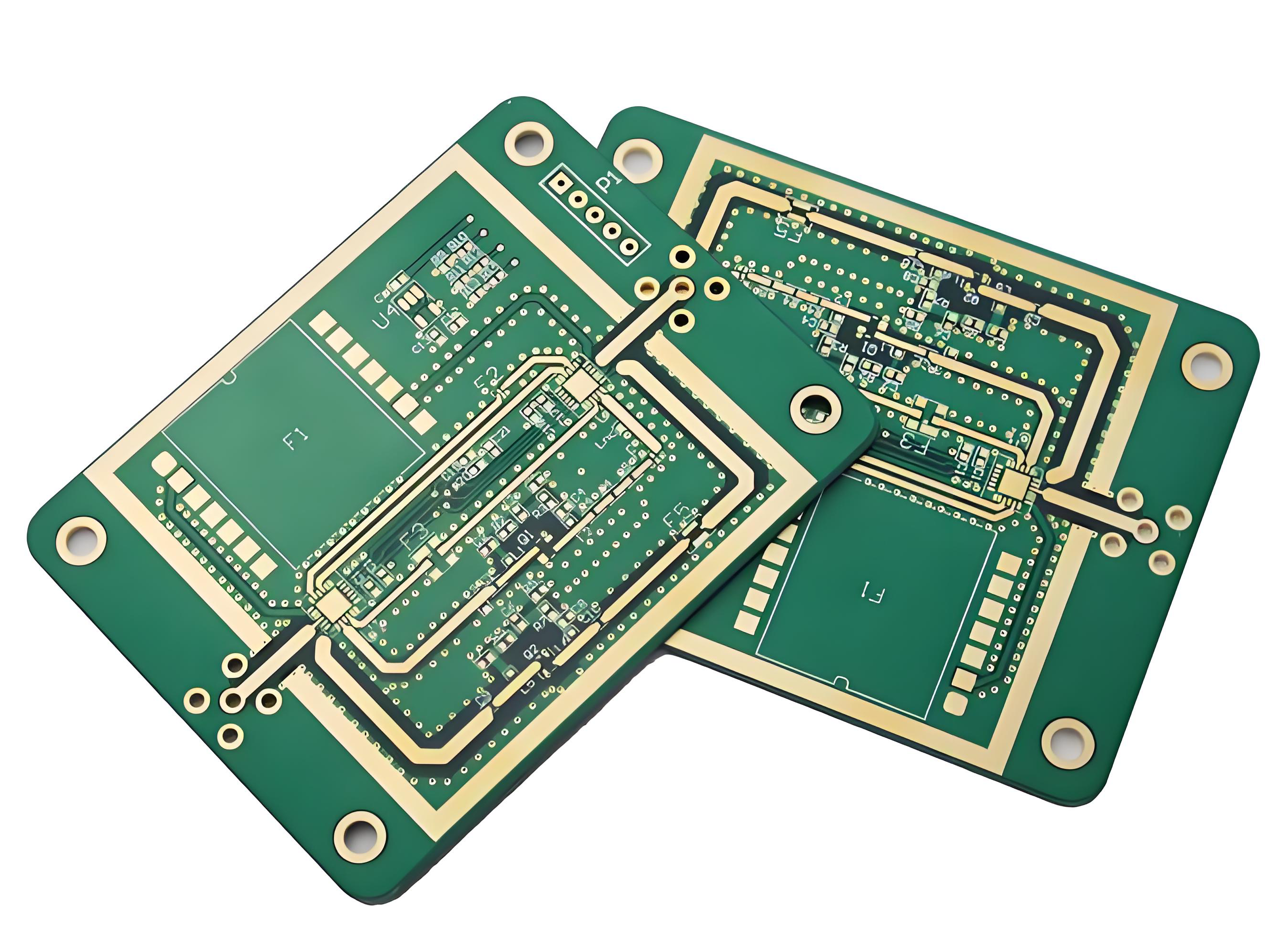
- Multilayer circuit boards: These boards contain three or more copper layers stacked with insulating material in between. They support complex routing, controlled impedance, and stable power distribution.
- Rigid circuit boards: Made from materials like FR-4, rigid boards hold their shape. They dominate most electronics applications.
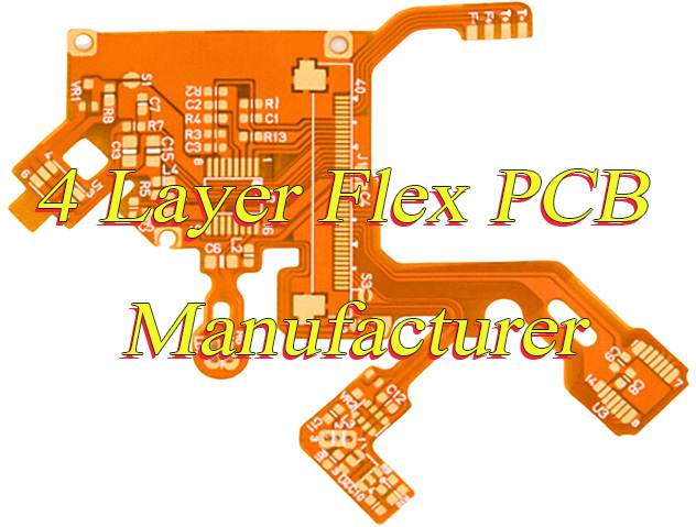
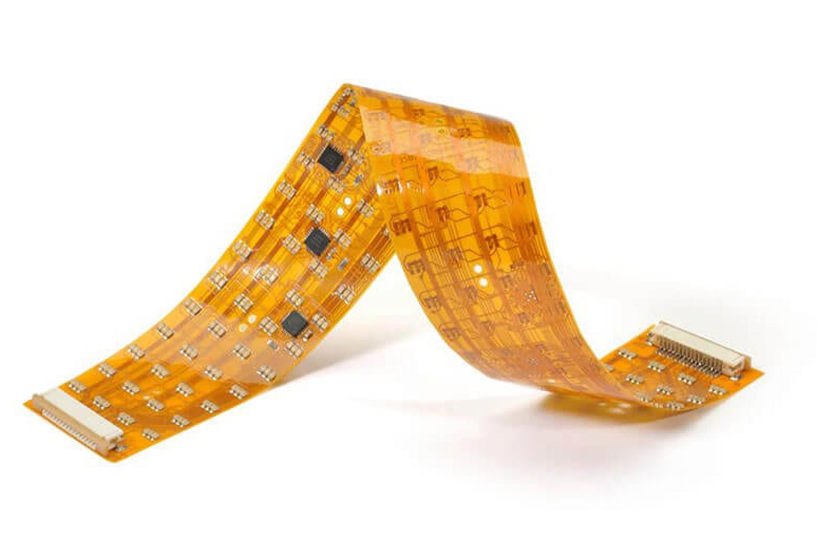
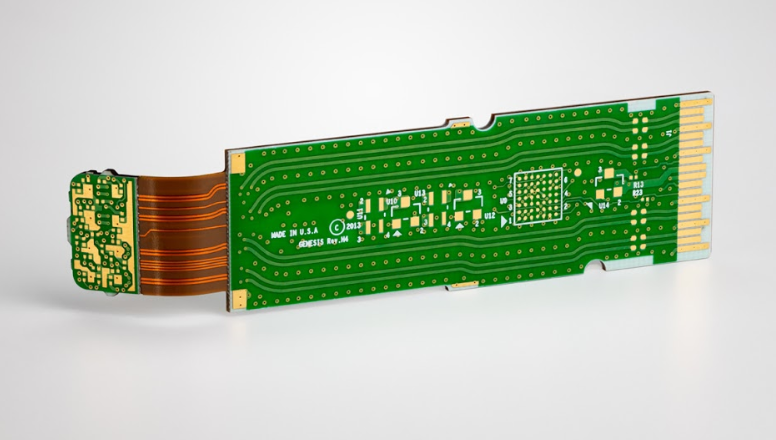
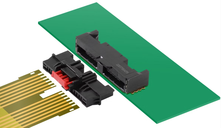
- Flexible circuit boards: Built on polyimide films, these boards bend and fold. They are common in cameras, wearables, and compact consumer devices.
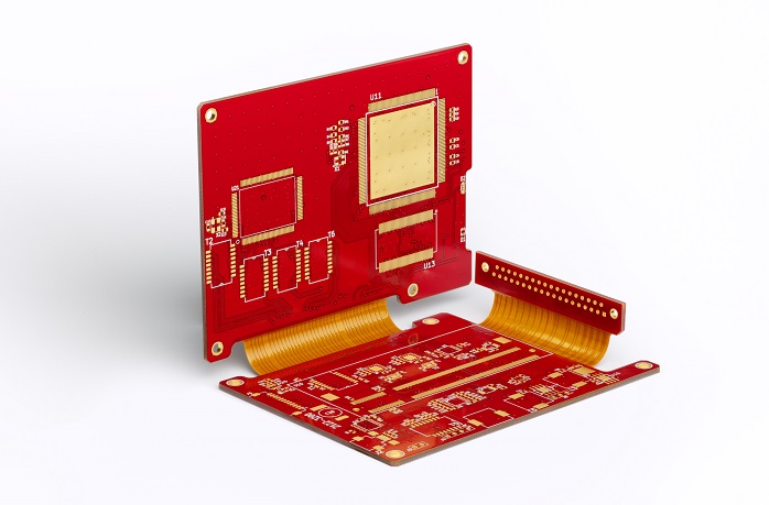
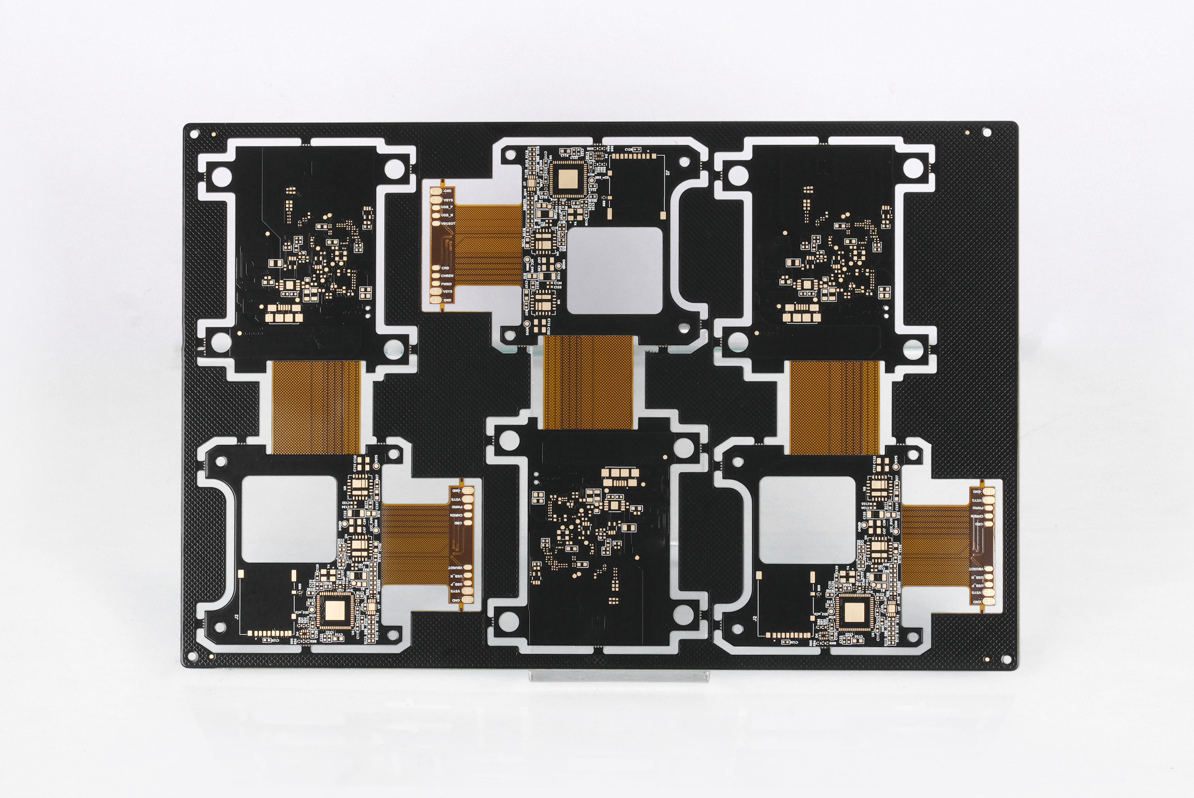
- Rigid-flex circuit boards: A hybrid of rigid and flexible sections. They reduce connectors and improve reliability in space-constrained designs.
Each of these is still a circuit board. A motherboard belongs to this family, but with a very specific role and structure. EBest Circuit (Best Technology) manufactures all of these PCB board types, adjusting stack-ups, copper thickness, and surface finishes to match functional demands.
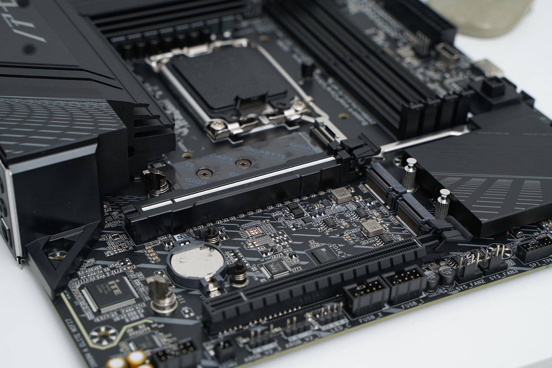
What is a Motherboard?
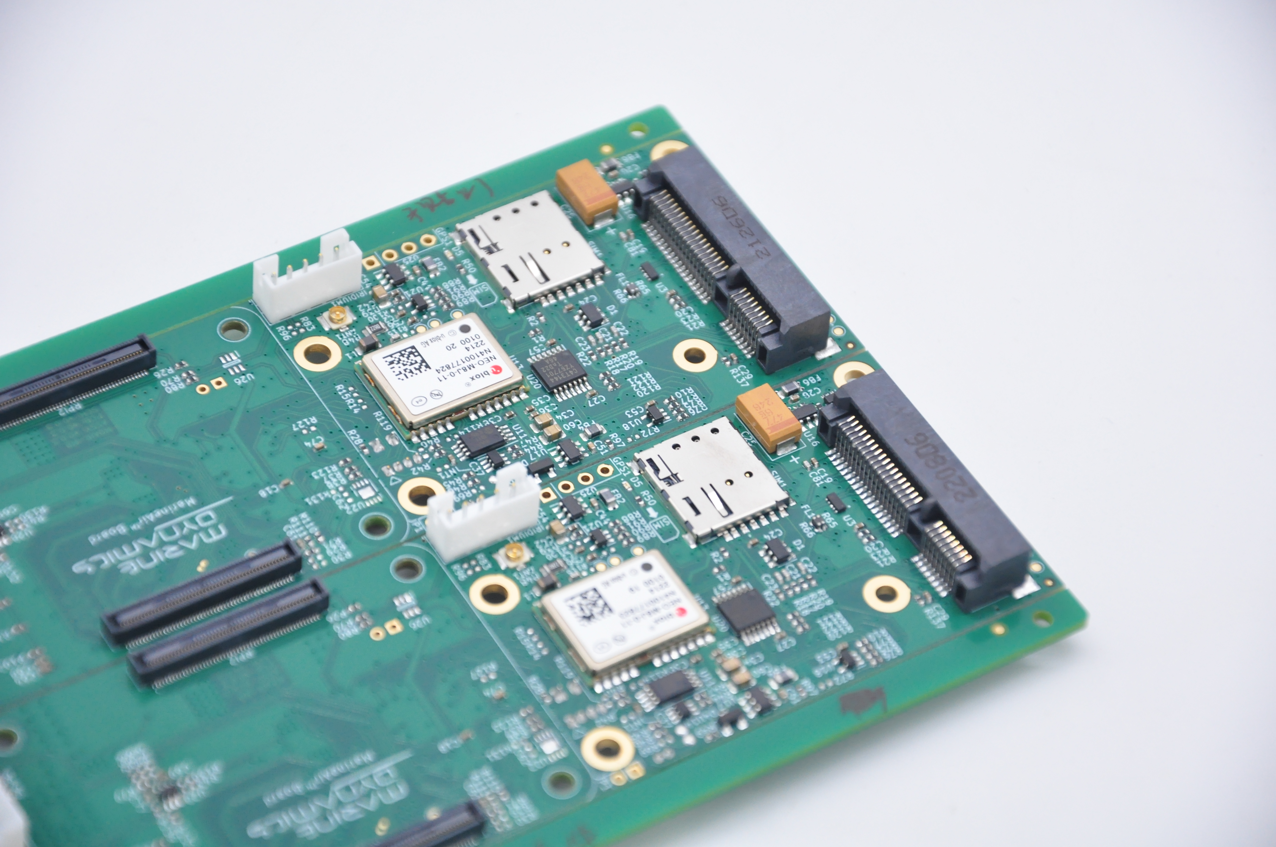
Motherboard is a specialized and highly integrated type of circuit board. Its primary function is to act as the central connection hub of an electronic system. Unlike simpler PCB boards that serve one function, a motherboard coordinates multiple subsystems at once.
In a computer or embedded system, the motherboard hosts the main processor, memory interfaces, power regulation circuits, and communication buses. It allows different modules to talk to each other through well-defined electrical pathways.
The term “motherboard” originated in computing, but today it extends beyond desktop PCs. Industrial controllers, medical devices, networking equipment, and even automotive control units can have motherboard-style PCBs. In these cases, the board may not resemble a PC motherboard visually, but the architectural role is similar.
Motherboards usually demand tighter tolerances, higher layer counts, and stricter signal integrity control. Power delivery and grounding must be carefully planned. Small layout mistakes can cause noise, instability, or overheating.
EBest Circuit (Best Technology) often supports customers who move from simple PCB boards to full motherboard designs as their products mature. This transition requires deeper engineering coordination and manufacturing discipline, especially for multilayer stack-ups and high-speed signals.
What are the different types of Motherboards?
Just as circuit boards come in many forms, motherboards also vary by application and scale.
Typical motherboard types include:
- Desktop computer motherboards: These boards support CPUs, RAM slots, graphics cards, storage interfaces, and peripheral connectors.
- Server motherboards: Designed for reliability and continuous operation. They support multiple processors, large memory capacity, and advanced power management.
- Embedded system motherboards: Used in industrial machines, medical devices, and automation systems. They focus on stability, long lifecycle, and specific I/O requirements.
- Industrial control motherboards: These boards operate in harsh environments. They may include reinforced power circuits, wider temperature tolerance, and thicker copper layers.
In all cases, the motherboard PCB layers are carefully engineered to balance signal routing, power planes, and thermal paths. EBest Circuit (Best Technology) frequently works on custom motherboard PCB projects where off-the-shelf solutions do not meet performance or size requirements.
Is the motherboard the same as the circuit board?
The short answer is no, they are not the same, but they are closely related.
A motherboard is a circuit board, but not every circuit board is a motherboard. The distinction is functional rather than material. A circuit board can perform a single task, such as voltage regulation or signal conversion. A motherboard integrates many tasks and coordinates system-level operation.
Think of a circuit board as a component, and a motherboard as a system platform. The motherboard often contains or connects to multiple other PCB boards. These may include daughter boards, expansion cards, or functional modules.
What is the difference between motherboard and circuit board?
From a design standpoint, a circuit board usually focuses on one function. It may amplify a signal, convert power, or control a motor. A motherboard must support many functions at once and ensure they work together without interference.
From a structural standpoint, motherboards often require more layers. High-speed data lines, stable power planes, and controlled impedance routing are common. A simple PCB board may only need one or two layers.
From a manufacturing standpoint, motherboard production involves tighter inspection standards. Layer alignment, impedance testing, and thermal reliability become critical. At EBest Circuit (Best Technology), motherboard PCB projects often go through additional design-for-manufacturing checks before fabrication begins.
Another practical difference lies in lifecycle expectations. Motherboards are expected to last longer and support firmware updates or hardware revisions. Circuit boards used as submodules may be replaced or redesigned more frequently.
How does PCB motherboard design work?
PCB motherboard design is a structured and disciplined process. It starts with system architecture rather than component placement.
The design process typically includes several coordinated steps. Engineers first define functional blocks and interfaces. They then allocate PCB motherboard layers for power, ground, and signals.
Component placement follows strict rules. Processors, memory, and power circuits are positioned to minimize noise and heat. Decoupling capacitors are placed close to critical pins.
Once routing is complete, simulation and verification take place. Signal integrity, power integrity, and thermal behavior are analyzed.
EBest Circuit (Best Technology) supports this process by providing early feedback on stack-up feasibility, copper weight selection, and drilling limits. This collaboration reduces rework and speeds up time to production.
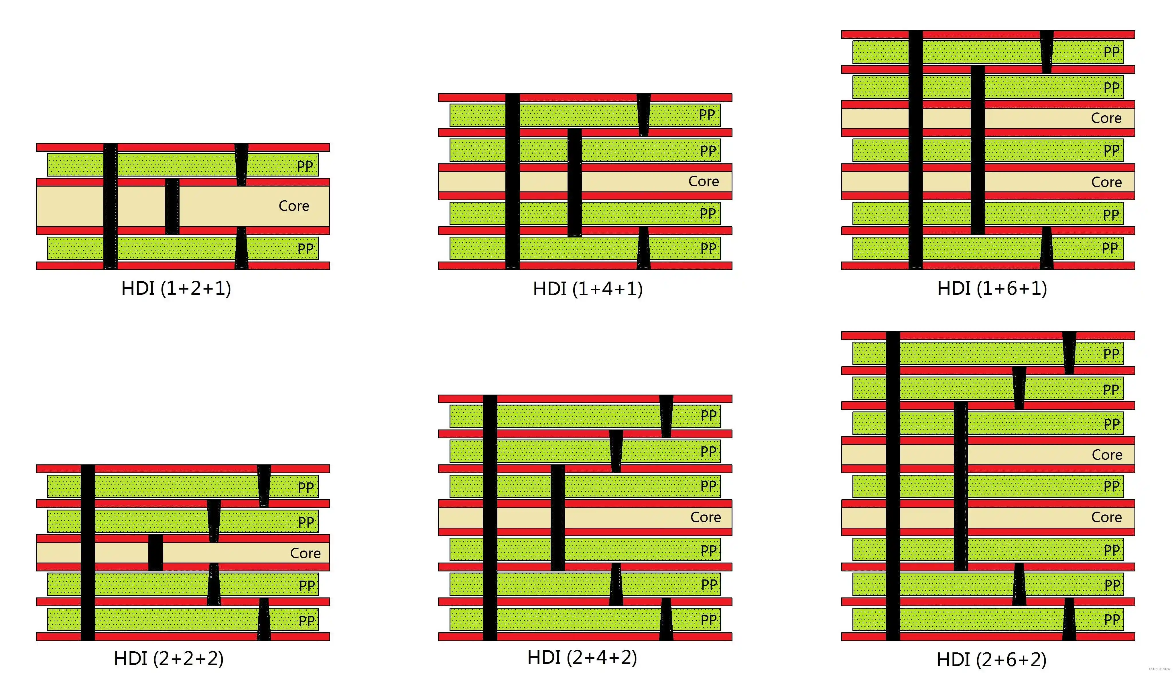
How many motherboard PCB layers are there?
The number of motherboard PCB layers varies widely based on application complexity. There is no fixed standard, but trends are clear across industries.
Entry-level embedded motherboards may use four layers. This configuration allows basic separation of power, ground, and signals. It suits moderate-speed designs with limited interfaces.
More advanced systems often use six to eight layers. These additional layers improve signal routing freedom and noise control. Industrial and communication products commonly fall into this range.
High-performance motherboards, such as those used in servers or advanced computing, may use ten layers or more. These designs support dense routing, multiple power domains, and high-speed buses.
At EBest Circuit (Best Technology), multilayer PCB capabilities support a wide range of motherboard PCB layer counts. Stack-ups are customized to balance cost, performance, and manufacturability.
Conclusion:
The comparison of circuit board vs motherboard becomes straightforward once roles are clearly defined. A circuit board is the foundation of electronic connectivity, while a motherboard is a specialized circuit board that coordinates an entire system. Every motherboard is a printed circuit board, but only a small portion of PCB boards qualify as motherboards.
Whether you are building a single-function PCB board or a full system motherboard, professional guidance makes a measurable difference.
For technical consultation, PCB fabrication, or PCBA services, you can contact the EBest Circuit (Best Technology) team directly at sales@bestpcbs.com