What is smoke detector PCB? Let’s discover its components, working principle, types, function, design guide and production processes for smoke detector PCB.
Are you worried about these problems?
- Why do traditional smoke detector PCBAs suffer from persistent high false alarm rates?
- How to resolve signal interference issues in multi-sensor collaborative systems?
- How to ensure product launch timelines when factories frequently delay deliveries?
EBest Circuit (Best Technology) can provide you solution and service:
- False Alarm Optimization: Differential signal processing + environmental self-learning algorithm reduces false alarms to <0.5%/1000h (UL268 certified).
- Signal Integrity Protection: System-level shielding design enables simultaneous operation of CO/photoelectric/pyroelectric sensors with >60dB crosstalk suppression.
- Agile Delivery System: Shenzhen-Vietnam dual production bases support 72h sample delivery + 15-day bulk shipment (includes burn-in test report).
Welcome to contact us if you have any request for Smoke Detector PCB design, prototyping, mass production, assembly: sales@bestpcbs.com.
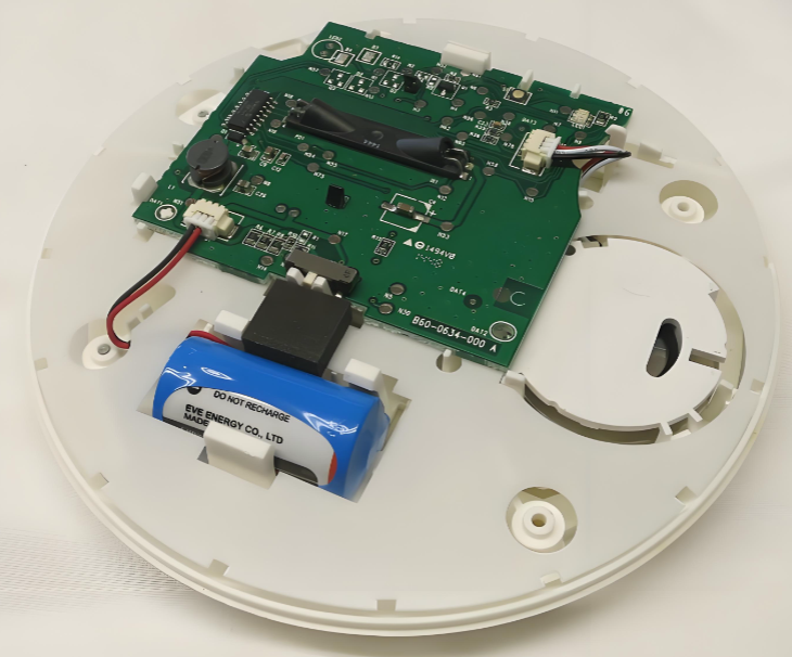
What Is Smoke Detector PCB?
The Smoke Detector PCB(also called as smoke detector circuit board) is the core component of smoke alarm devices. It integrates high-sensitivity smoke sensors, signal-processing microprocessors, and audible or visual alarm modules via precise circuit design. This enables real-time monitoring of smoke particle concentration changes.
When the detected value exceeds the safety threshold, it triggers local alarms and sends anomaly signals to the control system. With low-power design for extended battery life and electromagnetic interference resistance, it ensures stable operation in homes, offices, and industrial settings, providing reliable technical support for early fire warning.
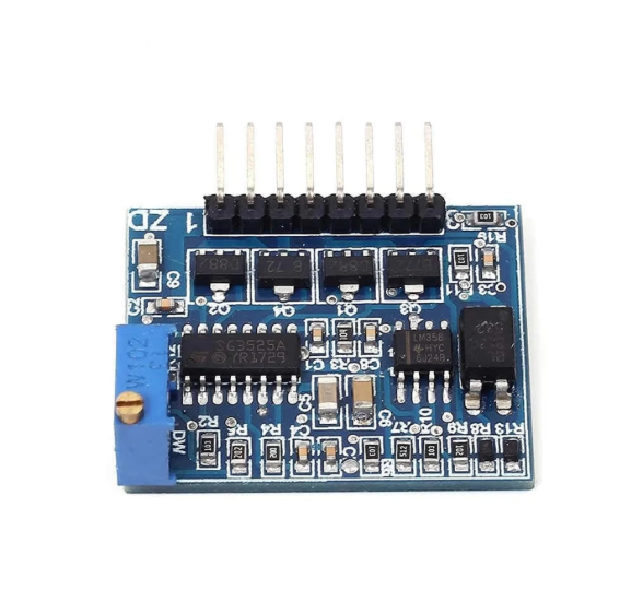
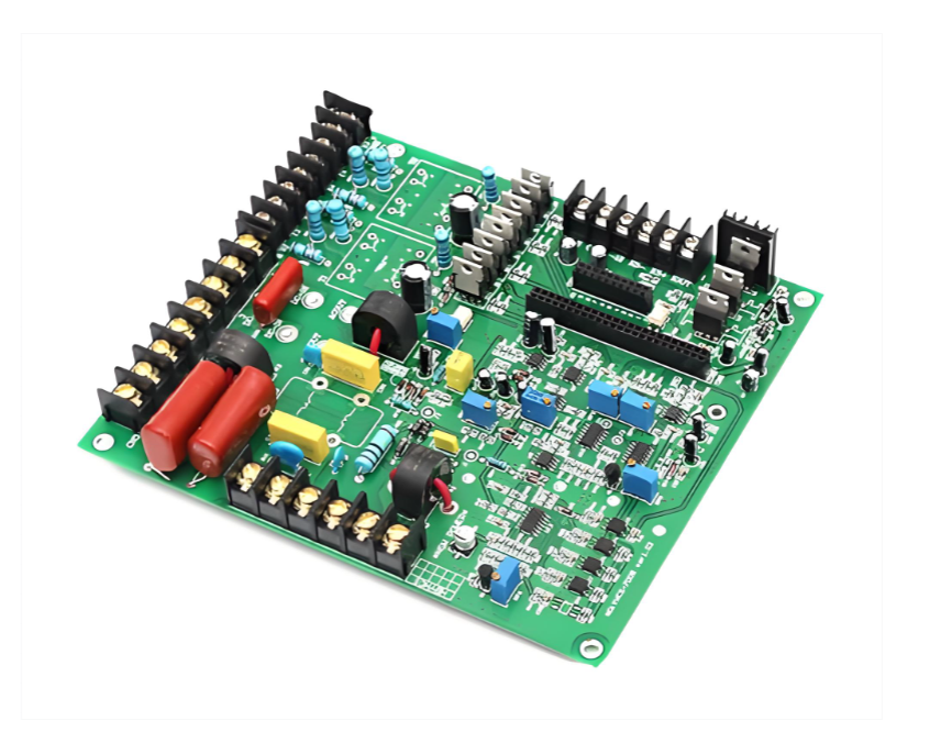
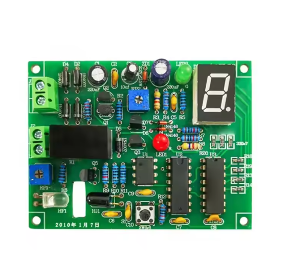
Smoke Detector PCB Components List
- Photoelectric Sensor Module: Contains infrared emitter and photodetector; detects smoke particles via light scattering effects, highly sensitive to smoldering smoke.
- Ionization Sensor Unit: Houses radioactive material (e.g., Americium-241) to create an ionization chamber; monitors disruptions in ion flow caused by smoke particles, responsive to fast-flaming fire particles.
- Main Microcontroller: Processes signals, judges thresholds, controls logic, and triggers alarm circuits; integrates low-power design for extended battery life.
- Audible-Visual Alarm Module: Combines a buzzer (≥85dB output) and LED indicators; activates simultaneous sound/light alerts upon detection, with multi-color LEDs for status differentiation.
- Power Management System: Integrates battery/AC interfaces, voltage regulators (e.g., 7805), and low-power management; supports dual-power supply (battery/mains) for uninterrupted operation during outages.
- Signal Conditioning Circuit: Comprises preamplifiers, filters, and comparators; amplifies, filters, and compares weak sensor signals to enhance stability and anti-interference performance.
- Communication Interface Module: Optional Wi-Fi/Bluetooth modules or wired interfaces; enables networked alerts and status sync with smart home systems or central control panels.
- Test & Status Indication Unit: Features manual test buttons, power LEDs, and self-diagnostic circuits; allows user testing and visual monitoring of device health.
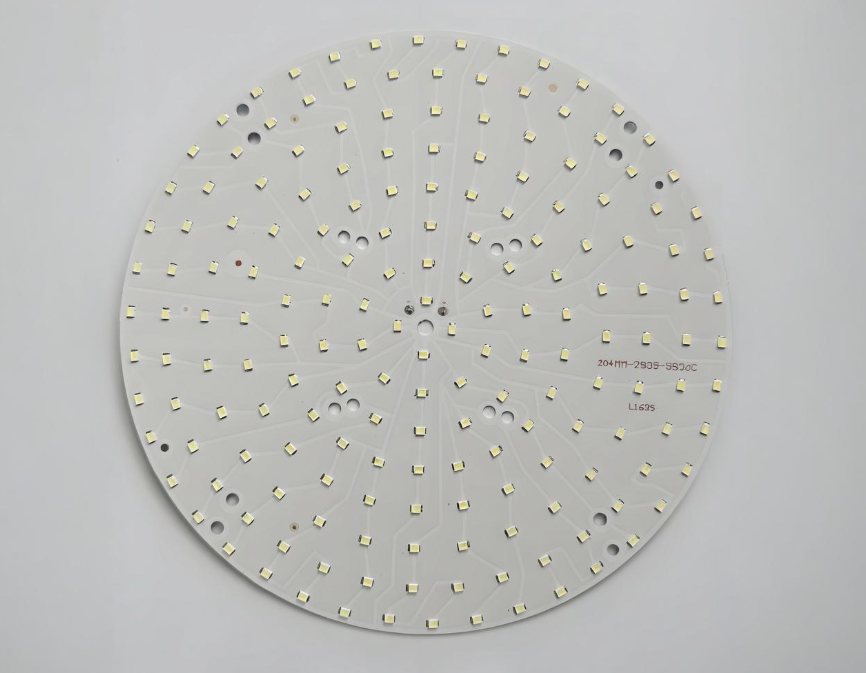
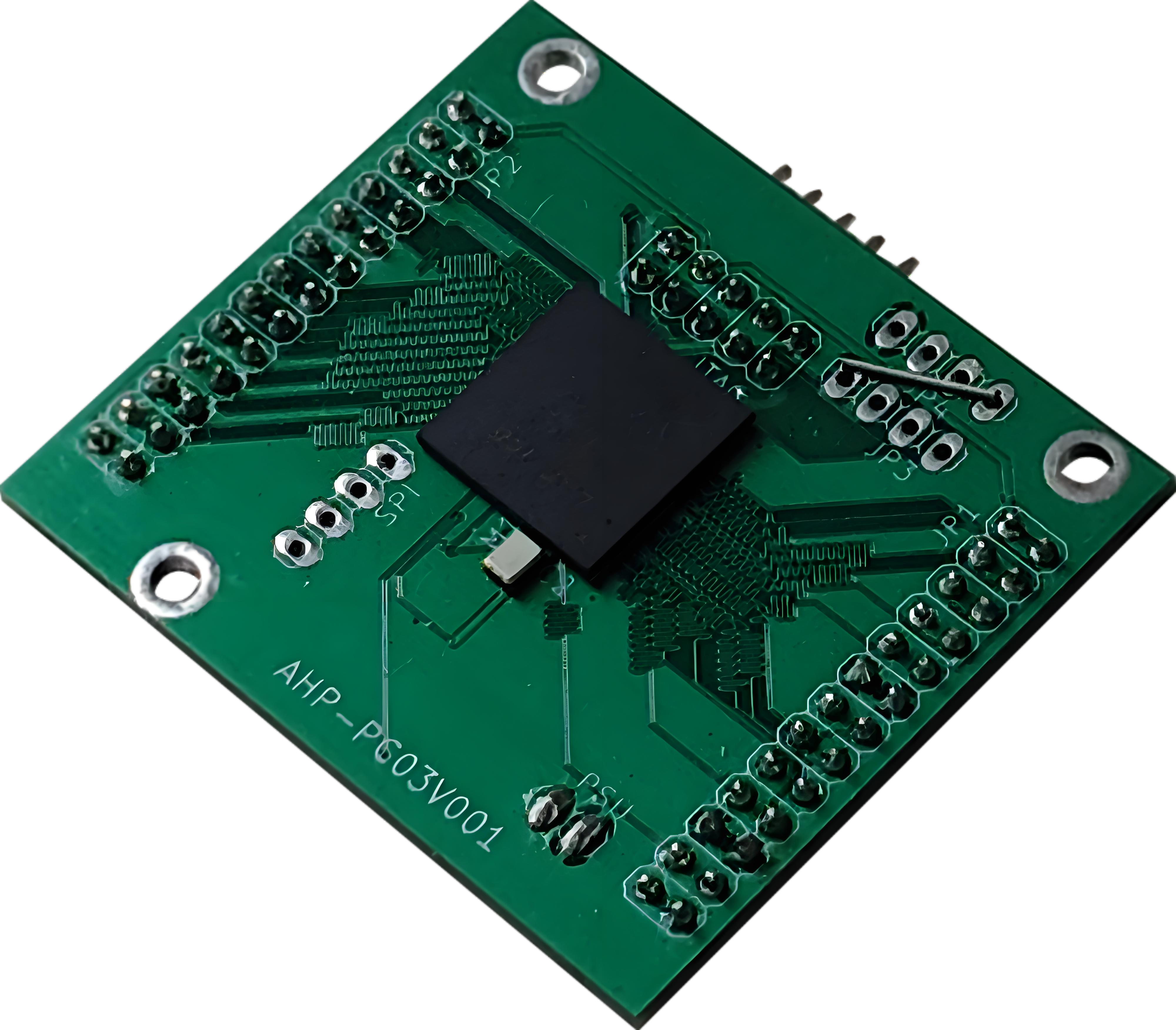
- PCB Substrate & Passive Components: Built on FR4 substrate with resistors, capacitors, inductors; ensures signal integrity, EMC compliance, and thermal efficiency via precision routing.
- Smoke Chamber Structure: Optimized cavity design for efficient smoke entry and detection; enhances sensitivity and response speed for light-scattering/ionization detection.
Smoke Detector PCB Working Principle
1. Dual Smoke Detection Modes: Uses both photoelectric sensors (detecting smoldering smoke via light scattering) and ionization sensors (tracking fast-flaming fire particles through Americium-241-powered ion flow disruption) for wider coverage.
2. Signal Cleanup & Enhancement: Weak signals from sensors are amplified, filtered to remove dust/temperature noise, and compared against safety thresholds to ensure only real smoke triggers alerts.
3. Smart Decision-Making: The main chip analyzes signals alongside temperature/humidity data to avoid false alarms (e.g., from steam or dust) and fine-tunes sensitivity using built-in algorithms.
4. Clear Multi-Stage Alerts: When smoke is detected, a loud buzzer (≥85dB) sounds and LEDs flash red. Advanced models add voice alerts or phone notifications via apps.
5. Always-On Power Backup: Runs on mains electricity but switches to backup batteries during outages. Low-power design keeps it working for 10+ years, with battery warnings before failure.
6. Connected Safety Network: Built-in Wi-Fi/Bluetooth or wired connections send alerts to smart home systems, fire departments, or property managers for instant response.
7. Self-Checking Health Monitor: Daily automatic checks verify sensor accuracy, circuit health, and battery status. LEDs or apps show device condition, ensuring it’s always ready to protect.
Types of Smoke Detector Circuit Board
- Photoelectric Smoke Detector Circuit Board: Uses infrared LED and photodiode to detect smoke via light scattering, sensitive to larger smoke particles from smoldering fires (like homes, offices).
- Ionization Smoke Detector Circuit Board: Relies on radioactive material to ionize air; smoke particles disrupt ion flow to trigger alarms, ideal for fast-flaming fires, such as industrial sites.
- Gas-Sensitive Smoke Detector Circuit Board: Detects specific gases (like CO, methane) through semiconductor resistance changes, used for gas leaks in kitchens or chemical plants.
Functions of Smoke Detector Circuit Board
Smoke Detection & Signal Acquisition
- Integrates photoelectric, ionization, or gas-sensitive sensors to detect smoke particles/gas molecules via infrared scattering, ion current changes, or gas-sensitive resistance, enabling precise environmental monitoring.
Signal Processing & Amplification
- Processes weak sensor signals through transimpedance amplification, low-pass filtering, and ADC digitization. Enhances signal-to-noise ratio and supports calibration algorithms for accurate concentration measurement.
Threshold Judgment & Alarm Activation
- Real-time monitoring by MCU/comparator triggers local audible-visual alarms (buzzer + LED) and remote alerts (Wi-Fi/Zigbee/CAN bus) when smoke levels exceed preset thresholds.
Power Management & Safety Protection
- Uses LDO voltage regulators for stable power supply (e.g., 5V/3.3V). Integrates low-battery detection, overcurrent protection, reverse-polarity protection, and power isolation to ensure safe operation.
Self-Check & System Integration
- Supports periodic self-tests (simulated smoke testing), fault code indication (e.g., sensor failure/communication errors), and device linkage (fire sprinklers/ventilation/relay control) for end-to-end intelligent management.
How to Design a Photoelectric Smoke Detector PCB?
1. Requirement Analysis & Scenario Adaptation
- Functional Requirements: Define core functions (smoke scattering detection, audible-visual alarm, remote communication) and auxiliary functions (low-battery alert, self-diagnosis).
- Technical Parameters: Set operating voltage (DC 9-24V), smoke detection range (0-5000PPM), response time (≤1 second), communication protocols (I²C/RS485), and protection grade (IP42).
- Scenario-Specific Thresholds: For residential use, set smoke threshold ≤500PPM to avoid false alarms from cooking fumes; for industrial use, lower to ≤300PPM for higher sensitivity; commercial scenarios optimize for integrated control needs.
2. Sensor & Core Component Selection
- Sensor Selection: Use NIS-09C photoelectric sensor (880nm IR LED + photodiode) for high-sensitivity smoke scattering detection.
- Driver Circuit: Adopt LM317 constant-current driver to stabilize IR LED emission intensity, preventing brightness fluctuations that affect detection accuracy.
- MCU Selection: Choose STM32 series microcontroller with integrated ADC for signal digitization and low-power operation support.
- Power Management: Implement TPS5430 + AMS1117-3.3 cascaded design; use MAX809 power monitoring chip for low-battery detection (6.5V threshold alarm).
3. Schematic Architecture Design
- Sensor Interface: IR LED driver (PWM dimming control) + photodiode signal acquisition (OPA333 transimpedance amplifier + 10Hz cutoff 2nd-order LPF).
- Signal Processing: Connect sensor signals to MCU ADC channels; apply moving average filtering for concentration calibration and dynamic baseline calibration algorithms for temperature/humidity adaptation.
- Communication Interface: Integrate RS485 transceiver (Modbus-RTU support) or wireless modules (e.g., ESP32); add SMAJ15A TVS diodes for surge protection and 6N137 optocouplers for galvanic isolation.
- Alarm & Self-Test Circuits: Audible-visual alarm (buzzer + LED driver), simulated smoke test interface (button-triggered), and sensor contamination detection (baseline drift monitoring).
4. PCB Layout & Signal Integrity Optimization
- Stack-Up Design: 4-layer PCB with “signal-ground-power-signal” stack-up to minimize EMI.
- Critical Routing: High-speed signals (MCU clocks, communication buses) use differential pairs with ≥8mil width/10mil spacing; analog signals employ ground shielding to prevent digital crosstalk.
- Power Integrity: Add π-type filter (common-mode choke + X/Y capacitors) at power entry; place copper pour under LDO chips for heat dissipation; add decoupling capacitors (100nF+10μF) near critical circuits.
- Thermal & Material Selection: Use 1206 resistors with heatsinks; for industrial-grade applications, select high-Tg PCB material (Tg≥170°C) to resist thermal deformation; validate thermal design via simulation.
5. Anti-Interference & Long-Term Reliability Design
- Environmental Noise Mitigation: Implement ground shielding for analog paths and serpentine traces for digital signal impedance matching; suppress high-frequency noise with π-type filtering at power inputs.
- Reliability Verification: Conduct accelerated life testing (1000h at 85°C/85%RH) to validate component stability; perform periodic simulated contamination tests (dust coverage detection) to ensure self-cleaning activation.
- Fault Diagnosis: Auto-calibrate ambient light interference via baseline tracking circuits; display fault codes through LED blinking patterns and support remote fault reporting.
6. Testing & Fault Diagnosis
- Lab Testing: Use CRC-90-009 smoke generator to simulate concentrations; verify ADC sampling error ≤2% with digital oscilloscopes; test power management stability under voltage fluctuations using programmable supplies.
- Field Testing: Record false/missed alarm rates over 72h real-world operation (kitchens/warehouses); industrial models must pass CE/FCC EMC certification for stable performance in complex electromagnetic environments.
- Fault Injection: Test response speed (≤1s alarm trigger) and accuracy under induced faults (sensor contamination, power shorts).
7. Documentation & Mass Production Optimization
- Design Package: Include schematics (PDF + Altium source), Gerber files, BOM (part numbers/footprints/suppliers), and test specifications.
- Production Control: Adopt lead-free processes (RoHS compliant); perform 100% AOI inspection for critical components; conduct thermal shock testing (-40°C~120°C, 3 cycles) and vibration testing (10G rms random vibration).
- Cost & Manufacturing Optimization: Reduce BOM costs through component optimization (e.g., STM32 series MCUs); improve SMT efficiency via panelization (V-cut); adhere to 3W rule for acid trap avoidance; place test points at board edges for ICT accessibility.
How to Make a Photoelectric Smoke Detector PCB?
Photoelectric Smoke Detector PCB Manufacturing Process
1. Material Cutting & Substrate Preparation: Select UL217-compliant FR4 double-sided copper-clad substrate, cut into 38mm×38mm unit boards. Surface cleanliness must meet IPC-6012 Class 2 standards (no oxidation/oil residue) to ensure reliable foundation for precision processing.
2. Drilling & Through-Hole Plating: Use CNC drilling to create component pin holes, vias, and test points with ±0.05mm accuracy. Apply chemical copper deposition and electroplating to form conductive pathways, ensuring hole wall copper thickness ≥25μm for reliable electrical connections between photoelectric sensor modules and microcontrollers.
3. Etching & Circuit Formation: Transfer circuit patterns via dry film photolithography, followed by acid etching to remove excess copper, forming high-precision traces (line width/spacing ≥0.1mm). Optimize scatter path layout for photoelectric sensors (infrared LED + photodetector) to ensure alignment accuracy ≤0.1mm, enhancing sensitivity to smoldering smoke.
4. Solder Mask & Surface Finish: Apply green photosensitive solder mask ink, exposed and developed to form protective layers preventing short circuits. Use ENIG (Electroless Nickel Immersion Gold) surface treatment with ≥3μin thickness to ensure reliable soldering and long-term corrosion resistance for microcontrollers and communication modules (Wi-Fi/Bluetooth).
5. SMT Placement & Reflow Soldering: Automatically place surface-mount components (photoelectric sensors, microcontrollers like RE46C190, low-power capacitors/resistors) via SMT machine. Solidify connections through a 10-zone reflow oven, ensuring AOI-verified solder joints with no defects (e.g., cold solder, bridges).
6. THT Insertion & Wave Soldering: Manually insert through-hole components (buzzer, power connector, test buttons) and wave-solder to ensure mechanical strength ≥30N. Validate solder quality via X-ray inspection to eliminate hidden defects.
7. Functional Testing & Calibration: Verify circuit continuity and impedance via ICT; simulate smoldering smoke using a smoke generator to test response time (≤10s) and alarm threshold (≥3% obscuration). Calibrate audible-visual alarm (≥85dB buzzer, LED flash frequency) to meet GB4715-2005 standards.
8. PCBA Assembly & Housing Integration: Assemble PCB with housing, power module (AC/battery dual supply), and communication interfaces (485 bus/Wi-Fi). Implement self-diagnostic functions (daily sensor/battery health checks) with status feedback via LED/APP.
9. Environmental & Certification Testing: Conduct thermal cycling (-10°C~60°C), constant humidity (95%RH) tests, and EMC/anti-interference validation. Pass UL217/UL268 certification (including false alarm rate checks) to ensure global safety compliance.
10. Final Packaging & Labeling: Use anti-static bags + carton packaging, labeled with UL certification marks, production batch, and installation guides. Include mounting bases and user manuals for plug-and-play deployment in residential/commercial/industrial settings.
Why Choose EBest Circuit (Best Technology) as Smoke Detector PCB Assembly Manufacturer?
Reasons why choose us as smoke detector PCB assembly manufacturer:
- Cost-Effective Pricing Structure: Optimized production flow reduces per-unit cost by 15-20% through material bulk procurement and process automation. Transparent pricing model with no hidden fees, ensuring budget predictability for large-scale orders.
- Ultra-Fast Lead Time: 7-day rapid prototyping to volume production transition, with 99.2% on-time delivery rate. Supports 3-day expedited service for critical projects, backed by real-time production tracking systems.
- Full-Suite PCBA Services: End-to-end solutions from DFM consultation to final testing, including SMT, through-hole assembly, and conformal coating. Customizable service packages accommodate NPI (New Product Introduction) to mass production needs, with design-for-manufacturing (DFM) support to minimize yield loss.
- High-Reliability Quality Assurance: ISO quality standards with IPC-A-610 Class 2/3 compliance. Products pass 100+ rigorous tests including thermal cycling (-40°C~125°C), vibration resistance (10G rms), and 1000-hour accelerated life testing (85°C/85%RH).
- Multi-Layered Quality Control: 12-step inspection process including AOI (Automated Optical Inspection), X-ray for BGA/solder joint integrity, and in-circuit testing (ICT). Statistical Process Control (SPC) monitors critical parameters in real-time, achieving <0.1% defect rate.
- Advanced Technical Support: Dedicated engineering team provides 24/7 DFM feedback, signal integrity analysis, and thermal simulation. On-site technical troubleshooting during prototyping stages to preempt manufacturing issues.
Our PCBA Capabilities
| Item | Capabilities |
| Placer Speed | 13,200,000 chips/day |
| Bare Board Size | 0.2 x 0.2 inches – 20 x 20 inches/ 22*47.5 inches |
| Minimum SMD Component | 01005 |
| Minimum BGA Pitch | 0.25mm |
| Maximum Components | 50*150mm |
| Assembly Type | SMT, THT, Mixed assembly |
| Component Package | Reels, Cut Tape, Tube, Tray, Loose Parts |
| Lead Time | 1 – 5 days |
How to Get a Quote for Your Smoke Detector PCB Project?
1. Design File Package
- Gerber files (including stack-up structure, impedance control requirements)
- BOM (Bill of Materials) with part numbers, footprints, quantities, and preferred suppliers
- PCB design files (Altium/PADS source or PDF)
2. Specifications
- Board parameters: Layer count (e.g., 4-layer), dimensions (e.g., 100×100mm), substrate type (FR4/CEM3), copper thickness (1oz/2oz), surface finish (HASL/ENIG/OSP)
- Advanced processes: Blind/buried vias, back drilling, impedance control (e.g., 50Ω±10%), ENIG thickness (e.g., 2μm)
3. Quantity & Lead Time
- Order type: Prototype (5-100 units), small batch (100-5000 units), mass production (5000+ units).
- Lead time: Standard (15-20 business days), expedited (3-7 business days).
4. Quality & Certification Requirements
- Inspection standards: IPC-A-610 Class 2/3, AOI/X-ray inspection, flying probe testing
- Certifications: UL, CE/FCC compliance, RoHS lead-free process
- Reliability tests: 85°C/85%RH 1000h accelerated aging, thermal shock (-40°C~125°C, 3 cycles)
5. Additional Service Needs
- Assembly options: SMT+DIP hybrid assembly, selective wave soldering
- Packaging: ESD-safe packaging, vacuum sealing, humidity indicator cards
- Special requirements: Custom labeling, laser marking, batch traceability codes
Welcome to contact us if you have any request for smoke detector circuit boards: sales@bestpcbs.com.