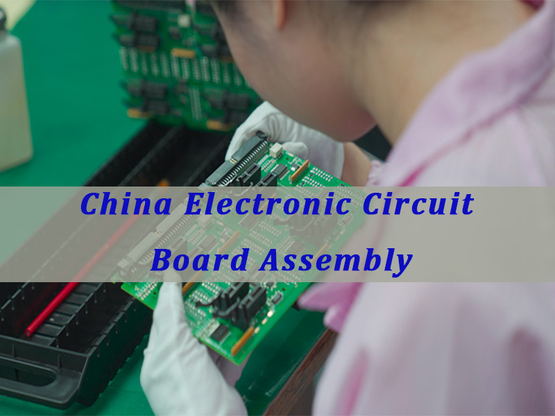
Are you tired of inconsistent quality, delayed shipments, and limited technical support when sourcing PCB assembly and manufacturing services in Syria? Many regional buyers face consistent roadblocks when trying to secure durable, compliant, and timely PCB assembly and manufacturing services in Syria, with no reliable partner to handle complex prototypes, high-volume runs, or specialized industry boards. This guide breaks down critical regional challenges, end-to-end service solutions, and why EBest stands as the most trusted global partner for Syria-based PCB orders.
Common Challenges of PCB Assembly and Manufacturing Services in Syria
- Unstable Electronic Component Supply Chains: Local and regional suppliers often face stock shortages, long lead times for specialized components (including BGA, QFN, and high-precision parts), and limited access to authentic, RoHS/REACH-compliant components, leading to production delays and non-compliant finished boards.
- Limited Advanced Assembly Capabilities: Most local providers lack equipment for high-density assembly, fine-pitch BGA soldering, flexible PCB assembly, and ceramic PCB manufacturing, making it impossible to fulfill medical, aerospace, and industrial device orders that require strict precision and compliance.
- Complex Cross-Border Logistics & Customs Delays: International shipping and customs clearance for PCB materials and finished assemblies are often slow and unregulated, with poor protective packaging leading to ESD damage, moisture contamination, or physical breakage of sensitive PCBs.
- Inconsistent Quality Control & Missing Industry Certifications: Few regional manufacturers hold IATF 16949, ISO 13485, AS9100D, or UL certifications, and lack standardized testing protocols (AOI, ICT, FCT), resulting in high defect rates and failed compliance checks for critical industry applications.
- Slow Turnaround for Prototypes & Urgent Orders: Quick-turn PCB assembly and low-volume prototype production are rarely offered locally, forcing buyers to wait weeks for sample boards and miss tight product development deadlines.
End-to-End PCBA Services from Requirements to Delivery
EBest eliminates every key challenge of PCB assembly in Syria with a fully integrated, turnkey workflow that covers every stage from initial design review to final doorstep delivery, with zero gaps in support or quality. We tailor this full-cycle process to match Syria order requirements, regulatory needs, and regional logistics constraints. Here are our tailored solutions to the above challenges:
- Design Review & DFM Optimization: Our engineering team conducts free Design for Manufacturing (DFM) checks before production starts, fixing layout flaws, component placement issues, and material selection gaps to avoid costly reworks. This directly solves the problem of poor design compatibility with limited local assembly capabilities.
- Global Component Sourcing & Stock Management: We maintain a stable, global supply chain for all electronic components (SMD, BGA, QFN, QFP, and specialty parts) with full traceability and compliance. We source only certified components, eliminating stock shortages and counterfeit part risks that plague local Syria PCB procurement.
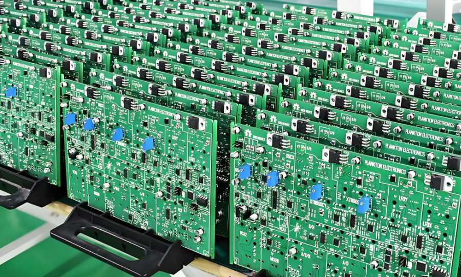
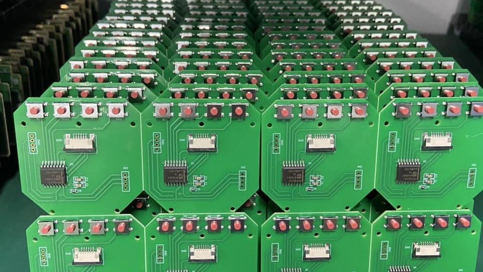
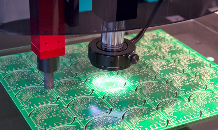
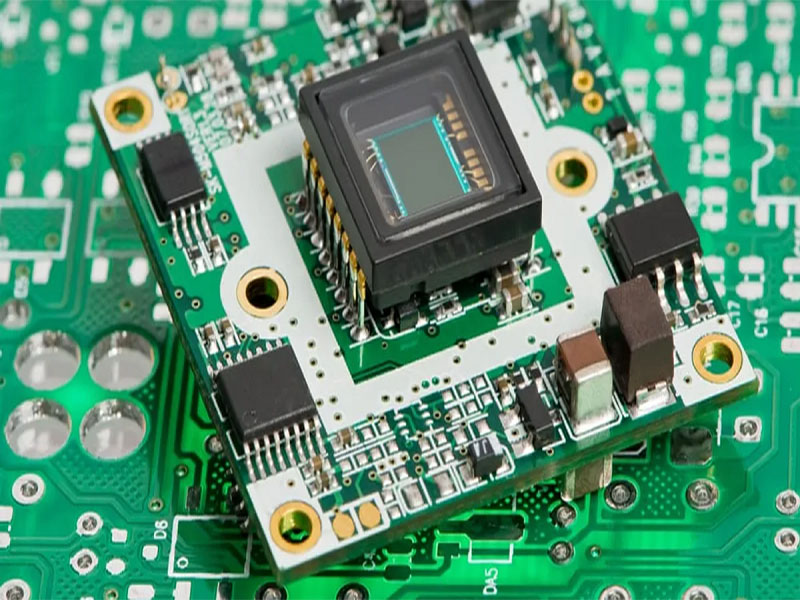
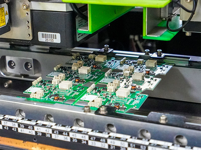
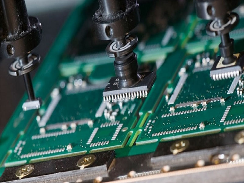
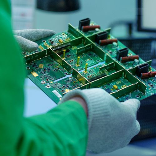
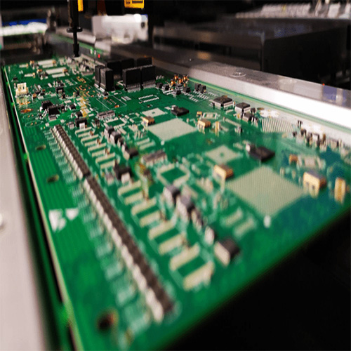
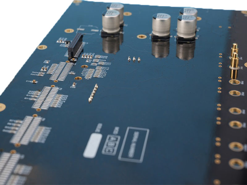
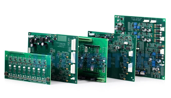
- Advanced PCB Fabrication & Assembly: Our 19+ year manufacturing facility handles all PCB types (FR4, multi-layer, ceramic, flex, rigid-flex, high-frequency) and assembly types (SMT, THT, mixed, BGA). We use fully automated production lines to deliver precision that local providers cannot match, supporting medical, aerospace, and industrial grade orders.
- Strict Quality Testing & Compliance Verification: We perform 100% full inspection and multi-stage testing (AOI, X-ray for BGA, ICT, FCT) to meet global certification standards (IATF 16949, ISO 9001, ISO 13485, AS9100D, RoHS, REACH, UL). This ensures every PCB assembly for Syria meets industry-specific quality and regulatory rules.
- Secure Logistics & Expedited Shipping: We use ESD-safe, moisture-resistant packaging and partner with reliable cross-border logistics providers to streamline customs clearance. We offer expedited shipping options, ensuring secure and on-time delivery even for urgent Syria orders, solving regional logistics delays.
Why Choose EBest for PCB Assembly and Manufacturing Company in Syria?
Here are reasons why choose EBest for PCB assembly and manufacturing services in Syria:
- 19+ Years of Specialized PCB & PCBA Expertise: As a veteran global manufacturer with nearly two decades of focused experience, we routinely handle complex, high-precision international orders for medical, aerospace, and industrial electronics. This deep industry expertise is unmatched by local PCB providers in Syria, allowing us to solve even the most demanding assembly and manufacturing challenges.
- Full Industry Certification Compliance: We hold strict global certifications including IATF 16949 (automotive), ISO 9001:2015 (quality), ISO 13485:2016 (medical), AS9100D (aerospace), RoHS, REACH, and UL. Every PCB assembly and manufacturing order for Syria adheres to these rigorous standards, ensuring full regulatory compliance for critical industry applications.
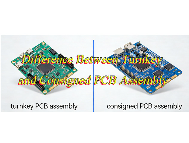
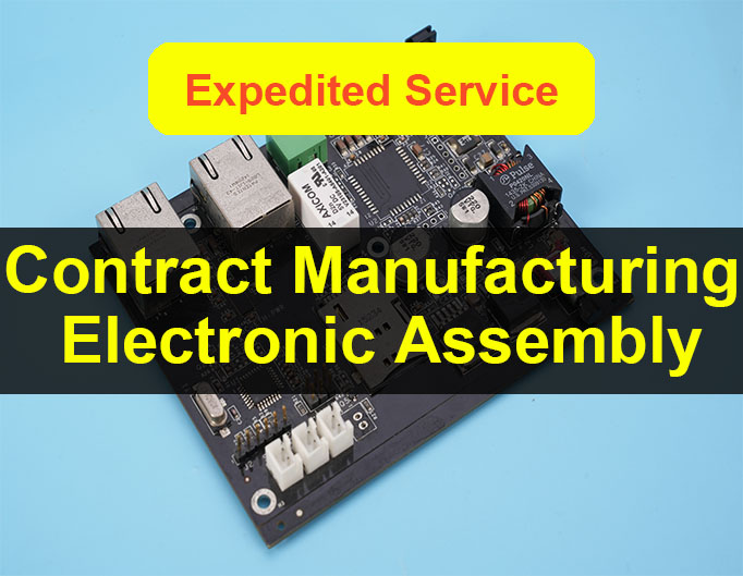
- Complete Turnkey & Quick-Turn Solutions: We offer full turnkey PCB assembly services in Syria, plus rapid prototype production and 24-hour expedited assembly for urgent orders. This eliminates the long lead times that plague local sourcing, and we maintain strict quality standards even for accelerated production timelines.
- Stable Global Component Supply Chain: Our dedicated procurement team manages a vetted, global component network with zero counterfeit component risks. We guarantee consistent stock for standard and specialty components (SMD, BGA, QFN, QFP) required for Syria-based PCB projects, avoiding production delays from supply shortages.
- Advanced In-House Manufacturing Capabilities: We operate fully automated assembly lines, precision fine-pitch BGA soldering equipment, and dedicated production for flex, ceramic, and high-frequency PCBs. These capabilities let us support high-complexity orders that local Syrian manufacturers cannot accommodate, with tight tolerances and consistent quality.
- 100% Full Inspection & Quality Guarantee: Every finished PCB assembly undergoes rigorous multi-stage testing and full pre-shipment inspection, resulting in industry-leading low defect rates for all Syria orders. We provide full quality documentation to validate compliance and performance for every batch.
- Full-Lifecycle Traceability via MES System: Our dedicated MES (Manufacturing Execution System) enables complete end-to-end traceability for all Syria PCB orders. It tracks component batches, production steps, test results, and inspection data in real time, supporting full auditability, fast compliance checks, and full transparency from raw materials to final delivery—an exclusive advantage over local Syrian PCB suppliers.
What Types of PCB Assembly and Manufacturing Services in Syria Does EBest Offer?
Here are types of PCB assembly and manufacturing services in Syria we offer:
- Standard & Multi-Layer PCB Fabrication: FR4, metal-core (MCPCB), and high-frequency PCB production for general electronics and industrial equipment, with customizable layer counts and substrate materials.
- Specialized PCB Assembly: BGA Assembly, Through-Hole (THT) Assembly, Flex PCB Assembly, Ceramic PCB Assembly for high-temperature and high-reliability applications.
- Prototype & Low-Volume PCB Production: Quick-turn prototype assembly and small-batch production for product development and testing, ideal for startups and engineering projects in Syria.
- Full Turnkey PCB Assembly: End-to-end service covering component sourcing, PCB fabrication, assembly, testing, and shipping—one partner for the entire project, no middlemen.
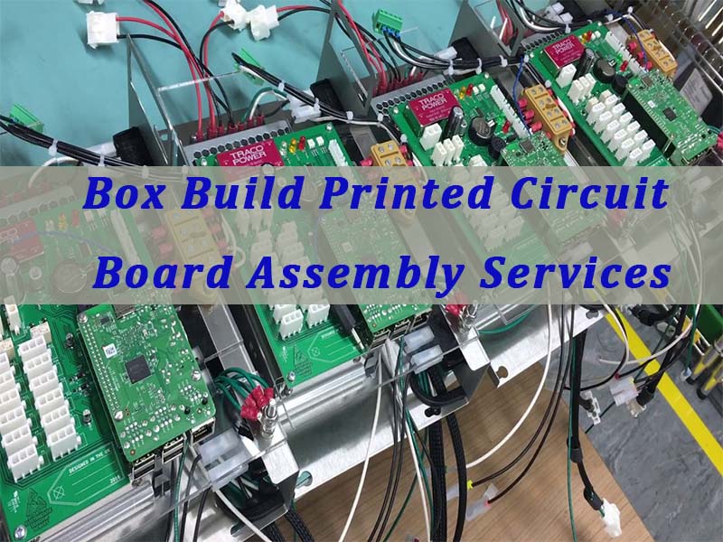
- Box Assembly & Value-Added Services: Complete box build assembly, injection molding, CNC machining, and sheet metal fabrication for finished electronic devices, beyond basic PCB assembly.
- High-Volume & Mass Production PCB Assembly: Scalable production for industrial, automotive, and commercial electronics, with consistent quality across large order volumes for Syria-based buyers.
How Does EBest Ensure High-Quality PCB Assembly in Syria?
Methods about we ensure high quality PCB assembly in Syria:
- Strict Component Qualification & Testing: All incoming components are tested for authenticity and compliance; we reject non-certified or counterfeit parts before they enter production, eliminating quality risks at the source.
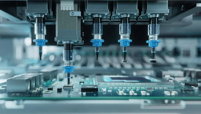
- Automated Precision Assembly Equipment: High-speed placement machines (13.2 million chips/day capacity) and controlled soldering processes ensure consistent, accurate component placement, even for 01005 micro SMD parts and 0.25mm fine-pitch BGA.
- Multi-Stage Quality Testing Protocol: In-line AOI (Automated Optical Inspection), X-ray inspection for hidden BGA solder joints, ICT (In-Circuit Test), and FCT (Functional Test) to catch defects early and ensure full electrical functionality.
- Adherence to IPC & Global Industry Standards: All assembly processes follow strict IPC-A-610 standards, paired with our certified quality management systems to maintain uniform quality across every Syria order.
- Controlled Production Environment: ESD-protected, temperature and humidity-controlled manufacturing floors prevent electrostatic damage and moisture-related defects, critical for sensitive PCB assemblies.
- Final Pre-Shipment Full Inspection: Every finished PCB assembly undergoes a final full inspection before shipping to Syria, with detailed quality reports provided for full transparency.

How We Ensure On-Time Delivery of Syria PCB Assembly Orders?
Methods about how we ensure on-time delivery of Syria PCB assembly orders:
- Transparent Order Scheduling & Real-Time Updates: We provide fixed lead times (1-5 days for standard orders) and real-time production tracking, so you always know your order status with no unexpected delays.
- Optimized Production Workflow: Streamlined, automated production lines reduce processing time; we prioritize urgent Syria orders for quick-turn assembly without sacrificing quality.
- Global Component Stock Buffer: We maintain safety stock for high-demand components, eliminating production halts caused by component shortages common in regional Syria supply chains.
- Experienced Cross-Border Logistics Management: Pre-approved logistics partners and streamlined customs documentation reduce border delays; we use expedited shipping for time-sensitive orders to meet tight deadlines.
- ESD & Damage-Proof Packaging: Industrial-grade protective packaging prevents shipping damage, avoiding costly returns and re-delivery delays for Syria-bound orders.
- Proactive Order Monitoring: Our logistics team monitors every shipment end-to-end, resolving potential delays before they impact delivery to your Syria location.
EBest’s PCB Assembly Capabilities for Syria Orders
| Technical Specification | Value/Description |
| Placement Speed | 13,200,000 chips per day |
| Bare Board Size Range | 0.2 x 0.2 inches to 22 x 47.5 inches |
| Minimum SMD Component Size | 01005 (micro-miniature components) |
| Minimum BGA Pitch | 0.25mm (fine-pitch high-precision assembly) |
| Max Component Mounting Area | 50 x 150mm |
| Assembly Types Supported | SMT, THT, Mixed SMT-THT Assembly |
| Component Package Compatibility | Reels, Cut Tape, Tube, Tray, Loose Parts |
| Standard Lead Time | 1-5 business days |
| Expedited Service | 24-hour rush shipping available for urgent orders |
| Monthly Production Capacity | 260,000 square feet (28,900 square meters), 1000+ unique board designs |
Case Studies of Our Syria PCB Assembly and Manufacturing Project
Project Background
A Syria-based medical device company needed PCB assembly and manufacturing services in Syria for a critical patient monitoring device PCB, requiring ISO 13485 medical certification, zero-defect quality, and strict compliance with healthcare industry standards. The client previously worked with a local provider that failed compliance checks and delivered inconsistent, defective boards.
Project Requirements
This project called for a high-reliability 4-layer rigid-flex medical PCB assembly tailored for a patient monitoring device, with non-negotiable quality and compliance mandates. Core requirements included strict adherence to ISO 13485 medical device standards and RoHS compliance, fine-pitch BGA component assembly for compact device design, 100% full functional testing to guarantee patient safety, and complete traceability for all materials and production steps to meet healthcare regulatory audit rules. The client also required formal quality certification documentation for every finished board to validate compliance and performance.
Project Challenges
The client faced major roadblocks with local PCB assembly and manufacturing services in Syria before partnering with EBest. Primary challenges included an extremely tight 5-day lead time for prototype-to-small-batch production, limited access to certified medical-grade electronic components via regional supply chains, zero defect tolerance for critical patient monitoring equipment, and lack of local providers capable of fine-pitch BGA soldering or meeting ISO 13485 medical certification standards. Cross-border shipping risks and lack of full production traceability from local suppliers further threatened project timelines and compliance.
Our Tailored Solution
EBest deployed a dedicated medical-grade PCB assembly workflow aligned with ISO 13485 standards, paired with our MES traceability system to track every component batch, production step, and test result end-to-end. Our engineering team completed free DFM optimization to refine board design for precision assembly, sourced fully certified medical-grade components through our global compliant supply chain, and used automated assembly lines paired with X-ray and AOI inspection to eliminate defects. We prioritized the order in our production schedule to meet the tight deadline, while maintaining strict quality controls and generating full compliance documentation for audit readiness.
Quantifiable Results
We delivered 250 finished medical PCBs in 4 days, 1 full day ahead of the agreed 5-day timeline with a flawless 0% defect rate across the entire batch. All units passed ISO 13485 and RoHS compliance audits on the first submission, and we provided complete MES-backed traceability reports and quality certification documents. The client has since named EBest their exclusive global partner for all medical and industrial PCB assembly in Syria, with 12+ consecutive repeat orders and zero quality or delivery issues to date.
FAQs About PCB Assembly and Manufacturing Services in Syria
Q1: What is the typical lead time for PCB assembly orders shipped to Syria?
A1: Standard lead time for PCB assembly services in Syria is 1-5 business days for most prototype and medium-volume orders. Expedited 24-hour rush service is available for ultra-urgent orders, with cross-border shipping time added based on your exact location in Syria. We lock in lead times upfront with no hidden delays.
Q2: Can you handle high-precision BGA and fine-pitch PCB assembly for Syria orders?
A2: Yes, EBest specializes in fine-pitch BGA assembly down to 0.25mm pitch and micro SMD 01005 component placement, fully supported by our advanced automated equipment and X-ray inspection. We regularly complete high-precision assemblies for aerospace, medical, and industrial devices bound for Syria.
Q3: Do you provide compliant components and certified PCB assembly for medical and aerospace use in Syria?
A3: Absolutely. We hold ISO 13485 (medical), AS9100D (aerospace), and IATF 16949 certifications, and source only fully compliant, traceable components. All medical and aerospace PCB assemblies for Syria meet strict industry standards and include full certification documentation.
Q4: How do you protect PCB assemblies from damage during shipping to Syria?
A4: We use ESD-safe, anti-static, moisture-barrier packaging designed for sensitive electronic assemblies, with shock-absorbent materials to prevent physical damage during cross-border transit. Every shipment is labeled and packed to meet international shipping standards, minimizing damage risk to near zero.
Q5: Can you support both small prototype runs and large-volume mass production for Syria clients?
A5: Yes, we accommodate full order scales from low-volume prototype PCB assembly (for product testing and development) to high-volume mass production. Our flexible production lines and global component supply chain let us scale seamlessly while maintaining consistent quality for all Syria orders, regardless of size.