Have you ever watched Marvel’s The Avengers? It is a movie telling a story that several superheroes get together to fight the bad guy Loki Laufeyson. Even if they are superheroes, but the team-work is still needed. So just let alone the ordinary people.
In order to build a stronger team to serve our customers, the sales team of EBest Circuit (Best Technology) took part in an outward bound with other 60 companies from October 20, 2018 to October 21, 2018. A good team spirit and a positive attitude towards life are the basic qualities for success. The outward bound not only can temper our will, but also broaden our horizon.
 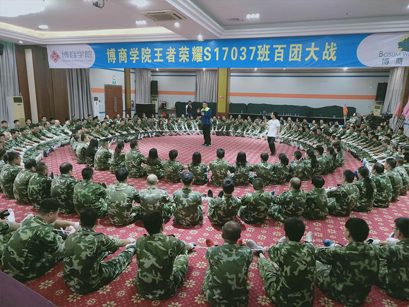
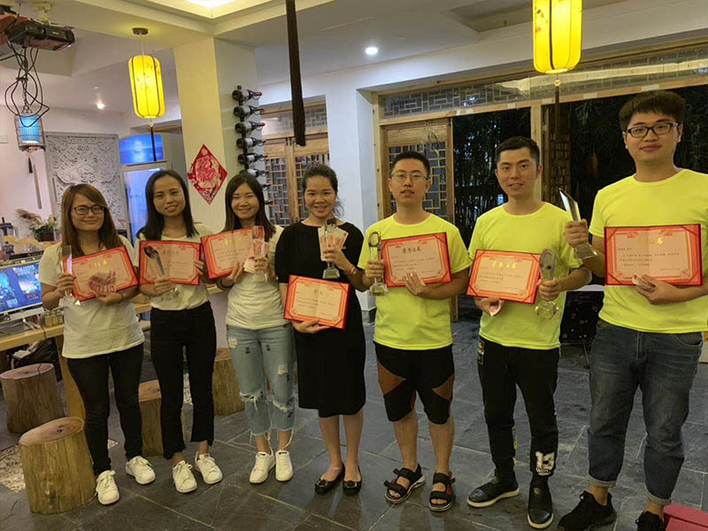
- Â Â Â Â Â Â Â Â Â Â Picture1: we are together
During the outward bound, the coach made us to feel the remarkable power of a strong team by the game. After the game, our sales team share their feelings as following:
To begin with, the leadership in a team is very important. A team without leadership just like a boat without direction, a car without wheels or a tree without leaves. In addition, the cohesiveness of a team is significant, too. The team will be a mess if the members do not in a good teamwork. As the old saying goes: “More hands makes light work.†Finally, everyone is only one of his kind. Therefore, it is required to adjust according to the member’s characteristics in the game.
 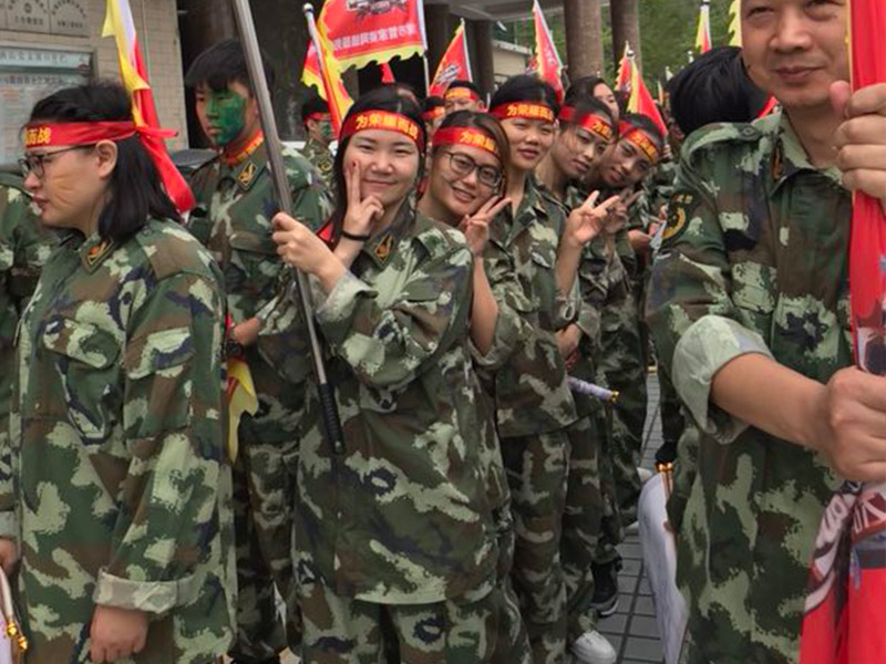
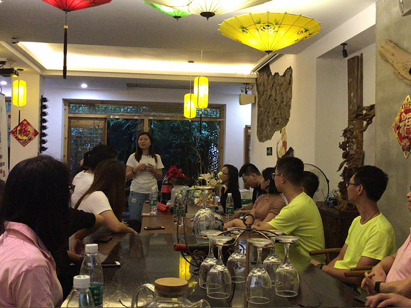
- Â Â Â Â Picture2: our sales team
Faced with many difficulties at work, sometimes we fight alone, but sometimes we need to get together and find a best way to walk out the dilemmas. Only in this way, can we meet the hope and chance.
Best, always be your best choice of PCB in China,to be customers’ best partner of printed circuit board and PCBA in China.