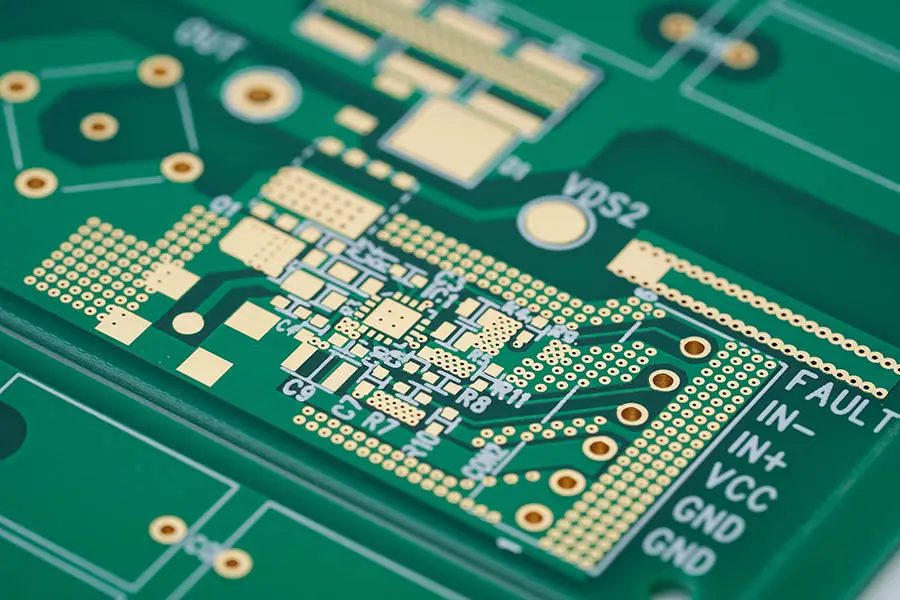
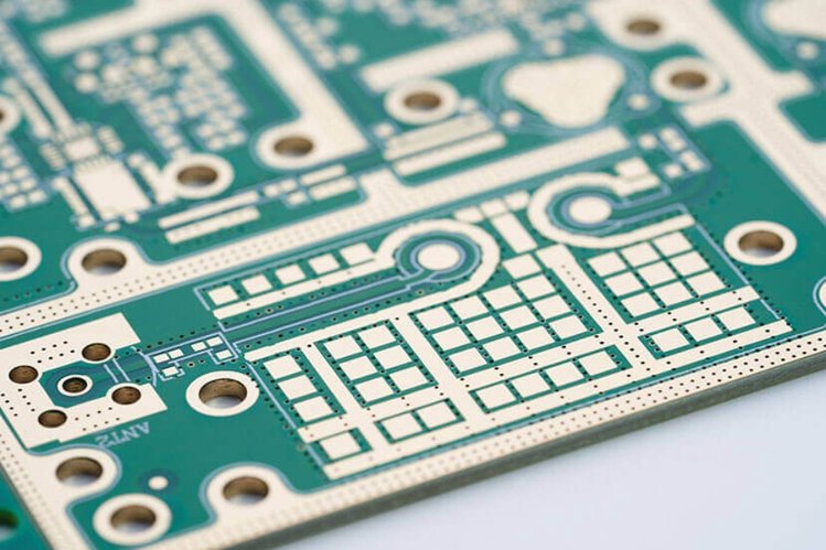
Pad on via has become a pivotal design strategy in modern high-density PCB engineering. As component pitch tightens, signal speeds accelerate, and power density increases, routing space becomes increasingly constrained, making via placement inside pads a practical solution rather than a layout preference. This article examines the engineering principles behind pad on via PCB structures, clarifies when and how the technique should be applied, and analyzes the manufacturing factors that ultimately determine solder reliability and long-term performance.
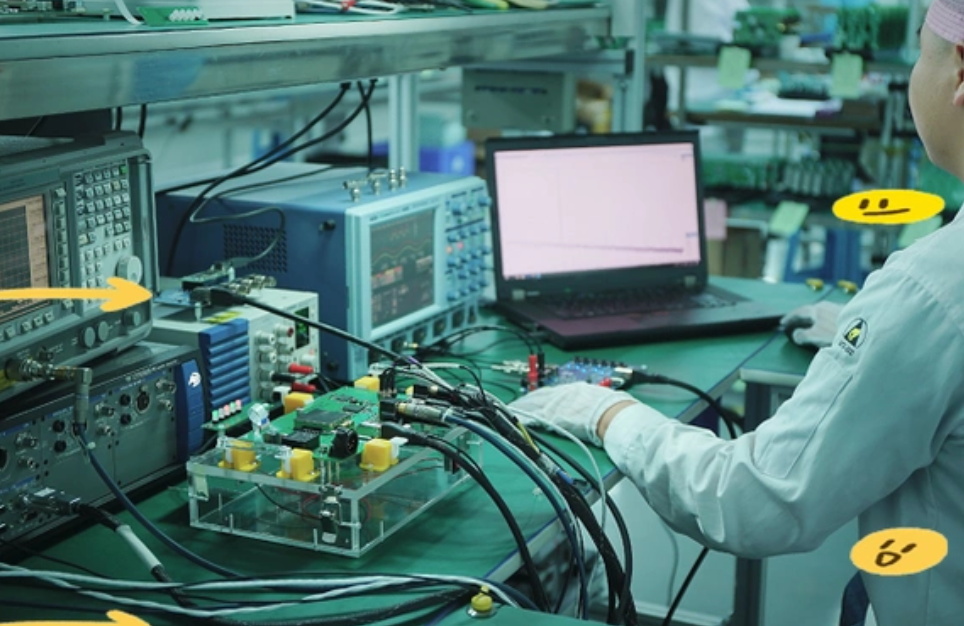
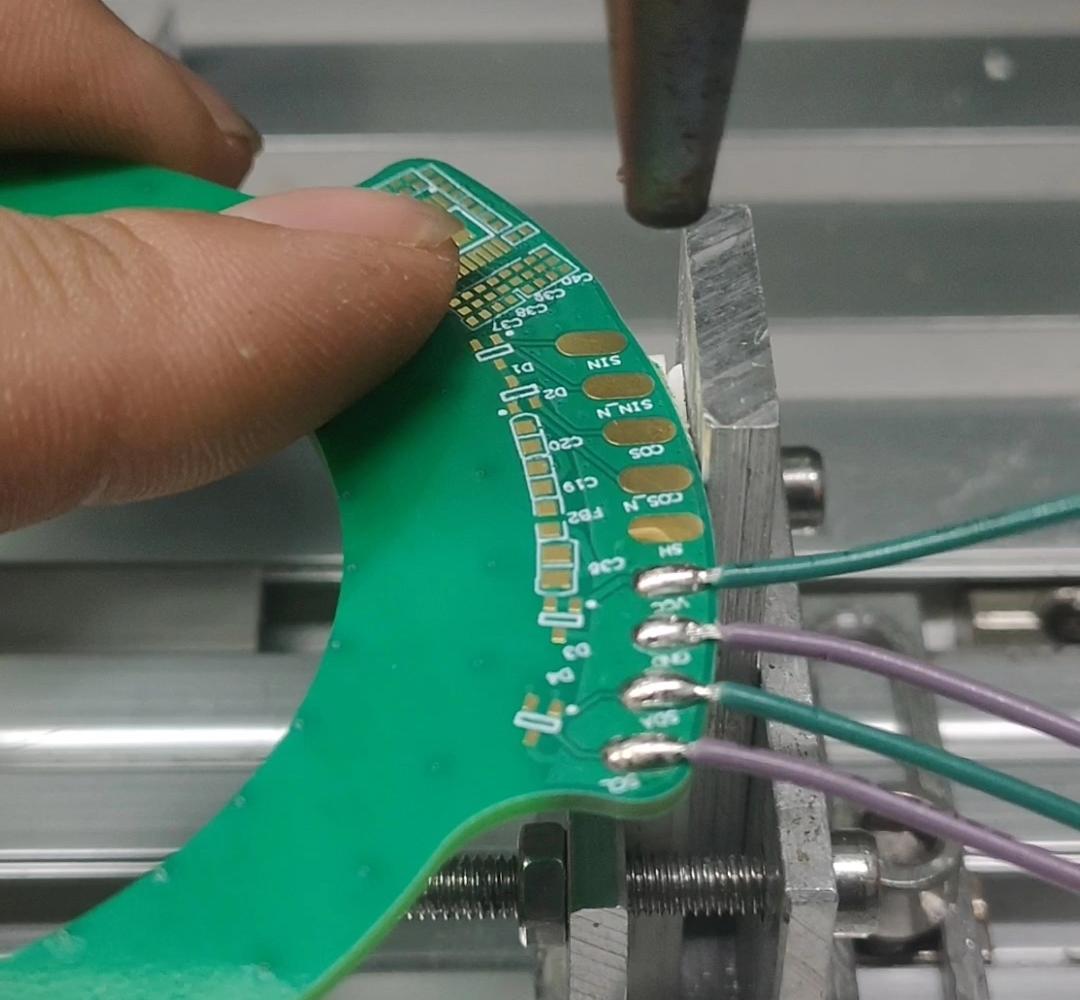
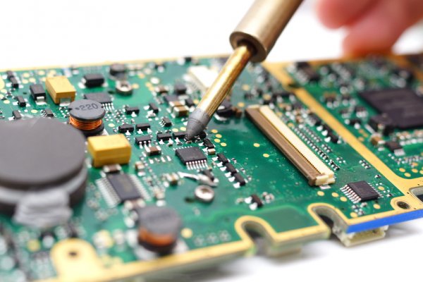
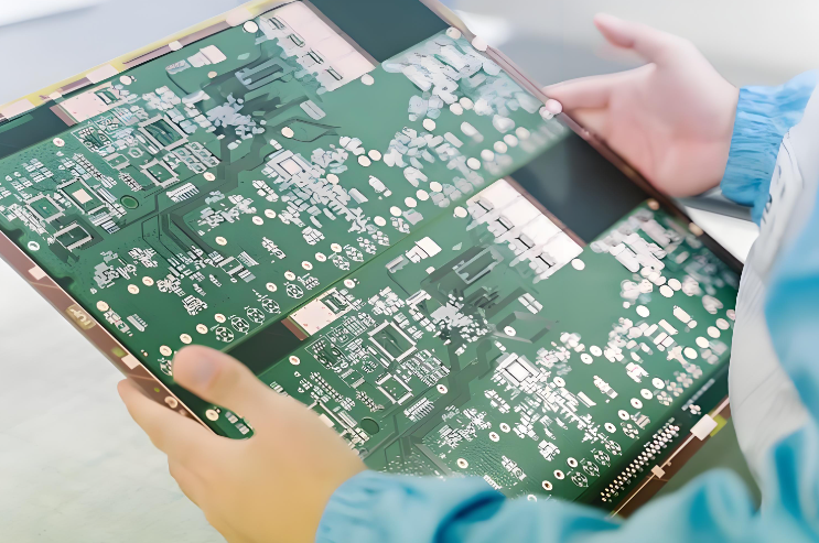
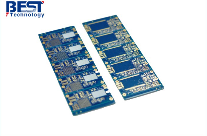
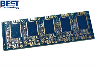
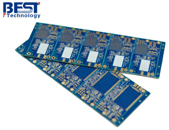
At EBest Circuit (Best Technology), advanced pad on via projects are supported by an integrated manufacturing plant equipped with complete fabrication and assembly plant systems, enabling tighter control over HDI processing and filled-via technologies. With over 20 years of experience, our team has helped customers outdo conventional routing limitations through structured DFM evaluation and process refinement. Our engineers contribute practical recommendations at the design stage, ensuring that via filling, copper capping, and planarization meet reliability expectations. Operating under ISO9001, ISO13485, IATF16949, and AS9100D quality systems, we combine certified processes with MES-driven traceability to support both prototype and production programs. For technical consultation or project discussion, please contact us at sales@bestpcbs.com.
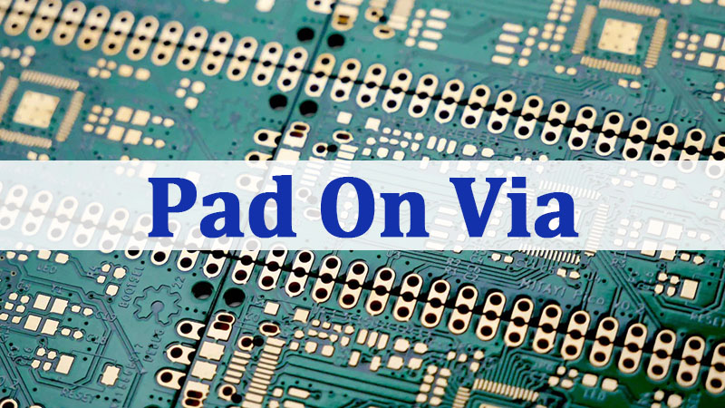
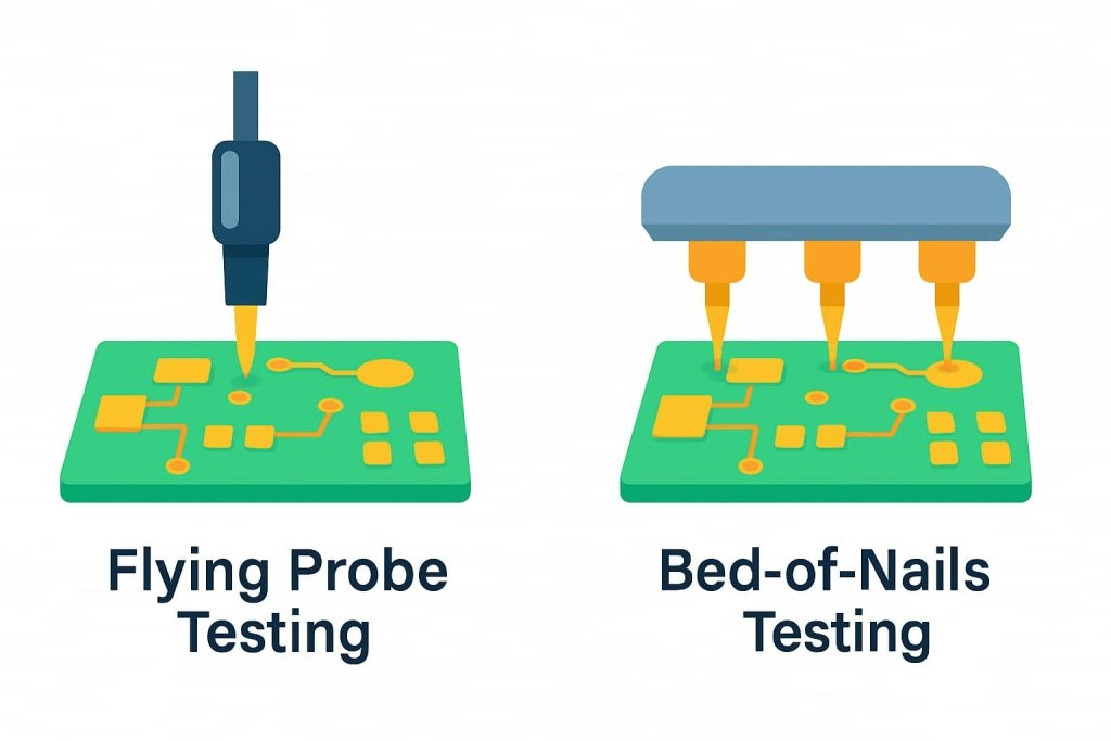
What Is Pad On Via PCB And How Does It Differ From Standard Vias?
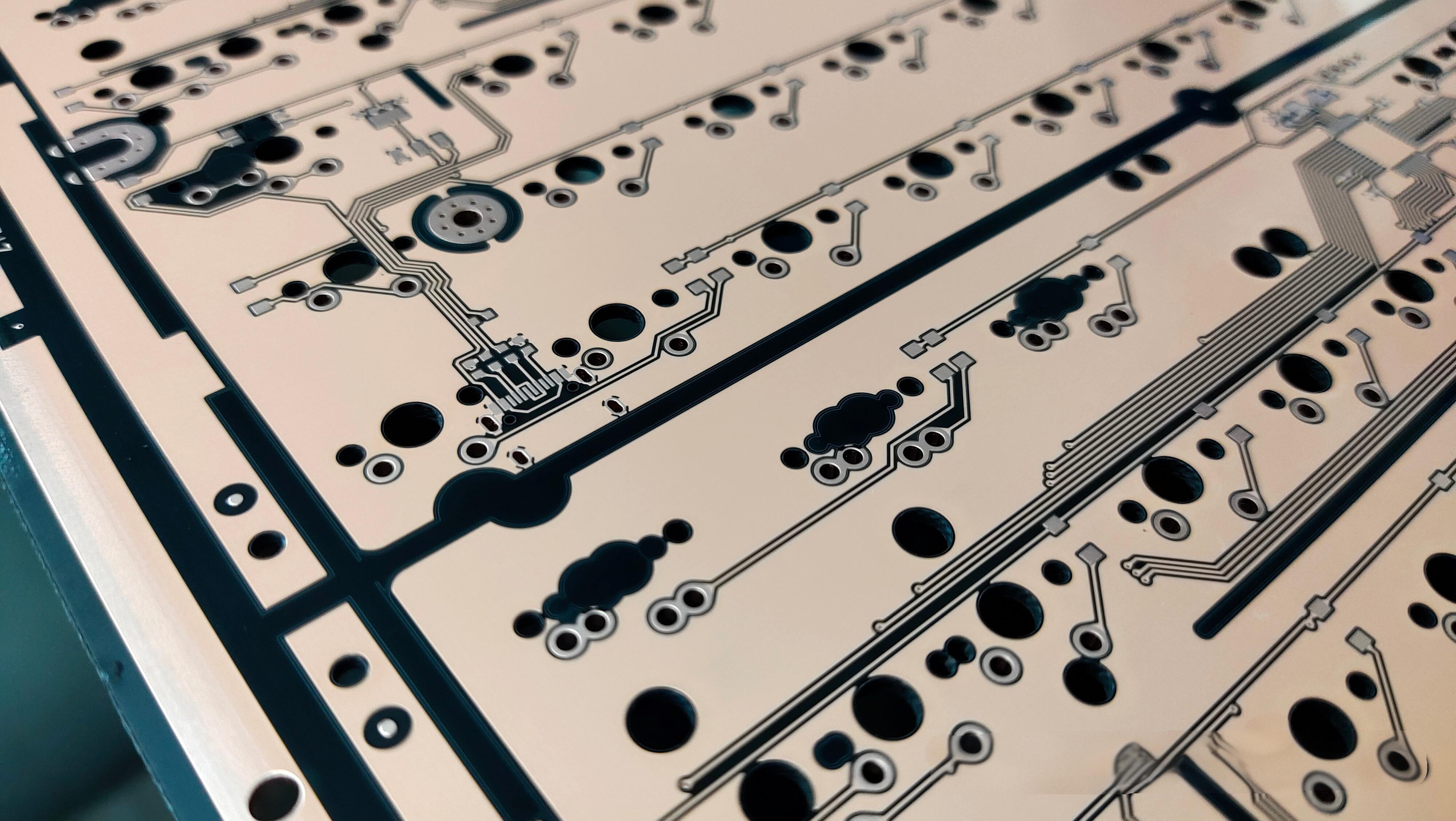
A pad on via PCB design places a via directly within the solder pad of a component. In contrast, traditional PCB layouts position vias adjacent to pads, connected by short traces.
The difference may seem minor, but it significantly impacts:
- Routing density
- Signal integrity
- Thermal dissipation
- Assembly reliability
In standard layouts, vias near pads allow solder to remain undisturbed. In via on pad PCB structures, the via barrel becomes part of the solder interface. Without proper filling or capping, solder can wick into the hole during reflow, leading to insufficient joint volume.
The primary distinction is that pad on via technology integrates vertical interconnect directly into the pad geometry, while traditional vias remain separate electrical transitions.
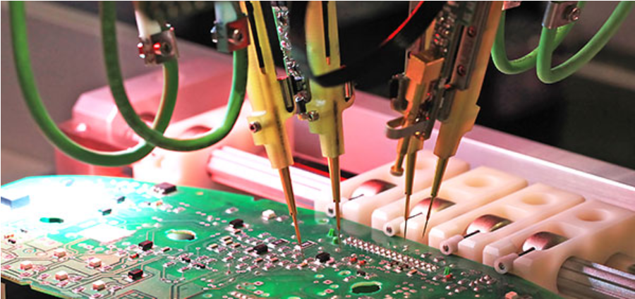
Can A Via Be Placed On A Pad In Professional PCB Design?
Yes—but not without process control.
When engineers ask whether they can place via on pad, the real question is whether the manufacturing process supports it. Simply placing vias on pads in layout software does not guarantee assembly success.
If vias are not filled:
- Solder may drain into the barrel
- Voids can form
- Component coplanarity may be affected
In professional environments, vias on pads are typically:
- Resin filled
- Copper capped
- Planarized to ensure flatness
Without these additional steps, reliability risk increases—particularly in fine-pitch assemblies.
What Is Pad On Via Technology And When Should It Be Used?
Pad on via technology refers to the engineered process of filling, plating, and planarizing vias located within solder pads to make them assembly-ready.
It should be used when:
- BGA pitch is 0.5 mm or below
- HDI structures require vertical routing efficiency
- High-speed signals demand minimal stub length
- Thermal dissipation under exposed pads is critical
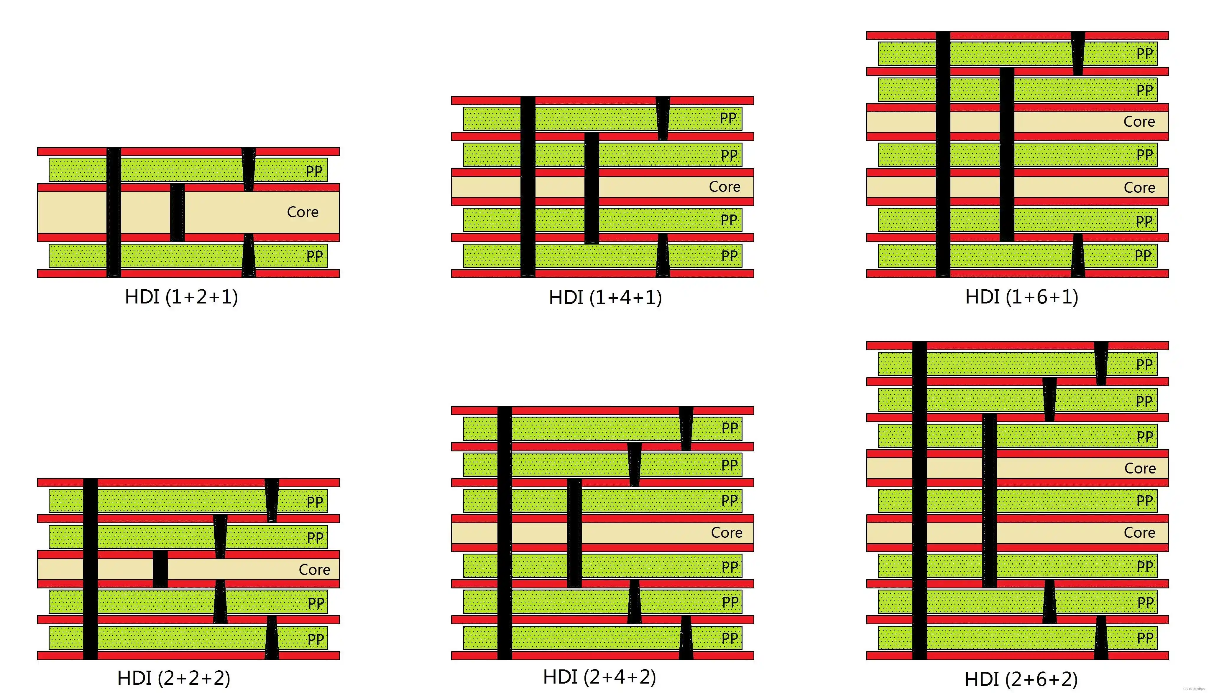
In HDI designs, especially 1+N+1 or 2+N+2 stack-ups, routing channels are limited. Using via in pad via on pad structures reduces trace escape distance and improves routing symmetry.
For power devices, vias on center pad under QFN or power ICs help transfer heat to internal copper planes.
How Does Via On Pad PCB Improve High-Density Routing In HDI Boards?
In HDI boards, trace widths and spacing shrink significantly. Traditional fan-out techniques may not work for fine-pitch BGAs.
Using via on pad PCB structures allows:
- Direct vertical escape from BGA pads
- Reduced routing congestion
- Improved signal path uniformity
This approach minimizes stub length, which benefits high-speed differential pairs and RF transitions. In fact, pad on via BGA layouts are often required for 0.4 mm pitch components.
Without this technique, routing may require additional layers, increasing cost and complexity.
Why Is Pad On Via BGA Essential For Fine-Pitch Components?
Fine-pitch BGA devices leave almost no room between pads. Routing outwards before dropping to an inner layer is often impossible.
Pad on via BGA enables:
- Immediate layer transition
- Balanced escape routing
- Reduced signal discontinuity
In high-speed digital systems, minimizing via stub length reduces reflection and impedance variation. This is particularly important in memory interfaces, FPGA designs, and high-speed serial links.
However, the mechanical reliability of PCB via on BGA pad structures depends heavily on filling and plating quality.
What Are The Via On Pad Guidelines For Reliable PCB Manufacturing?
Reliable via on pad guidelines include:
- Use filled and capped vias for SMT pads
- Maintain proper aspect ratio
- Ensure planarization tolerance within specification
- Control copper plating thickness
When placing vias on SMT pads, designers must consider solder volume balance.
For high-reliability applications:
- IPC Class 3 assemblies require strict void control
- Coplanarity limits must be maintained
Design and fabrication teams must collaborate early to align geometry with manufacturing capability.
Should Vias On Exposed Pad Be Tented Or Filled?
When working with power packages, engineers often ask whether vias on exposed pad tent or no tent is the better approach.
If left open:
- Solder may wick
- Voids may increase
If tented:
- Thermal conductivity may reduce
- Gas entrapment risk may increase
For most thermal applications, filled vias provide the best balance between heat transfer and assembly reliability. Resin filling prevents solder drainage while preserving thermal conduction through copper plating.
How Do PCB Via On BGA Pad Designs Affect Solder Joint Reliability?
The reliability of PCB via on BGA pad assemblies depends on:
- Fill integrity
- Surface flatness
- Copper plating consistency
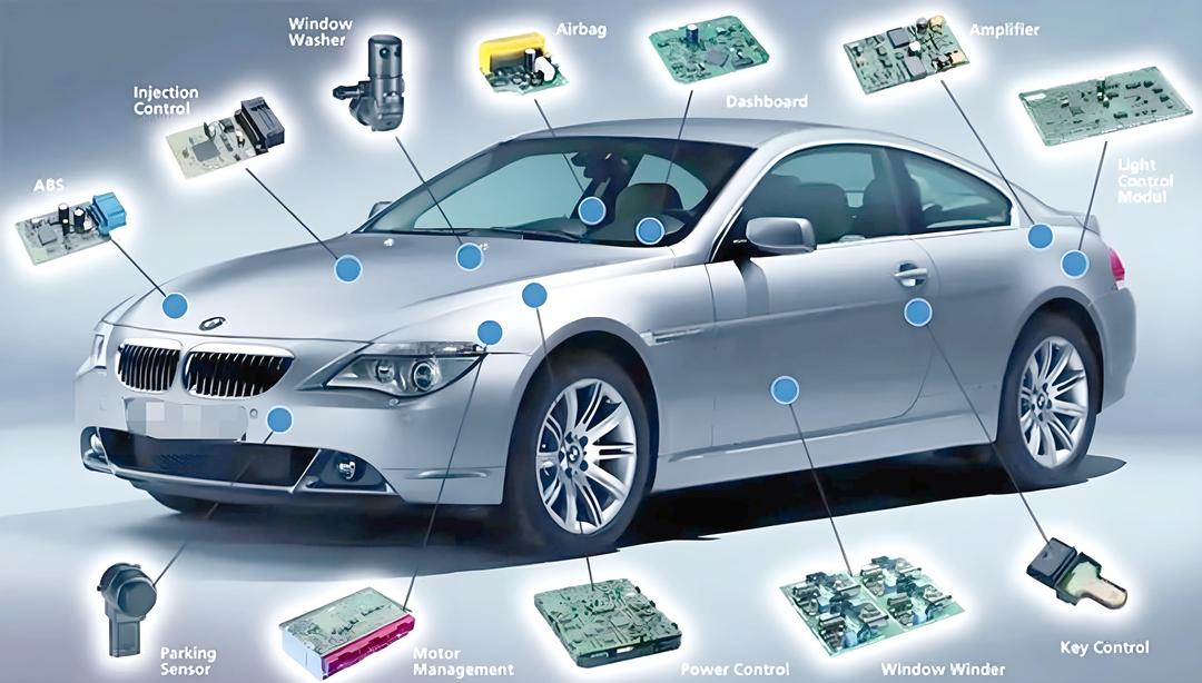
Incomplete filling can cause voiding or collapse under thermal cycling. In automotive and aerospace electronics, such failures are unacceptable.
Stress distribution across solder joints must remain uniform. Any depression or cavity from poorly processed vias can concentrate mechanical stress.
What Manufacturing Challenges Exist In Via On Pad Technology?
Via on pad technology introduces several manufacturing complexities:
- Resin fill shrinkage
- Copper cap cracking
- Surface planarization control
- Additional processing cost
Improper planarization may lead to uneven solder joints. Over-polishing may reduce copper thickness.
Moreover, vias on SMD pads require tighter process monitoring than traditional via placement.
How Does Offset Via On Pad Compare With Center Pad Designs?
In some layouts, engineers use an offset via on pad instead of placing it directly at the center.
Advantages include:
- Reduced solder wicking risk
- Improved mechanical balance
However, offset placement may introduce asymmetry in current flow or signal transition.
For high-speed signals, central placement ensures symmetric field distribution. For thermal pads, multiple vias on center pad improve heat dissipation.
Are Vias On SMT Pads Acceptable In High-Reliability Electronics?
The acceptability of vias on smt pads depends on application class.
In consumer electronics, partially filled vias may be acceptable.
In aerospace, medical, or automotive applications:
- Fully filled and capped vias are recommended
- Void percentage must be tightly controlled
- Reliability validation through thermal cycling is required
Understanding these distinctions ensures that pad on via PCB structures meet long-term durability expectations.
How To Choose A PCB Manufacturer For Advanced Pad On Via PCB Projects?
Selecting a manufacturer for pad on via pcb projects requires evaluating:
- HDI fabrication capability
- Resin filling and copper capping processes
- Surface planarization accuracy
- Inspection systems (AOI, X-ray)
- Quality certifications
Manufacturers experienced in high-density routing and IPC Class 3 production are better equipped to manage pad on via technology reliably.
In summary, pad on via technology is a powerful enabler of high-density, high-speed, and thermally demanding PCB designs. When executed properly, it improves routing efficiency, signal integrity, and heat dissipation. When implemented carelessly, it introduces reliability risk.
Design teams must evaluate not only electrical performance but also manufacturing capability before committing to via on pad PCB structures. Close collaboration between layout engineers and fabrication specialists ensures that pad on via solutions deliver both performance and durability in real-world applications. If you are evaluating pad on via PCB solutions for your next project, feel free to reach out to our engineering team at sales@bestpcbs.com for technical guidance and manufacturing support.
FAQs About Pad On Via Technology
Can Vias Be Put On Pads Without Filling?
Technically yes, but it increases solder wicking risk and reduces reliability.
What Is The Difference Between Via In Pad And Via On Pad?
The terms are often used interchangeably, though some designers differentiate between filled and unfilled structures.
Does Pad On Via Increase PCB Cost?
Yes, due to additional filling and planarization steps, but it may reduce layer count.
Are Vias On Center Pad Recommended For Thermal Relief?
Yes, especially under power components, as they improve vertical heat conduction.
Can Vias On SMD Pads Cause Solder Wicking Issues?
Yes, if not properly filled or capped.