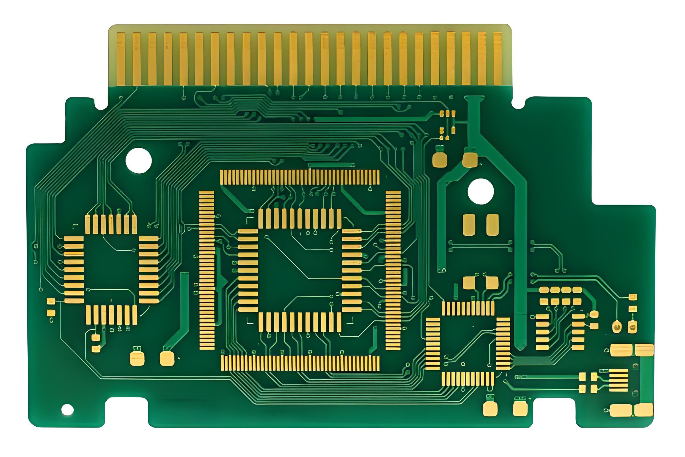
PCB panelization is a critical step in the manufacturing process that directly impacts production efficiency, material waste, and overall costs. Poor panel design can lead to lower yields, increased scrap, and delays in assembly. In this blog, we’ll explore actionable strategies to optimize PCB panelization for higher yield and cost savings.
Why Panelization Matters in PCB Manufacturing?
Panelization refers to arranging multiple PCB designs onto a single manufacturing panel (or “array”) for batch processing. Key benefits include:
Reduced material waste: Maximizing panel space utilization.
Faster assembly: Enabling automated pick-and-place machines to process multiple boards simultaneously.
Lower handling costs: Fewer individual boards to manage during fabrication and assembly.
However, suboptimal panelization can lead to:
Warpage during soldering.
V-score or routing errors.
Increased breakage during depaneling.
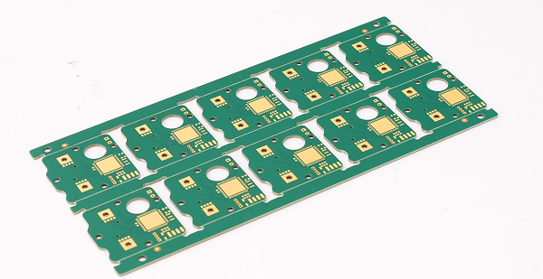
6 Tips to Optimize PCB Panelization
Base on our 19+years experiences in the PCB manufacturing field, today I would like to share you 6 Strategies to Optimize PCB Panelization
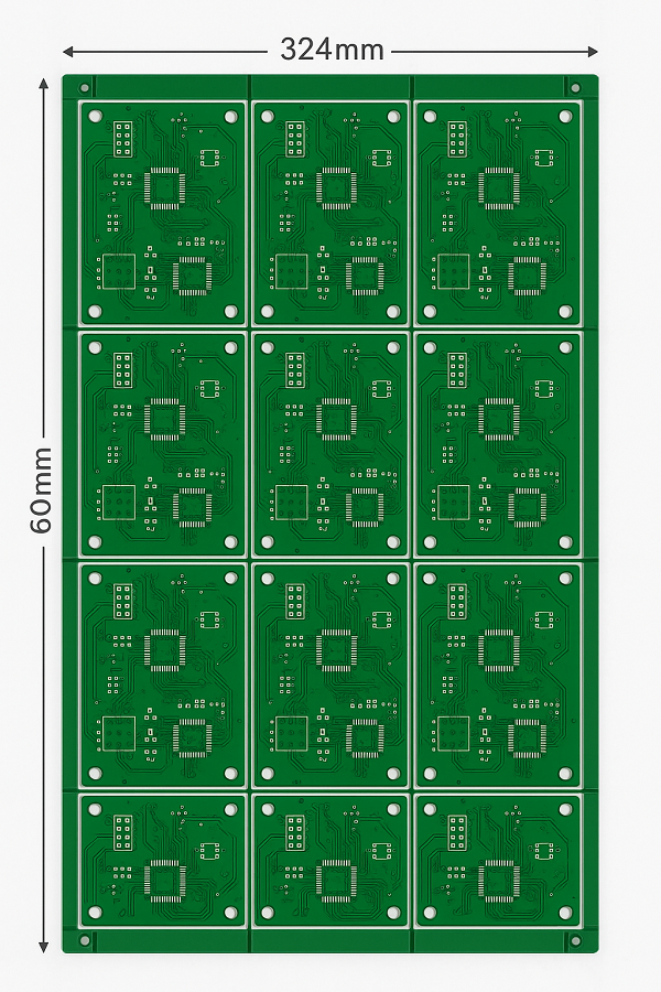
1. Choose the Right Panel Size
Align your PCB dimensions with standard panel sizes (e.g., 18″x24″, 21″x24″) to minimize material trimming.
Example: If your board is 80mm x 60mm, arrange 4×6 units on a 324mm x 480mm panel to reduce unused space.
2. Optimize Board Arrangement
Rotation: Rotate boards to fit more units per panel.
Mirroring: Use symmetrical designs to avoid “wasted” gaps.
Nesting software: Leverage tools like CAM350 to automate optimal layout generation.
3. Select the Best Depaneling Method
The choice of depaneling (separating individual boards) affects yield and edge quality:
V-Score: Low cost and fast, but requires straight edges and may weaken boards.
Tab Routing: Ideal for irregular shapes but adds milling time.
Laser Cutting: Precision for high-density designs, but higher cost.
Rule of thumb: Use V-score for rectangular boards and routing for complex shapes.
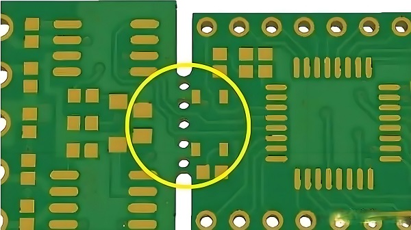
4. Add Breakaway Tabs and Mouse Bites
Breakaway tabs: Small connectors between boards to prevent movement during assembly.
Mouse bites: Perforated holes for easy manual separation.
Spacing: Maintain 1.5–2mm between boards to avoid solder mask bridging.
5. Incorporate Fiducials and Tooling Holes
Add global fiducials to the panel for accurate alignment during SMT assembly.
Include tooling holes (3.2mm diameter) to secure the panel during drilling and routing.
6. Balance Quantity vs. Risk
Overcrowding panels increases the risk of cross-board defects.
Underutilizing panels raises material costs.
Recommended: Aim for 4–20 boards per panel, depending on size and complexity.
Case Study: Cost Savings Through Smart Panelization
A consumer electronics manufacturer redesigned their 50mm x 50mm IoT module panel:
Initial design: 8 boards/panel with 15% wasted space.
Optimized design: 12 boards/panel using rotated layouts and shared tooling holes.
Results:
15% reduction in material costs.
10% faster SMT assembly.
Fewer depaneling errors due to improved tab routing.
Common Panelization Mistakes to Avoid
Ignoring manufacturer capabilities: Always consult your PCB fab’s panel size and tolerances.
Overcomplicating shapes: Complex panels increase milling time and scrap rates.
Skipping test coupons: Include test patterns for impedance control and quality checks.
Conclusion
Optimizing PCB panelization requires a balance of geometric efficiency, process knowledge, and collaboration with manufacturers. By implementing these strategies, you can reduce waste, improve yields, and lower production costs without compromising quality.
Pro Tip: Use panelization-specific design rules in tools like Altium or KiCad to automate compliance checks.
Also, if you want to know more about how to optimize PCB Panelization for Higher Yield and Lower Cost, please feel free to inquiry from us.
Have you ever wondered what powers your mobile phone behind the screen? Every tap, swipe, or call you make is possible because of one hidden hero: the mobile phone PCB. In simple terms, the mobile circuit board connects and controls all parts of your phone. It links the battery, screen, camera, processor, and even your wireless network. Without it, nothing would work.
At EBest Circuit (Best Technology), we design and manufacture custom mobile PCBs that support today’s advanced smartphones. As a leading mobile PCB manufacturer both in China and Vietnam, we have decades years of experience in producing high-quality boards for mobile devices, wearables, and smart electronics. Certificated by ISO9001, IATF16949, ISO13485, AS9100D, it shows we have enough capability to produce highest quality mobile PCB board. Whether you need flexible, rigid, HDI, RF or multilayer PCBs, we deliver one-stop solutions with fast turnaround and competitive pricing.
What Is a Mobile Phone PCB?
A mobile phone PCB is the core of your smartphone, which drives your phone be intelligent. It looks like a green or black plate populated with many small electronic parts. These components are connected through thin copper lines etched onto the board. Together, they power your phone and make sure each part works smoothly.
In smartphones, the PCB board mobile phone is usually a multi-layer board, meaning it has several layers stacked together. This design helps save space and supports high-speed data processing. The PCB also holds all essential parts like the processor, memory, charging port, and wireless chips.
What Does a Mobile Phone PCB Actually Do?
A mobile phone PCB acts like the brain and nervous system, it mainly used to connect and manage every part of the phone, its working principle is:
Power distribution: It sends power from the battery to other parts.
Signal transmission: It lets the processor talk to the screen, camera, and sensors.
Component support: It holds everything in place and keeps them working together.
Without the mobile phone PCB, the battery wouldn’t know how to charge, the screen wouldn’t respond, and the speaker wouldn’t play music. It handles all the behind-the-scenes activity while you use your apps and make calls.
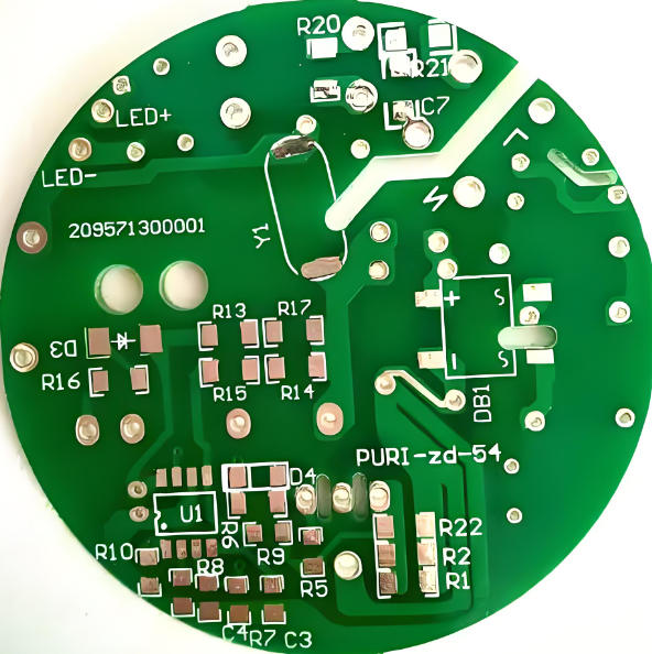
Core Components on a Mobile Phone PCB
A mobile phone PCB always is a populated PCB. At the top of the PCB, you’ll find the antenna point, where the antenna connects. Your phone connects to Wi-Fi, Bluetooth, and cellular networks through these antennas. Each component on the PCB plays its unique role:
Antenna Switch: A 16-leg switch that controls signal direction. Sometimes built together with the PFO.
PFO (Power Frequency Oscillator): Manages signal frequency. Found next to the antenna switch.
Network IC: Controls mobile network functions. In some phones, it’s built into the CPU.
Power IC: Found near brown capacitors. Regulates power across the PCB.
CPU (Processor): The largest IC. Handles all system commands and performance tasks. Some phones have two CPUs.
Flash IC: Stores system data and software. Located beside the CPU.
Logic IC: A 20-pin chip. Manages basic logic operations.
Charging IC: Found beside R22. Controls battery charging.
Audio IC: Controls sound functions. Placed close to the Power IC.
Capacitors: Store and release electrical energy. Help stabilize power supply.
Resistors: Control the flow of current. Protect other parts from too much power.
Diodes: Allow current to flow in one direction only. Prevent power damage and signal errors.
Below is a multi-layer PCB used in iphone. These parts make it possible for you to browse, take photos, and connect with the world.
Why Multi-layer PCBs Are Standard in Smartphones?
Today’s smartphones are like mini computers. They handle everything from streaming video to running powerful apps. To keep up, mobile phone PCB design has evolved. One of the biggest upgrades? The switch to multi-layer PCBs. Here we listing main advantages of using multi-layer PCBs in mobile phone.
Firstly, multi-layer PCBs offer higher circuit density, allowing more components like processors and memory to fit in the limited space. For example, the iPhone 14 Pro uses a 10-layer PCB to deliver powerful functionality in a compact design.
Secondly, they improve high-speed signal transmission by reducing interference through ground and shielding layers, ensuring stable and fast data transfer—a must for modern smartphones.
Additionally, multi-layer PCBs reduce the size and weight of smartphones. By accommodating more circuits in the same area, they help achieve smaller, lighter designs, like in the Apple Watch Series 8.
Finally, multi-layer PCBs enhance reliability and mechanical strength. Their complex construction improves durability and vibration resistance, ensuring a longer-lasting product.
How Inner and Outer Layers Interact in a Mobile PCB Stack?
In a mobile PCB board, the inner and outer layers work together like a team. The outer layers handle the connection of chips, antennas, and components you can see. Meanwhile, the inner layers manage signal traces, power distribution, and ground planes.
Signals often travel between these layers through vias—small holes filled with metal that link one layer to another. This allows for faster, cleaner communication between the mobile PCB components, such as the CPU, RAM, and radio circuits.
Materials Used in Mobile PCB Board
Choosing the right materials is crucial in mobile phone PCB manufacturing. Each layer and part of the board serves a different purpose, so engineers carefully select materials to match performance needs, durability, and size constraints. Here’s a comparison of commonly used mobile PCB materials:
Material
Description
Pros
Common Use in Mobile PCB
FR4
Fiberglass-reinforced epoxy laminate
Cost-effective, stable electrical properties
Base material in most mobile PCB cores
Polyimide
Flexible and heat-resistant material
Great for flexible PCBs and foldable applications
Used in camera modules, folding phones
Rogers
High-frequency laminate
Low dielectric loss, excellent RF performance
Antenna sections, 5G, Wi-Fi, Bluetooth
Teflon (PTFE)
Non-stick, high-performance polymer
Ultra-low signal loss, ideal for high-speed signals
Used in high-speed communication layers
Ceramic
Advanced inorganic composite
Excellent heat dissipation, high frequency stability
Power modules, 5G RF front-end, shielding
PCB Layout Basics for Mobile Phones
A solid layout is the backbone of any mobile phone PCB. Designers start with the schematic, which maps every component and connection. Mobile PCB layout focuses on a few key goals:
Short signal paths to avoid delay.
Clear power and ground planes for stability.
Thermal zones to manage heat.
Shielded areas for RF sections like Wi-Fi and GSM modules.
Placing the processor, RAM, power management ICs, and antennas carefully prevents problems later.
Warm tips:
Keep power and ground layers as solid planes. Avoid breaks or thin sections, which create voltage drops. Also, decoupling capacitors should sit close to power pins of chips.
Tips for GSM, Wi-Fi, Bluetooth, and 5G Mobile PCB Antennas
Keep antennas away from metal—metal blocks signals.
Use ground clearance around antenna traces to reduce noise.
Match impedance of the RF trace to avoid reflection.
Add shielding near high-speed digital lines to prevent signal loss.
For 5G, which uses millimeter-wave bands, the routing must be super precise. Even a few millimeters can affect signal strength. Tools like electromagnetic simulation software help refine these paths.
How AI and Automation Are Changing PCB Layout?
AI and automation have brought big changes to mobile PCB design in this two year. Instead of placing parts manually, designers can now rely on smart layout tools that optimize paths automatically. Machine learning predicts optimal routing paths. Automation assists in component placement, thermal analysis, and EMI reduction. They suggest better placements in seconds—saving hours of work.
AI also speeds up mobile PCB testing. It spots defects on boards using image recognition. That means more accurate inspections, less rework, and faster production.
As AI tools improve, they’ll continue to reduce errors, cut costs, and deliver better mobile board designs. It’s a leap forward for the industry.
What Does EBest Circuit (Best Technology) Serve You?
At EBest Circuit (Best Technology), we provide complete solutions for mobile PCB design and manufacturing. Whether you’re developing a new smartphone, tablet, or wearable device, we help you build it from the ground up. Our services including but not limited to:
Custom mobile phone PCB layout and design based on your needs
Single-layer to 32+ layer boards, including HDI, rigid-flex, and high-frequency options
Advanced material selection such as FR4, polyimide, Rogers, and BT epoxy
Rapid prototyping and small-volume production with quick delivery
Full testing services like AOI, flying probe, impedance, and X-ray inspection
With over 18 years in the PCB industry, we’ve supported top-tier brands in building reliable, high-performance mobile electronics. Our team works closely with customers and give the best suggestions to optimize your mobile circuit board design. If you are interested in the mobile PCB develop, you are welcome to contact our team at sales@bestpcbs.com.
FAQs
1. What does a mobile phone PCB diagram show?
It shows where each component is placed on the board and how they are connected through copper traces.
2. How can I avoid power issues in PCB layout?
Use ground planes, short power paths, and place capacitors close to chips for voltage stability.
3. How do I identify damaged parts on a mobile PCB?
Use thermal cameras, multimeters, and reference schematics to locate shorted, burned, or faulty components.
4. What makes EBest Circuit (Best Technology) a strong mobile PCB manufacturer?
They provide full-stack design-to-production all in one service, expert engineering support, DFM check, SI, PI analysis and a proven track record in mobile electronics.
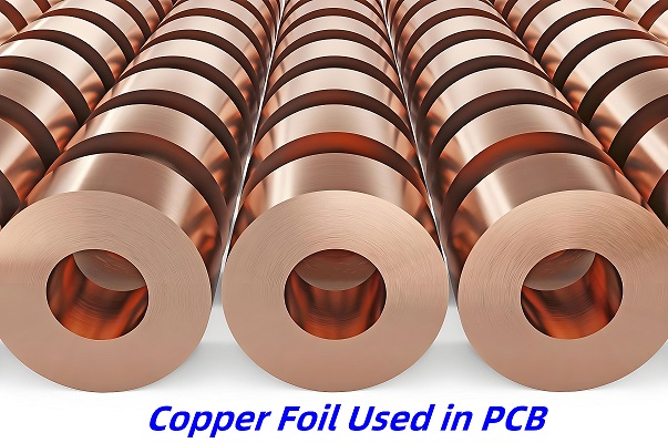
A copper foil PCB is a type of printed circuit board where copper foil is laminated onto the base material to form the conductive layer. This copper layer is what carries electrical signals and power between different parts of the board. Without it, a PCB wouldn’t function at all.
The copper is typically applied through lamination, where thin sheets of copper foil are bonded to a substrate, usually made of fiberglass-reinforced epoxy resin like FR4. This copper layer is then etched to create precise paths, known as traces, that connect components across the board.
There are also different thicknesses of copper foil used, which affect the board’s ability to carry current and dissipate heat. The standard thickness is usually 1 oz/ft² (about 35μm), but heavier copper options like 2 oz or 3 oz are often used in power electronics or high-temperature applications.
What is the Purpose of Copper Foil in PCB?
The main role of copper foil is to carry electric current across the circuit. It’s the path for data, signals, and energy. Without copper foil, there would be no communication between components.
Besides that, copper foil helps in thermal transfer. When current flows, heat is generated. Copper helps in spreading this heat evenly, reducing hot spots. That’s key in designs with dense parts or power-hungry chips. Also, copper layers add mechanical strength to the board, supporting solder joints and reducing flex.
What are the Different Types of Copper Foils?
Copper foil types vary based on how they’re made, how rough they are, and what kind of performance they offer in real PCB applications. Choosing the right type can make a big difference in signal clarity, layer adhesion, and long-term reliability. Let’s see the most common types used in the PCB industry:
1. Electrodeposited (ED) Copper Foil
Electrodeposited copper foil is the most widely used type in standard rigid PCBs. It’s made through an electrochemical process where copper ions are deposited onto a rotating stainless steel drum. The side in contact with the drum becomes smooth, while the other side is naturally rough.
ED copper foil is great for multilayer rigid boards, consumer electronics, and automotive circuits. When treated with surface chemicals, it bonds well to laminates and resists layer separation.
2. Rolled Annealed (RA) Copper Foil
RA copper foil is made by mechanically rolling solid copper into very thin sheets and then annealing it (heating and cooling) to relieve stress. You’ll find RA copper in flex circuits, flex-rigid PCBs, wearable electronics, and mobile devices. When boards must flex without breaking, RA is the go-to.
3. Reverse Treated Foil (RTF)
RTF is a type of ED foil where the shiny side is treated instead of the rough side. This treatment adds micro-etching or chemical bonding to enhance adhesion between the copper and the laminate. RTF is popular in HDI (High-Density Interconnect) boards, high-speed digital circuits, and RF designs where signal loss must be controlled.
4. Very Low Profile (VLP) and Ultra-Low Profile (ULP) Copper Foils
These are smoother versions of standard ED foils, created to reduce conductor roughness. VLP and ULP foils are still electrodeposited, but they go through extra steps to minimize surface peaks and valleys. They are used in high-speed digital systems, data centers, 5G antennas, and any application where clean signal transmission matters.
5. High-Temperature Elongation (HTE) Copper Foil
HTE copper foil is a variant of ED copper, enhanced for high thermal and mechanical stress. It resists cracking under repeated heating and cooling cycles. HTE is preferred for automotive, power electronics, and multilayer PCBs that go through reflow soldering or see high current loads.
6. Resin-Coated Copper Foil (RCC)
RCC combines copper foil with a thin layer of resin. This resin bonds directly to the core without needing prepreg sheets, which simplifies the lamination process. Mainly in mobile phones, compact devices, or where thin layers and high accuracy are needed.
Here is a summary comparison table between them:
Copper Foil Type
Strength
Flexibility
Smoothness
Signal Performance
Application
ED
High
Low
Moderate
Standard
Rigid PCBs
RA
Medium
High
High
Good
Flex PCBs
RTF
High
Medium
Treated
Excellent
RF, HDI
VLP/ULP
Medium
Medium
Very High
Superior
5G, high-speed
HTE
Very High
Low
Moderate
Standard
Power boards
RCC
Low
Medium
High
Good
Thin mobile boards
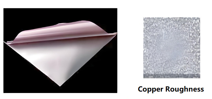
What is the Roughness of Copper Foil in PCB?
The roughness of copper foil on PCB refers to the unsmoothness of the copper foil surface, Copper foil roughness affects how well signals move through the board. In high-speed designs, surface texture matters a lot. Rough copper increases insertion loss. This weakens the signal and causes noise.
Roughness is usually measured in microns, which is usually quantified by Ra, Rz and Rq. Lower values are better for RF or high-speed data.
Ra: The arithmetic average of the absolute value of the contour deviation over the sampling length, applicable to copper foil surface.
Rz: Sum of the average of the 5 largest profile peak heights and the average of the 5 largest profile valley depths over the sampling length for copper foil rough surface.
Rq: Means RMS (Root means square) value, it also is a roughness index.
PCB Copper Thickness Chart
Copper thickness is often given in ounces per square foot. But that doesn’t mean much until you convert it. Here’s a helpful chart:
Copper Weight (oz/ft²)
Thickness (µm)
Thickness (mil)
0.5 oz
~17 µm
~0.67 mil
1 oz
~35 µm
~1.37 mil
2 oz
~70 µm
~2.74 mil
3 oz
~105 µm
~4.11 mil
4 oz
~140 µm
~5.48 mil
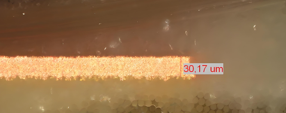
For single & double sided PCB, the copper foil thickness is about 35um, 50um, 70um;
For multi-layer PCB, its outer layer copper thickness is 35um, and inner layer copper thickness is 17.5um (1/2oz).
Designers choose copper weight based on current flow and thermal limits. Thicker copper is used in power PCBs. Thinner layers are more common in signal circuits or HDI boards.
HTE vs RTF copper foil
When it comes to choosing the right copper foil for high-performance PCBs, HTE (High-Temperature Elongation) and RTF (Reverse Treated Foil) are two of the most commonly used options.
HTE Copper Foil
HTE copper foil is a specially processed electrodeposited foil that’s engineered to handle high thermal and mechanical stress. The term “high-temperature elongation” refers to the foil’s improved flexibility and stretch resistance when exposed to heat.
It’s treated chemically to improve adhesion strength, making it more reliable during multiple soldering cycles. The surface has a consistent profile that bonds well with different dielectric materials.
Key Features of HTE Foil:
Strong peel strength
Durable under repeated heating
Excellent for plated-through-hole (PTH) reliability
Withstands lamination and solder reflow cycles
RTF Copper Foil
RTF, or Reverse Treated Foil, is also made through an electrodeposition process, but with one key difference: the shiny side gets treated instead of the rough side. This treatment applies a fine, uniform microstructure that enhances bonding without creating high surface roughness.
This smoother surface makes RTF a preferred option in high-speed signal and RF PCB applications where low signal loss is critical.
Key Features of RTF Foil:
Lower surface roughness
Better electrical performance at high frequencies
Improved signal integrity
Balanced peel strength and performance
PCB Copper Electrical Conductivity
Copper has one of the highest electrical conductivities of any metal. That’s why it’s the go-to choice for PCBs. The typical conductivity of copper used in PCBs is about 5.8 x 10⁷ S/m (Siemens per meter).
This high conductivity allows small traces to carry high current with low voltage drop. It also reduces signal distortion, which is key in high-speed or RF applications.
Still, conductivity depends on purity. Most PCB foils use 99.9% pure copper. If copper is oxidized or poorly handled, conductivity drops. That’s why clean processes and proper lamination are important.
How to Calculate Copper Thickness in PCB?
The thickness of copper in PCB can be calculated by the following methods:
1. Calculation of copper plating thickness by current density and plating time:
Plating thickness (um) = current density (ASF) x plating time (min) x plating efficiency × 0.0202. This formula takes into account the amount of electricity, equivalent, molar mass, density and other factors. The specific calculation process involves the product of current density, plating time and plating efficiency, then multiplying by a factor 0.0202.
2. Thickness calculated by weight of copper foil:
In the common option “copper-covered FR4, single-sided,1 oz”,1 oz indicates the thickness of the copper foil. 1 oz = 28.35 g/ft², copper foil density of 8.93 g/cm³, 1 square foot = 929.03 cm². Thus, 1 oz copper foil thickness = 28.35/8.93/929.03 ≈ 35um or 1.35mil . Common PCB thicknesses include 1/2Oz = 17.5um, 1 oz = 35um, 2oz = 70um, and 3 oz = 105um.
1. Isola Group:Known for high-frequency and low-loss materials.
2. Kingboard: One of the world’s biggest copper clad laminate suppliers.
3. Ventec International: Offers low-profile copper foils and thermal substrates.
4. Mitsui Mining & Smelting: A top name in RTF and ultra-smooth foils.
5. EBest Circuit (Best Technology): Based in Asia, with 18+ years in the industry. We supply high-quality copper foil PCBs, from 0.5 oz to over 6 oz.
At EBest Circuit (Best Technology), we bring over 18 years of hands-on experience. We support standard and custom copper weights, including heavy copper for high-current boards. Our RTF and HTE options fit both signal-sensitive and power-heavy needs.
With fast lead times, in-house testing, and global delivery, we’re more than just a PCB maker. We’re your reliable partner for copper foil PCB solutions. Reach out today to explore your next project with confidence.
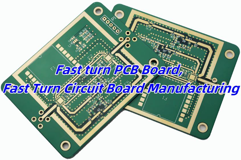
A fast turn PCB board is a printed circuit board manufactured and delivered in a short time, typically within 24 to 72 hours. These quick deliveries help speed up product development, especially during prototyping and pre-production stages. It’s a solution many engineers rely on when time is tight.
Engineers use fast turn PCBs for product validation. They want to see if a new circuit design performs well before moving to mass production. So, getting a board in days instead of weeks can make a huge difference.
First, it speeds up your product timeline. You don’t need to wait weeks to test your circuit. If changes are needed, you can get a revised board quickly and keep things moving forward.
Second, it helps reduce project risks. The faster you test, the faster you detect potential design errors. Early detection saves money and prevents delays.
Third, it improves decision-making. With working samples in hand, your team can test real performance. It’s better than guessing or using simulation data only.
Lastly, fast turn options give your company a competitive edge. Getting to market faster often means better sales and stronger customer trust.
EBest Circuit (Best Technology)’s Typical Turnaround Time for Fast Turn PCBs
At EBest Circuit (Best Technology), we understand the value of time. That’s why we’ve optimized our process to support urgent PCB orders.
For standard 2-layer fast turn PCBs, we usually deliver in 24 to 48 hours. For 4-layer boards, it may take 48 to 72 hours depending on complexity. Our team works around the clock to meet those deadlines.
Even for more complex boards — such as HDI or metal-core PCBs — we still maintain one of the quickest turnaround times in the industry. And we don’t compromise on quality. Each board goes through full inspection and electrical testing before it reaches you. The detailed turnaround time is:
Prototype(<1m²)
Layers
Normal Service
Expedited Service
FR4 PCB
1 Layer
3-4 days
24 hours
2 Layers
4-6 days
24 hours
4 Layers
8-10 days
48 hours
6 Layers
8-10 days
72 hours
8 Layers
10~14 days
72-96 hours
10 Layers
14-18 days
72-96 hours
HDI (1+N+1 2+N+2)
2.5 – 3.5weeks
TBD (depend on design)
We don’t just print boards fast. We manage the process with strict planning, from materials to delivery. That’s why so many clients come back to us for every new project.
Factors That Affect the Turnaround Time of Prototypes
Even though we push for speed, several factors can influence how long a fast turn circuit board takes to produce. Knowing these helps avoid delays.
Circuit Board Design and Test Procedures
The design stage impacts everything. A simple, well-structured layout speeds up processing. Complex routing, fine-pitch components, or tight spacing can add extra review time.
Test procedures matter too. If a special test is needed, like impedance control or functional test setup, it adds to the schedule. Providing clear instructions in advance helps us prepare and avoid delays.
Lamination Cycles
For multilayer boards, each lamination cycle takes time. A 4-layer multi-layer board needs one cycle, while an 8-layer may need several. More layers mean longer pressing times and more careful control.
Quick builds still go through these steps. We just start immediately and plan shifts to manage it faster. That’s why sharing the full stack-up early is so important.
Via-in-Pad Plated Over
Via-in-pad designs are helpful for high-density layouts. But they add a few extra steps in production. We need to drill, plate, and fill those vias carefully. After that, we cap and flatten them before plating the surface.
This extra effort adds time compared to standard vias. If your board uses VIPPO, it’s best to let us know upfront so we can fast-track these processes.
Fabrication Drawing Specifications
Precise drawings help avoid back-and-forth communication. If drawings are unclear or missing details like dimensions, tolerances, or hole types, we’ll need to clarify before production.
Clear drawings lead to fast fabrication. They also reduce the risk of mistakes. That’s why we suggest using IPC-2581 or Gerber X2 format with notes included.
Surface Finish
Surface finish choice also plays a role. ENIG, OSP, HASL, or hard gold all have different process times. For example, ENIG takes longer than HASL because it involves two plating steps.
If speed matters most, we can recommend the best finish based on your needs. Some finishes can still meet performance goals while shaving off hours from the process.
Assembly Drawings and Notes
If you also need PCB assembly, complete documentation is key. Missing part placements, unclear polarity marks, or unreferenced BOM items slow everything down.
Providing all files in one go—BOM, pick and place, centroid file, and notes—helps avoid delays. When everything’s ready, our SMT line can move fast and precise.
Fast Turn Circuit Board Manufacturing
Manufacturing a fast turn circuit board isn’t about rushing. It’s about knowing how to work smart, reduce waste, and prevent rework.
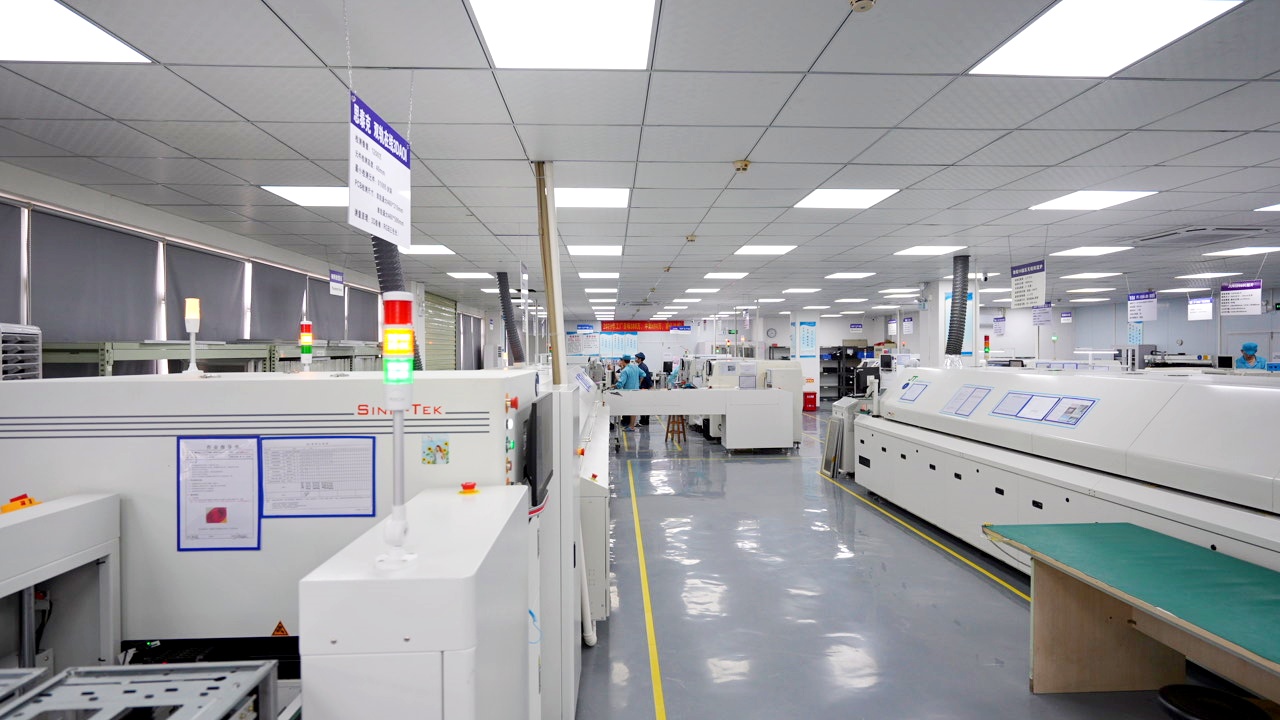
At EBest Circuit (Best Technology), we keep a reserve stock of core materials and prepreg. That way, we can start production immediately without waiting for supply.
We also use automatic routing, inline AOI, and robotic drilling machines to keep operations smooth. Our teams work in shifts, so production doesn’t stop, even at night or on holidays.
Every department is synchronized. CAM engineers review your files fast, material control prepares the stack-up, and QA teams check every step. That’s how we manage fast output without losing accuracy.
We also run a parallel system for urgent jobs. These special jobs go into our “fast-lane” line, separated from standard orders. This ensures time-sensitive boards don’t get stuck behind large-volume orders.
Why Should You Choose EBest Circuit (Best Technology) as Your Preferred Partner?
Experienced team: We’ve been in this field for over 18 years. Our engineers know what works and how to prevent problems early.
Clear communication: Our team responds quickly. We give you updates, clarify questions, and solve problems before they become delays.
Flexible production: Whether you need 1 board or 10,000, we scale easily. We also support special needs like rigid-flex, metal core, or ceramic boards with fast turn options.
Global shipping: We work with trusted logistics partners. Boards reach you safely and on time, even across borders.
Reliable quality: Every board goes through full inspection, AOI, flying probe, and E-test. Even fast jobs go through our strict quality checks.
When you work with EBest Circuit (Best Technology), you get speed, support, and security in every step. That’s why companies in medical, industrial, and automotive industries continue to rely on us.
EBest Circuit (Best Technology) is your trusted partner for comprehensive PCB solutions — from initial concept to final product. With over 18 years of experience, we offer one-stop services that cover the full PCB lifecycle, ensuring high quality, fast turnaround, and competitive pricing. Why customers prefer us:
Free DFM/DFA check
Free Design Guideline
25,000m2 production capacity
2 Hours quick response
Quote within 12 hours
Online support 24/7
Transparent order tracking from first day to final delivery
Military-grade quality boards with strict testing and IPC standards
One-stop services from layout to turnkey assembly
Engineering support to optimize your design for performance and cost
Whether you’re a startup building your first prototype or a large OEM scaling up production, EBest Circuit (Best Technology) is your reliable PCB partner.
Our Core Services – From Design to Assembly
We provide a wide range of services to support your project at every stage:
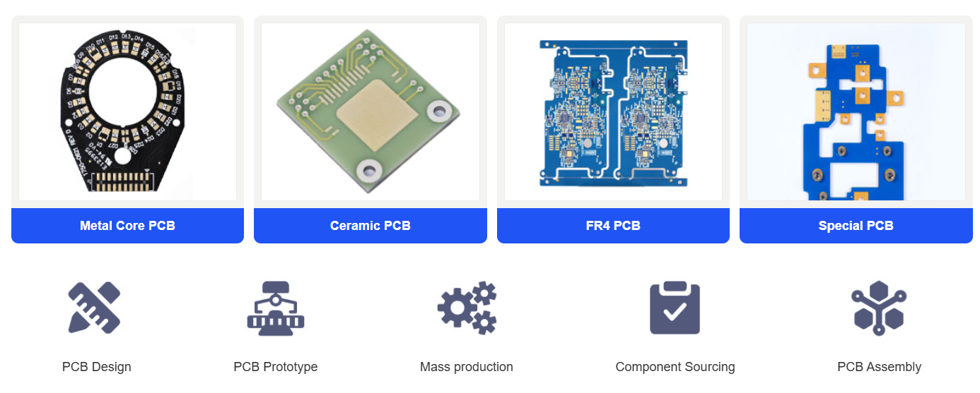
PCB Design & DFM Check – We don’t just manufacture—we help you build better boards. Send us your layout or concept, and our senior engineers will review your files for manufacturability, improving your design before it hits the production line.
PCB Fabrication – Single-layer, multi-layer, HDI, aluminum-based, or ceramic—we fabricate PCBs of all complexities. Our in-house plant supports quick turnarounds and strict quality control for every batch.
PCB Prototype – Need your prototype in 24–72 hours? We’ve got your back. Ideal for engineers in the development phase, we offer fast PCB prototyping with full traceability, fly-probe testing, and surface finish options.
PCB Assembly – Our turnkey PCB assembly service covers everything from component sourcing, SMT/DIP soldering, to functional testing. You send us your BOM and Gerber—we handle the rest.
IC Programming – Pre-programming and testing of integrated circuits to streamline your assembly process.
What PCB Types Does EBest Circuit (Best Technology) Manufactured?
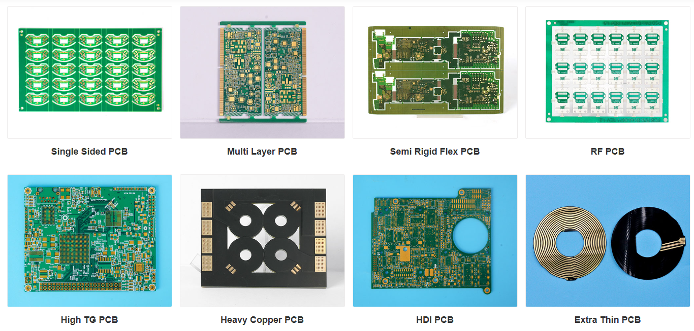
We are capable of manufacturing a wide variety of PCB types, including but not limited to:
FR4 PCBs (high speed PCB, IC substrate, high TG PCB, extra thin PCB, our special semi-rigid flex PCB and so on.)
Metal Core MCPCBs (aluminum based PCB, copper clad PCB, sinkpad PCB, thermoelectric copper separate PCB)
Ceramic PCBs (AlN, BeO, Al₂O₃, Zro2)
Flexible and Rigid-Flex PCBs, FFC, Dual access PCB
HDI PCBs
High-Frequency PCBs
Heavy Copper PCBs
Busbar PCBs
Hybrid Substrate PCBs
Whether you need high-reliability boards for aerospace, thermally conductive boards for LEDs, or RF boards for communication devices, we have the capability to deliver.
PCB Prototype Lead Time
We understand how crucial speed is in product development. Our standard PCB prototypelead time is:
Single-layer & double-layer PCBs: as fast as 24 hours
4-layer PCBs: typically 48–72 hours
6-layer or above: around 3–5 working days, depending on complexity
Below is a detailed prototype lead time sheet at EBest Circuit (Best Technology), the expedited options are available to meet urgent project deadlines.
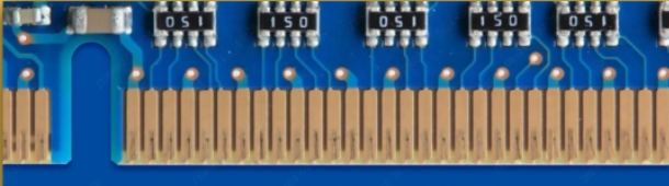
PCB gold finger is a row of gold-plated conductive contact sheets located on the edge of the printed circuit board, named for its shape like a finger and plated with gold. It is usually used to insert the PCB into a connector or card slot for electrical connection and signal transmission. You’ll often find them on expansion cards, memory modules, and interface boards that plug into the motherboard or backplane.
These fingers act as the physical and electrical contact points between the PCB and its slot. They need to be durable, conductive and corrosion-resistant, which is why gold is used. Unlike standard wires or padding, gold fingers must withstand repeated insertion and removal, so wear resistance and high reliability are top priority in their design.
What Material is Gold Fingers Made of?
Gold fingers aren’t pure gold, and they don’t need to be. Instead, they are a multi-layer structure designed for performance, not cost.
At the core is copper, the base layer used in nearly all PCBs. Copper offers excellent electrical conductivity. But copper oxidizes over time, which affects signal transmission. So, a nickel barrier is added next. Nickel prevents the copper from diffusing into the top gold layer and adds hardness.
Finally, a thin layer of gold—either hard electroplated gold or soft immersion gold—is applied on top. Gold is chosen for two key reasons: it’s a great conductor and it doesn’t tarnish or corrode. This ensures long-lasting, high-performance edge connectors.
The amount and type of gold used depend on the application. Some fingers will have a thicker, harder gold layer for high-wear use. Others, used less often, may use thinner or softer gold to save on cost.
Types of PCB Gold Fingers
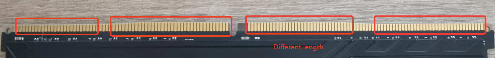
1. Standard PCB Gold Fingers – The most common PCB gold fingers, with horizontal and even arrays. PCB pads have the same length, width and space. This type of gold finger is easy to make.
2. Uneven PCB Gold Fingers – PCB pads have the same width but different lengths and sometimes different spaces like below image showing. For some PCBs, the gold fingers are designed to be shorter than others. The most relevant example of such PCBs is a PCB for a memory card reader, where the device connected to the long finger must first power the device connected to the shorter finger.
3. Segmented PCB Gold Fingers – PCB pads have different lengths, and the gold fingers are segmented. Segmented gold fingers vary in length, and some of them are also disjointed within the same finger of the same PCB. Such PCBs are suitable for waterproof and rugged electronics.
PCB Gold Fingers Manufacture Technical
Not all gold fingers are made using the same process. The method and material used for gold plating affect the performance, durability, and cost of the final product. Let’s take a closer look at the most common types.
Electroless Nickel Immersion Gold (ENIG)
ENIG is a chemical process used to deposit a thin, even layer of gold over a nickel base. It’s not applied using electricity, so it creates a smooth, flat surface. ENIG is known for its excellent surface planarity and is commonly used for surface mount pads. But in gold fingers, it’s less common unless the board will be inserted only a few times. ENIG produces softer gold, which means the plating wears off faster with repeated use.
Electroplated Hard Gold
This is the most popular choice for gold fingers PCB applications. Electroplating uses an electric current to apply a thicker and harder layer of gold, its gold thickness can be up to 50u’’. Hard gold plating usually includes small amounts of cobalt or nickel, which makes the gold layer more rigid. This helps it resist abrasion during multiple insertions into card-edge connectors.
Electroplated hard gold is a bit more expensive than ENIG but lasts longer and offers better performance for edge connectors.
Edge Beveling
Edge beveling isn’t a type of plating but an additional mechanical step. It involves cutting or grinding the PCB edge at an angle, typically 30° or 45°, to make insertion into connectors smoother.
Beveled edges help prevent damage to both the PCB and the mating socket. It also reduces insertion force, minimizing wear and tear. While beveling isn’t mandatory, it’s often recommended when the board will be inserted and removed multiple times.
Gold Fingers vs. Edge Connectors
“Gold fingers” and “edge connectors” are both terms used in PCB design, but they refer to slightly different concepts. Gold fingers are part of the PCB, while edge connectors are part of the device that receives the PCB. Gold fingers are the gold-plated pads at the board’s edge. They’re designed to slide into the slot of an edge connector. The connector itself is usually mounted on a motherboard or backplane, holding the PCB in place and ensuring a stable electrical link.
Feature
Gold Fingers
Edge Connectors
Definition
Gold-plated contact pads on the edge of a PCB
Socket or slot that receives the PCB
Location
Part of the PCB itself
Mounted on a motherboard or host board
Function
Transmit signals and power from PCB to system
Provide physical and electrical connection
Material
Copper + nickel + gold plating
Usually plastic body with internal metal contacts
Durability
Depends on gold thickness and use frequency
Built to withstand repeated insertions/removals
Customization
Length, width, plating, beveling can be customized
Usually standard depending on slot type
Common Use
RAM sticks, GPU boards, industrial control boards
Motherboards, expansion slots, backplanes
Design Consideration
Needs precise layout, spacing, and gold plating
Must match PCB layout and dimensions
Benefits of Designing Gold Fingers at the Edge of PCB
Gold fingers allow boards to be plugged directly into other systems without the need for extra connectors, makes design simpler and install faster.
Gold is highly conductive, so the signals and power of devices enable to pass efficiently through the interface. They are often used in high-frequency or high-speed data applications.
Gold does not oxidize or corrode. Even in moist or harsh environments, it maintains its performance over time.
Hard gold plating can handle thousands of insertions without degrading. That’s why it’s ideal for modular designs or devices that get frequently unplugged.
Gold fingers reduce the need for bulky connectors, allowing for more compact PCB designs—especially valuable in smartphones, wearables, and compact industrial modules.
How Thick Is a PCB Gold Finger?
The gold thickness on fingers typically ranges from 3 to 50u’’, depending on how the PCB will be used. For commercial and industrial use, the standard is usually 30u’’ of hard gold over 100–150u’’ of nickel.
3–10u’’: Suitable for low-cost applications with minimal wear.
15–30u’’: Common for most consumer electronics and industrial devices.
45–50u’’: Used in military or high-end industrial equipment that needs maximum durability.
PCB Gold Finger Plating Process
The hard gold plating process for PCB gold fingers involves several precise and carefully controlled steps. Here’s how it’s done:
1) Apply Blue Protective Mask
All areas of the PCB surface except the gold finger pads are covered with a blue protective mask. This ensures that only the contact pads receive hard gold plating. The conductive areas are aligned consistently with the board’s orientation to maintain plating accuracy.
2) Remove Oxide Layer from Copper Pads
Next, the oxidation layer on the copper surface of the gold finger pads is removed. We use sulfuric acid for this step, followed by a water rinse. Then, the surface is mechanically scrubbed to ensure it’s fully clean. After that, we rinse the surface again using water and deionized water to eliminate any residues.
3) Electroplate Nickel onto Copper Pads
A nickel layer is then electroplated onto the clean copper surface of the gold finger pads. This layer serves as a barrier and bonding surface for the gold. After plating, the surface is thoroughly rinsed again with water and deionized water to remove any remaining nickel solution.
4) Electroplate Hard Gold over Nickel
Now comes the hard gold plating step. A layer of gold is electroplated onto the nickel-coated pads. This provides durability, conductivity, and wear resistance. Any unused gold solution is recovered for reuse. Finally, the plated area is cleaned again—first with water, then with deionized water—to ensure a spotless surface.
5) Remove Blue Mask
With the hard gold plating complete, the blue protective mask is removed. The PCB is then ready to move forward in the manufacturing process, beginning with the solder mask printing step.
Design for Manufacturability (DFM) of PCB Gold Fingers
1. Beveling Design for Gold Fingers
The safe distance between the gold fingers and the PCB outline edge must be considered. This depends on the final board thickness and the bevel angle. Common bevel angles are 45o.
If the gold fingers are too close to the board edge, copper may be exposed during beveling. To avoid this, copper should be trimmed based on specific parameters as below. However, if you do not want to shorten the gold fingers, increase the safety distance between them and the board edge as per the recommended values.
Bevel Angle
Board Thickness (mm)
Remaining Thickness (mm)
Beveling Depth (mm)
20o
1.6
0.5
1.51
3.0
0.65
1.85
2.5
0.7
2.47
30o
1.0
0.5
0.44
1.2
0.5
0.60
1.6
0.5
0.95
2.0
0.65
1.16
2.5
0.7
1.56
45o
1.0
0.5
0.25
1.2
0.5
0.35
1.6
0.5
0.55
2.0
0.65
0.68
2.5
0.7
0.9
2. Solder Mask Opening Design
To ensure easy insertion into connectors, no solder mask should be applied over the gold finger area. Full openings must be designed here. If the area is not fully opened, solder mask ink between gold fingers can peel off after repeated insertion/removal, which may affect contact reliability.
Gold finger and tin finger areas must have solder mask openings that extend approximately 10 mil beyond the board edge.
The solder mask opening should be 4 mil larger than the trace on each side. Make sure that the distance between the opening and surrounding copper is safe to prevent exposed copper. If copper is exposed, it must be removed (etched).
No solder mask opening is allowed for vias within 2 mm of the gold finger area.
3. Copper Pour Design on the Signal Layer
To support smoother insertion, avoid copper pour (flooding) in the gold finger region on the outer layers. If multiple fingers share the same net and copper is poured, they might be joined into a single pad, which affects mechanical separation and may interfere with insertion/removal.
4. Uneven Gold Fingers
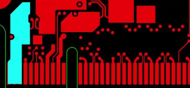
For uneven gold fingers, the main trace should be 40mils, and the auxiliary trace should be 20mils. The connecting point should be 6mils, and the distance between the pad and the 20mil auxiliary trace should be 8mils. After adding the staggered traces, the main trace should be shifted to maintain an 8mil spacing from the long finger pad.
When the main trace enters the board, it should be connected using a diagonal line. If there’s a large groove beside the finger, the trace should be curved, not angled.
How Are PCB Gold Fingers Used?
Gold fingers are found in a wide variety of applications across many industries:
Computers: RAM modules, GPUs, and expansion cards all use gold fingers to connect to the motherboard.
Consumer Electronics: Devices like game consoles, smart TVs, and wearables use gold fingers for modular connections.
Medical Devices: Equipment requiring high reliability often includes gold fingers for secure signal transfer.
Industrial Automation: Boards that plug into PLCs or backplanes use gold fingers to keep connections stable in harsh environments.
Aerospace and Defense: Mission-critical systems rely on hard gold fingers for consistent performance and durability.
FAQs
1. What’s the Ideal Thickness for PCB Gold Fingers?
Most designs use 30μin of hard gold.
2. Are Gold Fingers Always Beveled?
Not always, but beveling helps reduce insertion wear. It’s recommended if the board is plugged in and out often.
3. How Do I Know If I Need ENIG or Hard Gold?
Use ENIG for light-use connectors or where solderability matters. Go for hard gold when durability and frequent insertions are key.
4. How Much Does PCB Gold Fingers Cost?
PCB gold fingers cost depends on gold thickness, finger length, and quantity. Thicker gold and more fingers increase cost, but also improve lifespan. Contact EBest Circuit (Best Technology) to get a quotation.
5. Can Gold Fingers Be Repaired?
Usually, no. Once worn or damaged, the board often needs to be replaced.
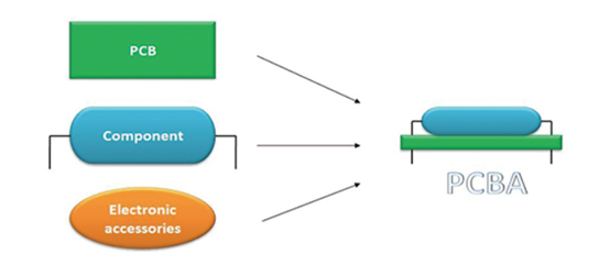
It’s a complete board where all parts are mounted and ready to work. The bare board itself is called a PCB. But once components like resistors, capacitors, and chips are soldered onto it, it becomes a PCBA. Sometimes, some electronic accessories will be soldered onto the PCB surface as well.
Key Components in PCBA
The value of a PCBA comes from the components it carries. Each part plays a role in how the circuit works. Let’s go over some of the most common parts:
Resistors: Control the flow of current.
Capacitors: Store and release energy when needed.
Inductors: Manage signals, especially in filters.
Diodes: Let current flow in one direction only.
Transistors: Switch or amplify signals.
ICs (Integrated Circuits): Small chips with many tiny parts inside. They perform complex functions.
Connectors: Help connect the board with other systems.
Transformers: Change voltage levels for safer or better operation.
All these parts must be carefully chosen and placed. A small mistake can stop the board from working right. That’s why design and assembly matter so much.
Types of PCBA Assembly Techniques
1. Surface Mount Technology (SMT)
This is the most common method today. Components are placed directly on the surface of the board. Pick and place machines handle most of the work, which keeps it fast and accurate. SMT supports miniaturized parts and high-speed production.
2. Through-Hole Technology (THT)
This technique uses components with leads that go through holes in the PCB. These leads are soldered on the other side. THT is strong and used for large or high-stress parts like connectors or transformers.
3. Mixed Technology Assembly
Some boards use both SMT and THT. Surface-mount parts go on first, then through-hole components are added by manually. This mix allows for flexible, compact, and reliable designs.
What is the difference in PCB and PCBA?
Though the terms PCB and PCBA are often used together, they describe very different stages in the electronics manufacturing process. And you must to know: PCB are one of important part of PCBA, but PCBA not. Below we listing the key differences between them:
Factor
PCB
PCBA
Stage
Blank board
Assembled with components
Components
No
YES
Functionality
Non-functional
Fully operational
Manufacturing Cost
Low
Higher (because include the components cost)
Testing
Basic inspection
Complete electrical testing
Assembly Techniques
Not applicable
SMT, THT, or hybrid
Files Needed
Gerber, drill files
Gerber, BOM, pick & place, assembly files
Lead Time (under same design)
Short
Related longer than PCB
What Is the Use of PCBA?
PCBAs are used in almost everything you see around:
Phones: Control your screen, camera, and sound.
Computers: Process data, run programs.
Vehicles: Support GPS, safety features, engine control.
Medical devices: Power equipment like MRI or ECG machines.
Home appliances: From smart TVs to microwave ovens.
Without a PCBA, none of these would work. It’s like the brain of any electronic device. From simple tools to high-end gadgets, PCBA plays a big role.
How to Do PCBA Testing?
Testing makes sure the board works as expected. It helps catch issues before the board goes into the final product. There are several ways to test a PCBA:
1. Visual Inspection
This is the first step. Technicians or machines check if parts are in the right place. They also look for bad solder joints, cracks, or missing items.
2. Automated Optical Inspection (AOI)
AOI mainly uses a camera system scans the board. It checks for incorrect or misaligned parts. It’s faster than manual inspection and works well for large batches.
3. In-Circuit Testing (ICT)
ICT checks each component directly. It makes sure resistors, capacitors, and connections work properly.
4. Functional Testing
This test powers the board and simulates how it will be used. It checks whether the PCBA can perform the expected tasks.
5. X-Ray Inspection
Used when components are hard to see, like BGAs (Ball Grid Arrays). The X-ray looks through the board to catch hidden problems.
6. Flying Probe Test
For small batches, probes test different points without a custom fixture. It’s flexible and cost-effective.
7. Testing with jig
This is used for mass production, jig tools are made according to the design files, so it is a customized. Jig testing can save much time compared with flying probe.
EBest Circuit (Best Technology) deeply know the importance of the product quality, so we pay more attention to the PCB board quality checking process. We set a QC department according to ISO9001:2015 and ensure all processes are compliance with quality system.
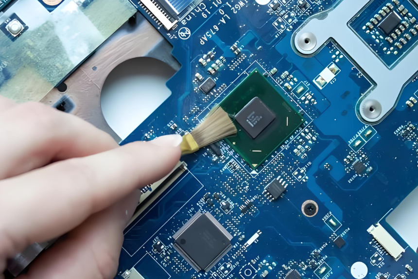
How Do You Clean a PCBA?
During the PCB assembly process, cleaning a PCBA is an important step, especially after soldering. Residual flux, dust, or moisture can affect the performance of the board. Nowadays, the common cleaning methods used in EBest Circuit (Best Technology) are:
1. Manual Cleaning
This is the most basic method. A technician uses a soft anti-static brush and high-purity isopropyl alcohol to remove visible flux or dirt. It’s ideal for prototypes, small batches, or after rework or repair. Manual cleaning gives the operator control, especially in tight or delicate areas. However, it’s time-consuming and not suitable for large-scale production.
2. Ultrasonic Cleaning
Ultrasonic cleaning is widely used for complex boards and mass production. The PCBA is submerged in a tank filled with a cleaning solution. High-frequency sound waves pass through the liquid, creating microscopic bubbles. These bubbles collapse rapidly, producing a scrubbing action known as cavitation.
This technique reaches tiny gaps under components where brushes can’t go. It’s very effective for removing dried flux, fine dust, or ionic contamination. The process is gentle on components but powerful enough to clean even the most compact assemblies. After cleaning, the board is rinsed and dried with warm air or placed in a drying chamber.
3. Dry Ice Cleaning
Dry ice cleaning is a newer, eco-friendly technique. It uses solid CO₂ pellets, also called dry ice, blasted at high speed onto the PCBA surface. As the pellets hit, they turn into gas instantly. This process lifts off dirt, flux, and even adhesives without leaving moisture or residue behind.
Dry ice cleaning works well for delicate electronics and is especially useful in industries where cleanliness must meet strict standards. To give customer a highest quality of the PCBA, our SMT factory equipped with the dry ice cleaning machine to ensure a clear surface while improve the efficiency.
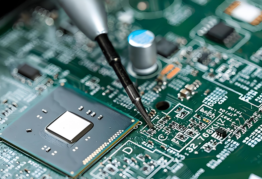
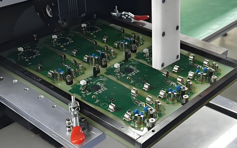
PCBA Assembly Process
The PCBA assembly process is relatively simple than PCB manufacturing, actually the most tedious step is to load all the components on the pick and place machine, and set the program parameters. Here we break down all the processes of the mass production PCB assembly, from the solder paste printing to function testing.
1. Solder Paste Printing
First, solder paste is applied to the bare PCB. This paste is mainly consists of silver and tin, a mix of tiny solder particles and flux. A stencil is placed over the board, and the paste is spread across it using a squeegee. The paste sticks only to the exposed pads where components will be mounted.
2. Load components feeder
Load all the components in the feeder of the pick and place machines, make sure all the parameter of components are correct, and double check the direction of chips. It is a simple but tedious step and need much time to check everything is okay.
2. Pick and Place
After applying solder paste, automated pick-and-place machines begin placing surface-mount components onto the board. These machines work fast and accurately. They follow a file created during PCB design that tells them the exact location for each part. The components sit on the solder paste, which holds them in place temporarily.
3. Reflow Soldering
Next, the assembled board goes through a reflow oven. The oven slowly heats the board in stages. When it reaches a high enough temperature, the solder paste melts and forms strong electrical and mechanical connections between the parts and the board. After this, the board cools down, and the solder solidifies.
This step is only for SMT components. If the board has only through-hole parts, this step may be skipped.
4. Inspection (AOI and Visual)
Once the soldering is done, the board goes through inspection. Automatic Optical Inspection (AOI) machines scan the board using high-resolution cameras. They check for misaligned parts, soldering problems, or missing components. For small production or sensitive areas, manual inspection is also performed to catch anything machines might miss.
5. Through-Hole Component Insertion (If Needed)
If the board uses through-hole technology (THT), this is when those parts are added. Workers or machines insert the components into the holes, and the leads go through to the other side of the board. These components are often bulkier, like connectors or transformers.
6. Wave Soldering (For THT)
For boards with many through-hole parts, wave soldering is used. The board passes over a wave of molten solder that touches the underside. This solders all the leads at once. It’s fast and effective, especially for high-volume production. For small-scale or sensitive boards, hand soldering might be used instead.
7. Final Inspection and Quality Control
After soldering, the entire board is checked again. Technicians or AOI machines inspect the final assembly. They look for cold joints, excess solder, or misplaced parts. Boards may also be tested with X-ray machines to inspect solder joints under BGAs or hidden areas.
8. Functional Testing (FCT)
The next step is functional testing. The board is powered up and tested to make sure it works correctly. This could include checking voltages, signals, response times, and communication with other devices. Engineers may use test jigs or test programs based on the end application.
9. Cleaning (If Needed)
After all soldering and testing, the board might be cleaned to remove flux residue. Depending on the flux used, this could be manual, ultrasonic, or dry ice cleaning. Clean boards are especially important in high-reliability fields like aerospace, automotive, or medical.
10. Conformal Coating or Protection (Optional)
For some applications, a conformal coating is applied. This is a protective layer that shields the board from moisture, dust, and chemicals. It’s often used in harsh environments. Coating can be applied by spraying, dipping, or brushing.
11. Packaging and Shipping
Finally, once the PCBA passes all checks, it’s packed carefully. Anti-static bags, foam, and trays protect it during transport. Labels are added for tracking and traceability. From here, it’s ready to be installed into the final product. Here is a whole process of pcb assembly in EBest Circuit (Best Technology).
PCBA HS Code
Every product for trade needs a code. The HS code for PCBA usually is 8517799000
But depending on the use or market, some customs may use a different classification. For example:
853400 for bare board parts, sometimes be used on certain assembled parts.
847330 for boards used in computers.
853710 for board which used as controller or controller unit.
Noted: Always check with your country’s customs for the right code. Using the wrong one may cause delays or extra costs.
Our PCBA Services
At EBest Circuit (Best Technology), we specialize in end-to-end PCBA services. From design to delivery, we support your project with speed, quality, and reliability. We can be your first choice because:
We have 18+ years in PCB industry
One-Stop Service: PCB fabrication, parts sourcing, SMT/THT assembly, testing
Custom Solutions: From prototypes to mass production, no MOQ
Skilled Engineers: For DFM & DFA checks and process optimization
Strict Quality Control: 9-times QC check, including AOI, X-ray, ICT, and functional testing
Global Delivery: Fast and on time, wherever you are
Component Sourcing: Only original, trusted parts, we have cooperated with digikey, findchips, mouser for over 10 years, and we can get the most competitive price from them.
PCB Fabrication: Rigid, flex, metal-core, ceramic, and more.
A battery eliminator circuit can be short for BEC, it is a circuit that replaces batteries to provide power. Battery eliminator circuits were originally used in applications where the mains was converted to battery power. They are now used in battery-driven applications where high and low power are required, and can be used to save battery demand. For example, when the motor requires 12V and the control board requires 5V, a 12V to 5V battery eliminator circuit is required, and only one set of 12V batteries is required.
Early commercial battery eliminators were produced by Edward Rogers in 1925 as a supplement to his line of “battery-free” radio receivers. Another early battery eliminator manufacturer was Galvin Manufacturing Company (later known as Motorola), which was founded on September 25, 1928 by Paul Galvin and his brother Joseph E. Galvin to build battery eliminators for radio receivers installed in cars.
BECs are also used in some motorcycles and all-terrain vehicles to reduce the use of batteries in order to reduce the weight of the load. The part that originally required the battery is replaced by a large-capacity capacitor, which can be used to reduce the pulse fluctuations produced by the alternator.
Why Is a Battery Eliminator Circuit Important?
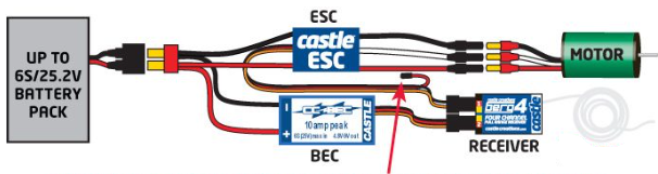
Many electronic circuits require different voltage levels to function correctly. For example, in an RC aircraft or drone, the motor runs on a high-voltage battery pack, but the flight controller, servos, and receiver need a much lower voltage (usually 5V or 6V). Without a BEC, a separate battery would be required for the receiver and servos, adding extra weight and complexity. A BEC solves this issue by stepping down the voltage and supplying consistent power to these essential components.
In addition to this, intercell static electricity is a common phenomenon in electronics, which can produce a transient high voltage in electronic devices, resulting in damage to batteries and devices. And the static electricity between batteries may cause problems such as short circuit, leakage, and overheating of batteries, or even fire and explosion. The battery eliminator circuit connects the electrostatic charge between the battery and the ground through the grounding principle, so that the charge is lost, so as to protect the safety of the battery and equipment.
Types of Battery Eliminator Circuits
There are two main types of BECs in the electronics, each with distinct advantages and applications:
1. Linear BEC
A linear battery eliminator circuit uses a linear voltage regulator to reduce voltage. It is commonly used in remote-controlled (RC) models, especially as part of an electronic speed controller (ESC). This circuit allows the RC model to operate with a single battery pack that powers both the motor and control electronics, eliminating the need for a separate battery for the receiver and servos.
A BEC within the linear regulator often includes a low-voltage cutoff function to prevent excessive battery discharge, which could lead to system failure. It is typically installed according to the manufacturer’s recommendations, and the regulated voltage is optimized for the RC receiver.
2. Series BEC (SBEC)
A series battery eliminator circuit is a design that uses a basic series switching regulator to provide a stable DC voltage output. It is commonly used in 9V DC applications, with a maximum current not exceeding 100mA. This circuit includes components such as a transformer, filter capacitor, and push-pull rectifier, which help step down the voltage and provide isolation protection.
When unloaded, the circuit outputs approximately 18V DC, and under full load, the voltage drops to around 12V DC. Additionally, it features an output buffer amplifier, which enhances current gain and voltage regulation.
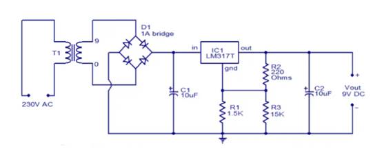
Battery Eliminator Circuit Diagram
A BEC battery eliminator circuit consists of several key components that regulate voltage and maintain stability. A basic battery eliminator circuit diagram includes:
Voltage Regulator – The core component that steps down voltage.
Capacitors – Stabilize the output voltage and filter noise.
Diodes – Provide reverse polarity protection to prevent damage.
Input and Output Terminals – Allow connection to a power source and the electronics that need power.
Below is a series circuit diagram of the battery eliminator circuit, which can be used as a replacement for the 9VPP3 battery. The circuit given here can be used to power any device powered by a 9V battery. Transformer T1 reduces the supply voltage and bridge D1 performs rectification. Capacitor C1 is a filter. The ICLM317T is a voltage regulator. If the values of R1, R2, and R3 are selected, the output voltage of IC1 will be stable at 9 volts.
What Does a Battery Eliminator Circuit Do?
A battery eliminator circuit provides a stable and regulated power supply to electronic components that would otherwise require a separate battery. It ensures that these components receive the correct voltage level, preventing damage due to overvoltage or undervoltage. The mainly functions of a BEC including:
Voltage Regulation – Converts high voltage from the main power source into a stable lower voltage for sensitive electronics.
Weight Reduction – Eliminates the need for extra batteries, making devices lighter and more efficient.
Power Management – Protects components from voltage fluctuations and power surges.
Improved Efficiency – Reduces power wastage and enhances performance in drones, RC models, and embedded systems.
For example, in an RC car, the motor may run on a 7.4V or 11.1V battery pack, but the receiver and servos require only 5V or 6V.
How Does a Battery Eliminator Circuit Work?
A battery eliminator circuit works by taking power from a high-voltage source, regulating it, and supplying a stable output voltage. The working principle varies based on whether it is a linear BEC or a switching BEC.
A linear BEC operates like a traditional voltage regulator, reducing voltage by converting excess energy into heat. For instance, if a 12V input is required to provide 5V output, the extra 7V is dissipated as heat. This method is simple but inefficient for high-power applications since it generates excess heat.
While different with linear BEC, a series BEC (also known as SBEC or UBEC) uses a high-frequency switching regulator to convert voltage without significant heat loss. Instead of dissipating excess voltage, it switches the power on and off rapidly, storing and releasing energy efficiently.
Battery Eliminator Circuit Uses
A BEC is used in various applications where a stable power source is needed. Some of the most common uses include:
RC Vehicles and Drones – Powers receivers, servos, and electronic speed controllers (ESCs).
FPV Systems – Supplies steady voltage for cameras, video transmitters, and OSD modules.
Embedded Systems – Provides regulated power to microcontrollers, sensors, and digital circuits.
Power Tools – Eliminates the need for disposable batteries in low-voltage applications.
Testing and Prototyping – Used in laboratories and research to power circuits with precise voltage levels.
What Is the Difference Between BEC and UBEC?
A BEC and UBEC (Universal Battery Eliminator Circuit) serve the same function but differ in design and efficiency.
Feature
BEC
UBEC
Type
Can be linear or switching
Always a switching regulator
Efficiency
Lower for linear BECs
Higher efficiency
Heat Generation
Higher in linear BECs
Minimal due to switching technology
Current Handling
Limited
Can handle higher currents
Ideal Use
Low-power applications
High-power RC and drone systems
A UBEC is a more advanced version of a BEC, commonly used in RC drones, FPV systems, and high-current applications where power efficiency is crucial.
BEC in FPV Drone Flight Controllers
In FPV (First-Person View) drones, a battery eliminator circuit drone is used to maintain stable voltage levels across different electronic components. Flight controllers, video transmitters, and cameras all require a reliable power source to function properly. Without a BEC, these components would need separate batteries, adding unnecessary weight and complexity to the drone.
Drones typically use high-voltage LiPo (Lithium Polymer) batteries, often rated at 3S (11.1V), 4S (14.8V), or even higher. However, many essential components operate at lower voltages, such as 5V or 9V. A BEC steps down the voltage from the main battery and ensures that all connected components receive the correct power level. By integrating BEC into a FPV drone, it functions:
Stable Flight Controller Operation
The flight controller (FC) is the central processing unit of the drone, managing stabilization, motor control, and sensor inputs. A BEC prevents voltage fluctuations, ensuring smooth operation and reducing the risk of crashes due to power instability.
Reliable Power for FPV Cameras
FPV cameras require a steady voltage to avoid video signal noise or sudden blackouts. A BEC eliminates power spikes, which could interfere with video transmission and affect flight visibility.
Consistent Power to Video Transmitters (VTX)
The video transmitter (VTX) sends live footage from the drone to the FPV goggles or monitor. Inconsistent power can cause signal drops, static, or overheating. A BEC delivers a clean, regulated voltage, improving video signal stability.
Prevents Overheating and Component Damage
Directly connecting a high-voltage battery to low-voltage components can cause overheating and failure. A BEC protects these parts, extending their lifespan and reducing the chance of mid-flight failures.
Many modern flight controllers include an integrated BEC, simplifying power distribution. However, for higher power demands, external switching BECs (UBECs) provide better efficiency and handle larger current loads without overheating.
At EBest Circuit (Best Technology), we provide drone printed circuit boards with battery eliminator circuits. We have passed AS9100D certifications, and set a specialized QA system according to AS9100D, build up procedure to aim specifically at the prevention of problems and the elimination of root causes, provides complete traceability of material and detailed processing history for all products manufactured. If you are interested in the manufacturing of drone PCB with BECs, you are welcome to touch us for more details.
A solder mask also called solder resist, it is a protective layer applied to a printed circuit board (PCB) to shield copper traces from oxidation, contamination, and unintended solder bridges. Without this layer, exposed copper can easily corrode or cause short circuits due to accidental solder connections.
Most solder masks are made from epoxy resins, liquid photo imageable (LPI) materials, or dry films. These materials create an insulating layer that only exposes the necessary contact points for soldering, such as component pads. In modern PCB manufacturing, solder masks are essential for ensuring proper functionality, ease of assembly, and long-term reliability. Whether for simple or advanced circuits, a high-quality solder mask is critical for maintaining the integrity of a PCB.
How Is Solder Mask Applied to Your PCB?
How is solder mask applied to your PCB? Applying a solder mask is a multi-step process that requires precision to ensure even coverage and proper functionality. The process varies depending on the type of solder mask used, but the general steps include:
1. Surface Preparation
Before applying a solder mask, the PCB surface must be thoroughly cleaned. Any dust, grease, or oxidation can affect adhesion. Manufacturers use chemical cleaning or mechanical scrubbing to remove contaminants and prepare the board for coating.
2. Solder Mask Application
The solder mask is applied using one of the following methods:
LPI Solder Mask: A liquid mask is sprayed or screen-printed onto the PCB surface. This method provides excellent precision and is widely used in high-density PCB designs.
Dry Film Solder Mask: A pre-cured solder mask film is laminated onto the board and then exposed to UV light for patterning. It is a common method in high-volume manufacturing.
Epoxy-Based Solder Mask: A thermosetting polymer is screen-printed onto the board and then cured. This is one of the oldest methods but is less precise than LPI.
3. UV Exposure and Developing
After application, the board is exposed to ultraviolet (UV) light through a photomask that defines the solder mask openings. The exposed areas harden, while the unexposed parts remain soft and can be removed using a developer solution.
4. Curing and Final Inspection
Once the mask is developed, the PCB undergoes a curing process, usually in an oven, to fully harden the solder mask. Afterward, the board is inspected to ensure the mask is properly applied without defects. Evenly application of the solder mask is essential for preventing soldering issues and ensuring the long-term reliability of the PCB.
Why Is the Solder Mask Green?
The green color of solder masks became the industry standard due to a combination of historical, practical, and technical factors. Early PCB manufacturing processes used epoxy-based resins, which naturally had a green tint. Over time, manufacturers standardized this color because it offered excellent contrast for visual inspection. Engineers and technicians rely on automated optical inspection (AOI) systems to detect defects, and the green color provides the best balance between visibility and eye strain. Other colors like red, blue, and black exist, but green remains the most widely used due to its well-established reliability and cost-effectiveness.
Beyond visibility, green solder masks also offer superior thermal and chemical stability compared to some other colors. PCBs endure high temperatures during soldering, and green formulations have been extensively tested to withstand heat without degrading.
What Can I Use Instead of a Solder Mask Material?
If a solder mask isn’t available, there are alternative methods to protect PCB copper traces. However, they may not provide the same level of durability and precision.
1. Conformal Coatings
Conformal coatings are thin protective layers applied to PCBs to protect against moisture, dust, and corrosion. While they don’t replace solder masks, they can provide an extra layer of protection. Some PCBAs may required to coating a layer of conformal as an extra protect layer.
2. Kapton Tape
Kapton tape is a heat-resistant, electrically insulating material that can be used to protect specific areas of a PCB. However, it doesn’t offer the same level of coverage or durability as a solder mask.
3. PCB Lacquers
Some manufacturers use specialized PCB lacquers to coat copper traces and prevent oxidation. These coatings are easy to apply but may wear off over time.
4. DIY Solutions
Some electronics hobbyists use clear nail polish as a temporary solder mask substitute. While it can offer short-term protection, it is not a recommended solution for professional PCBs.
A proper solder mask is always the best choice for ensuring the longevity and reliability of a PCB.
How Do You Apply Solder Mask Evenly?
A smooth and uniform solder mask application is crucial for avoiding defects. Here are some key factors to consider:
1. Clean the PCB Surface: Any dust or grease can cause uneven adhesion. Proper cleaning ensures the mask spreads evenly.
2. Use Controlled Application Methods: Automated spraying, screen printing, or laminating techniques help distribute the solder mask uniformly.
3. Maintain Proper Viscosity: If the solder mask is too thick or too thin, it may not spread evenly. Maintaining the right consistency ensures better coverage.
4. Ensure Proper Curing: Over-curing or under-curing can create issues with adhesion and durability. Controlled UV exposure and thermal curing help achieve the best results.
What Is the Solder Mask Requirement?
Solder mask requirements vary depending on PCB design, industry standards, and application needs. The mask must very good to protect the board from oxidation, solder bridges, and contaminants. Manufacturers should follow strict guidelines to ensure the solder mask meets performance and quality expectations. And customers also can inspect these parameters to make sure solder mask is good.
1. Thickness Requirements
The solder mask must maintain a consistent thickness to prevent defects. Typical thickness values are:
Over Copper Traces: 15–35 μm (micrometers)
Over Substrate (Bare Board Areas): 5–15 μm
Near SMD Pads and Through-Holes: Sufficient clearance to avoid interference with soldering.
An uneven or excessively thick mask can cause soldering issues, while a thin mask may not provide enough protection.
2. Registration Accuracy
The solder mask must align precisely with the PCB layout. Misalignment can lead to:
Blocked SMD pads or vias, affecting solderability.
Unprotected traces, increasing the risk of oxidation or short circuits.
Industry standards, such as IPC-6012, define the allowable misregistration, typically within ±3 mils (±0.075 mm) to ensure proper coverage.
3. Clearance and Openings
The solder mask must be designed with appropriate clearances around pads and vias to ensure smooth soldering. Key points include:
Pad-to-solder mask clearance: Typically 3–5 mils (0.075–0.125 mm) to prevent solder mask from covering pad edges.
Via coverage: Some designs require tenting (fully covering the via), while others leave vias exposed for better connectivity.
4. Electrical Insulation Properties
Solder masks act as an insulating layer to prevent short circuits between copper traces. The dielectric strength must be high enough to withstand PCB operating voltages. Common requirements include:
Dielectric strength: Above 500V/mil for proper insulation.
Surface resistivity: Greater than 10⁹ Ω/sq to prevent leakage currents.
5. Compliance with Industry Standards
Solder mask materials and application processes must comply with international standards, such as: IPC-SM-840, RoHS & REACH, UL 94V-0.
What Kinds of Solder Masks Do We Have in EBest Circuit (Best Technology)?
At EBest Circuit (Best Technology), we offer a range of solder masks to suit different PCB applications. Our selection includes:
Green (commonly select)
Red (for prototype)
Blue (for power supply board)
Black (consumer electronics)
Matte Black (high-end products or prototypes)
White (lightings)
Grey (prototypes)
Matte Grey (prototypes)
Yellow (rarely used)
Purple (prototype or high-end product that need good appearance)
We ensure that our solder masks meet industry standards, providing excellent adhesion, thermal stability, and long-term reliability. Would you like to discuss a specific solder mask for your PCB project? Contact us today!
DC and AC inverters are essential components in today’s energy systems. Whether you’re harnessing the power of the sun with solar panels, working with backup power solutions, or simply need a way to power your devices, understanding how these inverters work is crucial. This blog breaks down the purpose, advantages, and practical use of DC and AC inverters, helping you make informed decisions based on your needs.
What is a DC and AC Inverter?
Inverters are electrical devices that convert DC (direct current) to AC (alternating current), or vice versa. Typically, DC power comes from sources like batteries or solar panels, while AC is what you use to power most household appliances. A DC to AC inverter is used to convert the DC power into usable AC power. On the other hand, an AC to DC inverter does the reverse, converting AC power into DC to charge batteries or power DC devices.
In simple terms, a DC to AC inverter allows you to use power from sources like batteries or solar panels in everyday devices that require AC power, such as fans, lights, and even refrigerators. Without inverters, it would be challenging to use energy from renewable sources for traditional home appliances.
What is the Purpose of a DC to AC Inverter?
The primary purpose of a DC to AC inverter is to make DC power usable for AC appliances. Whether you’re working with a solar power system or simply need backup power, inverters are the key to making this energy conversion happen. For example, if you’re using a solar panel setup, you typically generate DC power. Since most home appliances run on AC, you need an inverter to convert that energy into a form you can use.
Inverters are essential in off-grid applications, such as in remote areas, where the electricity grid is unavailable. They provide an efficient way to use stored DC power, converting it into AC electricity for devices that would otherwise be useless.
How Does an Inverter Work When There is No Electricity?
When there’s no grid electricity, inverters can still work by drawing power from other sources like batteries or solar panels. This is particularly helpful in off-grid or emergency situations. The inverter takes the DC power from your stored energy and converts it into AC power to keep your appliances running.
For example, if you have a solar power system with a battery backup, and the power goes out, the inverter allows you to keep your appliances on, as long as your batteries have enough charge. In this way, inverters provide an essential role in maintaining power continuity during outages.
DC Inverter AC Advantages and Disadvantages
DC inverters come with several benefits, particularly in renewable energy applications like solar power systems. They are highly energy-efficient and help convert power from DC sources into usable AC power without much loss. This makes them perfect for off-grid living or areas where solar panels are the primary source of energy.
However, there are some drawbacks. DC inverters may have higher upfront costs, and the complexity of conversion can lead to minor energy losses. They also tend to require more maintenance due to the way they manage energy conversion.
On the flip side, AC inverters are generally more efficient in household and industrial settings because AC power is more compatible with most appliances. Their downside lies in the additional energy needed to convert AC power into usable DC energy when dealing with solar systems or battery charging applications.
Despite these differences, both types of inverters have their place, and their advantages often outweigh the disadvantages when used in the right scenarios.
Which is Better: AC Inverter or DC Inverter?
Choosing between an AC and DC inverter depends on your specific needs. AC inverters are more commonly used for residential and industrial applications, as they are designed to power traditional household appliances. They are easy to integrate into existing power systems and typically provide a reliable power source for most needs.
On the other hand, DC inverters are especially useful for renewable energy applications. If you’re installing solar panels or using a battery backup, a DC inverter is the best choice, as it can convert the stored DC power into AC power for your home. They are also more energy-efficient in off-grid situations, where you rely entirely on solar or battery power.
Ultimately, the “better” inverter is the one that fits your particular power needs. If you’re on the grid or need to power AC devices from a DC source, an AC inverter is the way to go. But for renewable energy setups, DC inverters are a better fit.
How Long Will a 12V Battery Last with an Inverter?
The lifespan of a 12V battery when used with an inverter largely depends on the wattage of the devices you’re powering. Inverters typically drain the battery at different rates based on the energy demand of the connected devices. For instance, if you’re running a light or small appliance, the battery can last for several hours. However, larger appliances like refrigerators or air conditioners will drain the battery much faster.
On average, a 12V battery can provide power for anywhere from 3 to 10 hours with an inverter, depending on the load. It’s essential to size your inverter and battery capacity properly to ensure your system works efficiently. By balancing energy use with battery life, you can maximize the performance of your inverter system.
How to Choose a DC AC Inverter?
Choosing the right DC to AC inverter involves considering several factors. First, determine the type of devices you’ll be powering. Consider the total wattage your devices require. Inverters come in various sizes and capacities, so it’s essential to match the inverter’s output with your needs.
Next, consider the efficiency of the inverter. More efficient models will waste less power and give you better performance, especially if you’re using renewable energy sources like solar power. You should also think about the inverter’s durability, features like surge protection, and whether it has any warranties or support.
The inverter’s voltage rating must also align with your power system. For example, in a 12V system, you should choose a 12V DC to AC inverter. Also, remember to check the inverter’s surge capacity, especially if you’re powering devices with a high initial startup load, like motors.
Why PCB is Important in DC and AC Inverters?
PCBs (Printed Circuit Boards) play a crucial role in both DC and AC inverters by providing the necessary connections and support for various electrical components. Inverters rely on PCBs to ensure proper functionality, reliability, and safety. For DC to AC conversion, the PCB helps in routing the signals between critical components like transistors, diodes, and capacitors, ensuring the conversion process runs smoothly.
In both types of inverters, the PCB also helps dissipate heat, manage power efficiently, and prevent potential short circuits. High-quality PCBs are essential for maintaining the long-term durability and performance of inverters, particularly in energy-intensive applications like solar or backup power systems. The design, material quality, and structure of the PCB can directly affect the efficiency and lifespan of the inverter, making it a key component in any inverter system.
With over 18 years of experience in the PCB manufacturing industry, EBest Circuit (Best Technology) is a trusted name in providing high-quality, reliable PCBs for various applications, including inverters. Our expertise and commitment to innovation allow us to create tailored solutions for both residential and industrial energy systems. Whether you’re looking for robust PCBs for solar inverters, backup power solutions, or any other inverter application, EBest Circuit (Best Technology) ensures precision and durability in every product we deliver. For more information about PCB and PCB assembly, pls feel free to contact us at sales@bestpcbs.com.
FAQs
1. What is the main difference between a DC inverter and an AC inverter?
The main difference is that a DC inverter converts direct current (DC) to alternating current (AC), while an AC inverter converts AC to DC.
2. Can an inverter work without a power source?
Yes, inverters can still function when connected to a backup power source, such as a battery or solar panel, even if there’s no grid electricity.
3. How do you size an inverter for your needs?
The inverter should be sized based on the wattage of the devices you want to power. Make sure the inverter’s output matches or exceeds the required load.
4.What are the typical applications of a DC to AC inverter?
DC to AC inverters are typically used in off-grid applications, renewable energy systems, and backup power solutions.
5. Do DC inverters have better energy efficiency than AC inverters?
Yes, DC inverters are generally more energy-efficient in solar and battery-based systems as they convert stored energy directly without much loss.